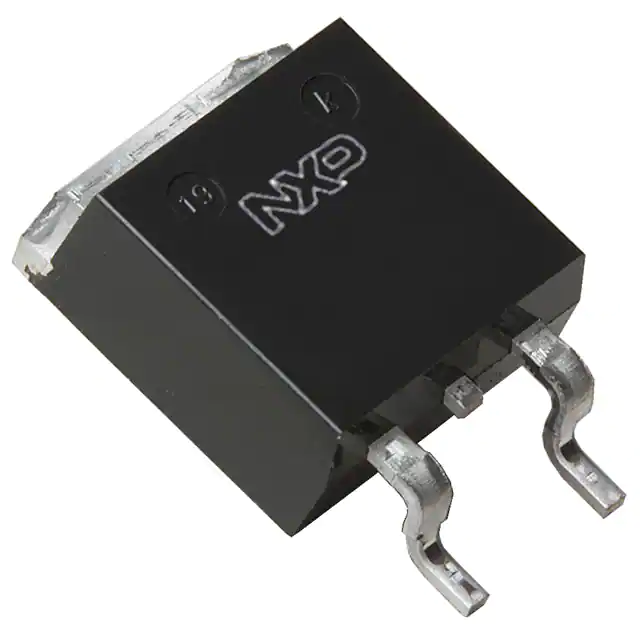
BUK7608-40B
N-channel TrenchMOS standard level FET
Rev. 04 — 24 September 2008
Product data sheet
1. Product profile
1.1 General description
Standard level N-channel enhancement mode Field-Effect Transistor (FET) in a plastic
package using TrenchMOS technology. This product has been designed and qualified to
the appropriate AEC standard for use in automotive critical applications.
1.2 Features and benefits
Low conduction losses due to low
on-state resistance
Suitable for standard level gate drive
sources
Q101 compliant
Suitable for thermally demanding
environments due to 175 °C rating
1.3 Applications
12 V loads
General purpose power switching
Automotive systems
Motors, lamps and solenoids
1.4 Quick reference data
Table 1.
Quick reference
Symbol Parameter
Conditions
Min
Typ
Max
Unit
-
-
40
V
-
-
75
A
VDS
drain-source voltage Tj ≥ 25 °C; Tj ≤ 175 °C
ID
drain current
VGS = 10 V; Tmb = 25 °C;
see Figure 1; see Figure 3;
Ptot
total power
dissipation
Tmb = 25 °C; see Figure 2
-
-
157
W
ID = 75 A; Vsup ≤ 40 V;
RGS = 50 Ω; VGS = 10 V;
Tj(init) = 25 °C; unclamped
-
-
241
mJ
VGS = 10 V; ID = 25 A;
VDS = 32 V; Tj = 25 °C; see
Figure 14
-
12
-
nC
VGS = 10 V; ID = 25 A;
Tj = 25 °C; see Figure 12;
see Figure 11
-
6.6
8
mΩ
[1]
Avalanche ruggedness
EDS(AL)S non-repetitive
drain-source
avalanche energy
Dynamic characteristics
QGD
gate-drain charge
Static characteristics
RDSon
[1]
drain-source
on-state resistance
Continuous current is limited by package.
�BUK7608-40B
Nexperia
N-channel TrenchMOS standard level FET
2. Pinning information
Table 2.
Pinning information
Pin
Symbol
Description
Simplified outline
1
G
gate
2
D
drain
3
S
source
mb
D
mounting base; connected to
drain
Graphic symbol
mb
[1]
D
G
mbb076
S
2
1
3
SOT404
(D2PAK)
[1]
It is not possible to make a connection to pin 2.
3. Ordering information
Table 3.
Ordering information
Type number
Package
Name
Description
BUK7608-40B
D2PAK
Plastic single-ended surface-mounted package (D2PAK); 3 leads (one
lead cropped)
Version
SOT404
4. Limiting values
Table 4.
Limiting values
In accordance with the Absolute Maximum Rating System (IEC 60134).
Symbol
Parameter
Conditions
Min
Max
Unit
VDS
drain-source voltage
Tj ≥ 25 °C; Tj ≤ 175 °C
-
40
V
VDGR
drain-gate voltage
RGS = 20 kΩ
-
40
V
VGS
gate-source voltage
-20
20
V
ID
drain current
Tmb = 25 °C; VGS = 10 V; see Figure 1; see Figure
3;
[1]
-
101
A
Tmb = 100 °C; VGS = 10 V; see Figure 1;
[1]
-
71
A
Tmb = 25 °C; VGS = 10 V; see Figure 1; see Figure
3;
[2]
-
75
A
IDM
peak drain current
Tmb = 25 °C; tp ≤ 10 µs; pulsed; see Figure 3
-
407
A
Ptot
total power dissipation
Tmb = 25 °C; see Figure 2
-
157
W
Tstg
storage temperature
-55
175
°C
Tj
junction temperature
-55
175
°C
Source-drain diode
IS
ISM
source current
peak source current
Tmb = 25 °C;
[1]
-
101
A
Tmb = 25 °C;
[2]
-
75
A
-
407
A
tp ≤ 10 µs; pulsed; Tmb = 25 °C
©
BUK7608-40B_4
Product data sheet
Rev. 04 — 24 September 2008
Nexperia B.V. 2017. All rights reserved
2 of 12
�BUK7608-40B
Nexperia
N-channel TrenchMOS standard level FET
Table 4.
Limiting values …continued
In accordance with the Absolute Maximum Rating System (IEC 60134).
Symbol
Parameter
Conditions
Min
Max
Unit
-
241
mJ
Avalanche ruggedness
non-repetitive
ID = 75 A; Vsup ≤ 40 V; RGS = 50 Ω; VGS = 10 V;
drain-source avalanche Tj(init) = 25 °C; unclamped
energy
EDS(AL)S
[1]
Current is limited by power dissipation chip rating.
[2]
Continuous current is limited by package.
003aac081
120
003aac070
120
Pder
(%)
ID
(A)
80
80
(1)
40
40
0
0
0
50
100
150
0
200
50
100
150
Fig 1.
Continuous drain current as a function of
mounting base temperature
200
Tmb (°C)
Tmb (°C)
Fig 2.
Normalized total power dissipation as a
function of solder point temperature
003aac079
103
Limit RDSon = VDS / ID
ID
(A)
tp = 10 μs
102
100 μs
(1)
1 ms
10
10 ms
100 ms
DC
1
10−1
1
102
10
VDS (V)
Fig 3.
Safe operating area; continuous and peak drain currents as a function of drain-s
©
BUK7608-40B_4
Product data sheet
Rev. 04 — 24 September 2008
Nexperia B.V. 2017. All rights reserved
3 of 12
�BUK7608-40B
Nexperia
N-channel TrenchMOS standard level FET
5. Thermal characteristics
Table 5.
Thermal characteristics
Symbol
Parameter
Rth(j-a)
Rth(j-mb)
Conditions
Min
Typ
Max
Unit
thermal resistance from mounted on a printed-circuit board;
junction to ambient
minimum footprint
-
50
-
K/W
thermal resistance from see Figure 4
junction to mounting
base
-
-
0.95
K/W
003aac080
1
Zth(j − mb)
(K / W)
δ = 0.5
0.2
10−1
0.1
0.05
0.02
10−2
single pulse
δ=
P
t
tp
10−3
10−6
tp
T
T
10−5
10−4
10−3
10−2
10−1
1
tp (s)
Fig 4.
Transient thermal impedance from junction to mounting base as a function of pulse duration
©
BUK7608-40B_4
Product data sheet
Rev. 04 — 24 September 2008
Nexperia B.V. 2017. All rights reserved
4 of 12
�BUK7608-40B
Nexperia
N-channel TrenchMOS standard level FET
6. Characteristics
Table 6.
Symbol
Characteristics
Parameter
Conditions
Min
Typ
Max
Unit
drain-source
breakdown voltage
ID = 0.25 mA; VGS = 0 V; Tj = 25 °C
40
-
-
V
ID = 0.25 mA; VGS = 0 V; Tj = -55 °C
36
-
-
V
gate-source threshold
voltage
ID = 1 mA; VDS = VGS; Tj = 25 °C; see
Figure 9; see Figure 10
2
3
4
V
ID = 1 mA; VDS = VGS; Tj = -55 °C; see
Figure 9; see Figure 10
-
-
4.4
V
ID = 1 mA; VDS = VGS; Tj = 175 °C; see
Figure 9; see Figure 10
1
-
-
V
VDS = 40 V; VGS = 0 V; Tj = 25 °C
-
0.02
1
µA
VDS = 40 V; VGS = 0 V; Tj = 175 °C
-
-
500
µA
VDS = 0 V; VGS = 20 V; Tj = 25 °C
-
2
100
nA
VDS = 0 V; VGS = -20 V; Tj = 25 °C
-
2
100
nA
VGS = 10 V; ID = 25 A; Tj = 175 °C; see
Figure 11; see Figure 12
-
-
15.2
mΩ
VGS = 10 V; ID = 25 A; Tj = 25 °C; see
Figure 12; see Figure 11
-
6.6
8
mΩ
ID = 25 A; VDS = 32 V; VGS = 10 V;
Tj = 25 °C; see Figure 14
-
36
-
nC
-
9
-
nC
-
12
-
nC
Static characteristics
V(BR)DSS
VGS(th)
IDSS
IGSS
RDSon
drain leakage current
gate leakage current
drain-source on-state
resistance
Dynamic characteristics
QG(tot)
total gate charge
QGS
gate-source charge
QGD
gate-drain charge
Ciss
input capacitance
Coss
output capacitance
Crss
reverse transfer
capacitance
VGS = 0 V; VDS = 25 V; f = 1 MHz;
Tj = 25 °C; see Figure 15
VDS = 30 V; RL = 1.2 Ω; VGS = 10 V;
RG(ext) = 10 Ω; Tj = 25 °C
-
2017
2689
pF
-
486
583
pF
-
213
291
pF
-
20
-
ns
-
51
-
ns
td(on)
turn-on delay time
tr
rise time
td(off)
turn-off delay time
-
20
-
ns
tf
fall time
-
33
-
ns
LD
internal drain
inductance
from drain lead 6 mm from package to
center of die; Tj = 25 °C
-
4.5
-
nH
from upper edge of drain mounting base to
centre of die; Tj = 25 °C
-
2.5
-
nH
from source lead 6 mm from package to
source bond pad; Tj = 25 °C
-
7.5
-
nH
LS
internal source
inductance
Source-drain diode
VSD
source-drain voltage
IS = 25 A; VGS = 0 V; Tj = 25 °C; see
Figure 13
-
0.85
1.2
V
trr
reverse recovery time
-
53
-
ns
Qr
recovered charge
IS = 20 A; dIS/dt = -100 A/µs; VGS = -10 V;
VDS = 20 V; Tj = 25 °C
-
44
-
nC
©
BUK7608-40B_4
Product data sheet
Rev. 04 — 24 September 2008
Nexperia B.V. 2017. All rights reserved
5 of 12
�BUK7608-40B
Nexperia
N-channel TrenchMOS standard level FET
003aac076
300
20
14
12
ID
(A)
003aac073
60
VGS (V) = 10
9.5
gfs
(S)
9.0
8.5
200
40
8.0
7.5
7.0
100
20
6.5
6.0
5.5
5.0
4.5
0
0
Fig 5.
2
4
0
6
8
Output characteristics: drain current as a
function of drain-source voltage; typical values
003aac077
16
6.0
6.5
7.0
0
10
VDS (V)
8.0
20
40
60
ID (A)
Fig 6.
Forward transconductance as a function of
drain current; typical values
003aac074
100
ID
(A)
RDSon
(mΩ)
75
VGS (V) = 10
12
50
8
25
Tj = 175 °C
20
25 °C
0
4
0
100
200
0
300
2
4
6
Fig 7.
Drain-source on-state resistance as a function
of drain current; typical values
Fig 8.
Transfer characteristics: drain current as a
function of gate-source voltage; typical values
©
BUK7608-40B_4
Product data sheet
8
VGS (V)
ID (A)
Rev. 04 — 24 September 2008
Nexperia B.V. 2017. All rights reserved
6 of 12
�BUK7608-40B
Nexperia
N-channel TrenchMOS standard level FET
003aab852
5
ID
(A)
VGS(th)
(V)
4
typ
max
10−3
typ
2
min
10−2
max
3
10−4
min
10−5
1
0
−60
Fig 9.
003aab853
10−1
10−6
0
60
120
0
160
2
4
6
Tj (°C)
VGS (V)
Gate-source threshold voltage as a function of
junction temperature
Fig 10. Sub-threshold drain current as a function of
gate-source voltage
003aac075
14
RDSon
(mΩ)
003aab851
2
a
12
1.5
10
1
8
0.5
6
4
5
10
15
20
VGS (V)
Fig 11. Drain-source on-state resistance as a function
of gate-source voltage; typical values
0
−60
60
120
180
Tj (°C)
Fig 12. Normalized drain-source on-state resistance
factor as a function of junction temperature
©
BUK7608-40B_4
Product data sheet
0
Rev. 04 — 24 September 2008
Nexperia B.V. 2017. All rights reserved
7 of 12
�BUK7608-40B
Nexperia
N-channel TrenchMOS standard level FET
003aac071
100
003aac072
10
VGS
(V)
IS
(A)
8
VDD = 14 V
75
VDD = 32 V
6
50
4
25
0
0.0
Tj = 175 °C
25 °C
2
0
0.3
0.6
0.9
0
1.2
10
20
30
40
QG (nC)
VSD (V)
Fig 13. Reverse diode current as a function of reverse
diode voltage; typical values
Fig 14. Gate-source voltage as a function of turn-on
gate charge; typical values
003aac078
3000
Ciss
C
(pF)
2000
Coss
1000
Crss
0
10−2
10−1
1
102
10
VDS (V)
Fig 15. Input, output and reverse transfer capacitances as a function of drain-source voltage; typical values
©
BUK7608-40B_4
Product data sheet
Rev. 04 — 24 September 2008
Nexperia B.V. 2017. All rights reserved
8 of 12
�BUK7608-40B
Nexperia
N-channel TrenchMOS standard level FET
7. Package outline
SOT404
Plastic single-ended surface-mounted package (D2PAK); 3 leads (one lead cropped)
A
A1
E
mounting
base
D1
D
HD
2
Lp
1
3
c
b
e
e
Q
0
2.5
5 mm
scale
DIMENSIONS (mm are the original dimensions)
UNIT
A
A1
b
c
D
max.
D1
E
e
Lp
HD
Q
mm
4.50
4.10
1.40
1.27
0.85
0.60
0.64
0.46
11
1.60
1.20
10.30
9.70
2.54
2.90
2.10
15.80
14.80
2.60
2.20
OUTLINE
VERSION
REFERENCES
IEC
JEDEC
JEITA
EUROPEAN
PROJECTION
ISSUE DATE
05-02-11
06-03-16
SOT404
Fig 16. Package outline SOT404 (D2PAK)
©
BUK7608-40B_4
Product data sheet
Rev. 04 — 24 September 2008
Nexperia B.V. 2017. All rights reserved
9 of 12
�BUK7608-40B
Nexperia
N-channel TrenchMOS standard level FET
8. Revision history
Table 7.
Revision history
Document ID
Release date
Data sheet status
Change notice
Supersedes
BUK7608-40B_4
20080924
Product data sheet
-
BUK75_7608-40B_3
Modifications:
•
Type number BUK7608-40B separated from data sheet BUK75_7608-40B_3
BUK75_7608-40B_3
20071128
Product data sheet
-
BUK75_7608-40B_2
BUK75_7608-40B_2
20071116
Product data sheet
-
BUK75_7608_40B-01
BUK75_7608_40B-01
20030319
Product data sheet
-
-
©
BUK7608-40B_4
Product data sheet
Rev. 04 — 24 September 2008
Nexperia B.V. 2017. All rights reserved
10 of 12
�BUK7608-40B
Nexperia
N-channel TrenchMOS standard level FET
9. Legal information
9.1
Data sheet status
Document status [1][2]
Product status[3]
Definition
Objective [short] data sheet
Development
This document contains data from the objective specification for product development.
Preliminary [short] data sheet
Qualification
This document contains data from the preliminary specification.
Product [short] data sheet
Production
This document contains the product specification.
[1]
Please consult the most recently issued document before initiating or completing a design.
[2]
The term 'short data sheet' is explained in section "Definitions".
[3]
The product status of device(s) described in this document may have changed since this document was published and may differ in case of multiple devices. The latest product
status information is available on the Internet at URL http://www.nexperia.com.
9.2
Definitions
Draft — The document is a draft version only. The content is still under
internal review and subject to formal approval, which may result in
modifications or additions. Nexperia does not give any
representations or warranties as to the accuracy or completeness of
information included herein and shall have no liability for the consequences of
use of such information.
Short data sheet — A short data sheet is an extract from a full data sheet
with the same product type number(s) and title. A short data sheet is intended
for quick reference only and should not be relied upon to contain detailed and
full information. For detailed and full information see the relevant full data
sheet, which is available on request via the local Nexperia sales
office. In case of any inconsistency or conflict with the short data sheet, the
full data sheet shall prevail.
9.3
Disclaimers
General — Information in this document is believed to be accurate and
reliable. However, Nexperia does not give any representations or
warranties, expressed or implied, as to the accuracy or completeness of such
information and shall have no liability for the consequences of use of such
information.
Right to make changes — Nexperia reserves the right to make
changes to information published in this document, including without
limitation specifications and product descriptions, at any time and without
notice. This document supersedes and replaces all information supplied prior
to the publication hereof.
Suitability for use — Nexperia products are not designed,
authorized or warranted to be suitable for use in medical, military, aircraft,
space or life support equipment, nor in applications where failure or
malfunction of a Nexperia product can reasonably be expected
to result in personal injury, death or severe property or environmental
damage. Nexperia accepts no liability for inclusion and/or use of
Nexperia products in such equipment or applications and
therefore such inclusion and/or use is at the customer’s own risk.
Applications — Applications that are described herein for any of these
products are for illustrative purposes only. Nexperia makes no
representation or warranty that such applications will be suitable for the
specified use without further testing or modification.
Quick reference data — The Quick reference data is an extract of the
product data given in the Limiting values and Characteristics sections of this
document, and as such is not complete, exhaustive or legally binding.
Limiting values — Stress above one or more limiting values (as defined in
the Absolute Maximum Ratings System of IEC 60134) may cause permanent
damage to the device. Limiting values are stress ratings only and operation of
the device at these or any other conditions above those given in the
Characteristics sections of this document is not implied. Exposure to limiting
values for extended periods may affect device reliability.
Terms and conditions of sale — Nexperia products are sold
subject to the general terms and conditions of commercial sale, as published
at http://www.nexperia.com/profile/terms, including those pertaining to warranty,
intellectual property rights infringement and limitation of liability, unless
explicitly otherwise agreed to in writing by Nexperia. In case of
any inconsistency or conflict between information in this document and such
terms and conditions, the latter will prevail.
No offer to sell or license — Nothing in this document may be interpreted or
construed as an offer to sell products that is open for acceptance or the grant,
conveyance or implication of any license under any copyrights, patents or
other industrial or intellectual property rights.
9.4
Trademarks
Notice: All referenced brands, product names, service names and trademarks
are the property of their respective owners.
10. Contact information
For more information, please visit: http://www.nexperia.com
For sales office addresses, please send an email to: salesaddresses@nexperia.com
©
BUK7608-40B_4
Product data sheet
Rev. 04 — 24 September 2008
Nexperia B.V. 2017. All rights reserved
11 of 12
�Nexperia
BUK7608-40B
N-channel TrenchMOS standard level FET
11. Contents
1
1.1
1.2
1.3
1.4
2
3
4
5
6
7
8
9
9.1
9.2
9.3
9.4
10
©
Product profile . . . . . . . . . . . . . . . . . . . . . . . . . . .1
General description . . . . . . . . . . . . . . . . . . . . . .1
Features and benefits . . . . . . . . . . . . . . . . . . . . .1
Applications . . . . . . . . . . . . . . . . . . . . . . . . . . . .1
Quick reference data . . . . . . . . . . . . . . . . . . . . .1
Pinning information . . . . . . . . . . . . . . . . . . . . . . .2
Ordering information . . . . . . . . . . . . . . . . . . . . . .2
Limiting values. . . . . . . . . . . . . . . . . . . . . . . . . . .2
Thermal characteristics . . . . . . . . . . . . . . . . . . .4
Characteristics . . . . . . . . . . . . . . . . . . . . . . . . . . .5
Package outline . . . . . . . . . . . . . . . . . . . . . . . . . .9
Revision history . . . . . . . . . . . . . . . . . . . . . . . . .10
Legal information. . . . . . . . . . . . . . . . . . . . . . . . 11
Data sheet status . . . . . . . . . . . . . . . . . . . . . . . 11
Definitions . . . . . . . . . . . . . . . . . . . . . . . . . . . . . 11
Disclaimers . . . . . . . . . . . . . . . . . . . . . . . . . . . . 11
Trademarks. . . . . . . . . . . . . . . . . . . . . . . . . . . . 11
Contact information. . . . . . . . . . . . . . . . . . . . . . 11
Nexperia B.V. 2017. All rights reserved
For more information, please visit: http://www.nexperia.com
For sales office addresses, please send an email to: salesaddresses@nexperia.com
Date of release: 24 September 2008
�
很抱歉,暂时无法提供与“BUK7608-40B,118”相匹配的价格&库存,您可以联系我们找货
免费人工找货