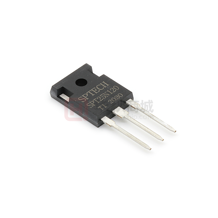
SPT25N120T1
1200V /25A Trench Field Stop IGBT
FEATURES
High breakdown voltage to 1200V for
VCE
1200
V
IC
25
A
VCE(SAT) IC=25A
1.65
V
improved reliability
Trench-Stop Technology offering :
Very tight parameter distribution
High ruggedness, temperature stable
behavior
Short circuit withstand time – 10s
Low VCE(SAT)
Easy parallel switching capability due
to positive temperature coefficient in
VCE(SAT)
Enhanced avalanche capability
APPLICATION
Frequency Converters
Motor Drive
Product
SPT25N120T1
http://www.superic-tech.com
Package
TO247
1
Packaging
Tube
2019.04 / Rev3.2
�SPT25N120T1
Maximum Ratings
Parameter
Symbol
Value
Unit
Collector-Emitter Breakdown Voltage
VCE
1200
V
DC collector current, limited by Tjmax
TC = 25°C
TC = 100°C
IC
50
25
A
Diode Forward current, limited by Tjmax
TC = 25°C
TC = 100°C
IF
50
25
A
Continuous Gate-emitter voltage
VGE
±20
V
Transient Gate-emitter voltage
VGE
±30
V
-
100
A
Pulsed collector current, VGE= 15V,
tp limited by Tjmax
ICM
100
A
Short Circuit Withstand Time, VGE= 15V,
VCE≤ 600V
Tsc
10
μs
Power dissipation , Tj=25℃
Ptot
250
W
Operating junction temperature
Tj
-40...+150
°C
Storage temperature
Ts
-55...+150
°C
Soldering temperature, wave soldering 1.6mm
(0.063in.) from case for 10s
-
260
°C
Turn off safe operating area VCE ≤1200V,
Tj ≤ 150°C
Thermal Resistance
Parameter
Symbol
Max. Value
IGBT thermal resistance,
junction - case
Rθ(j-c)
0.5
K/W
Diode thermal resistance,
junction - case
Rθ(j-c)
1
K/W
Thermal resistance,
junction - ambient
Rθ(j-a)
40
K/W
http://www.superic-tech.com
2
Unit
2019.04 / Rev3.2
�SPT25N120T1
Electrical Characteristics of the IGBT(Tj= 25℃ unless otherwise specified):
Parameter
Symbol
Conditions
Min
Typ
Max
Unit
Static
Collector-Emitter
breakdown voltage
BVCES
VGE=0V , IC=250μA
1200
-
-
V
Gate threshold voltage
VGE(th)
VGE=VCE, IC=250μA
5.2
6.0
6.8
V
Collector-Emitter
Saturation voltage
VCE(sat)
VGE=15V, IC=25A
Tj = 25°C
Tj = 150°C
-
1.65
2.0
2.05
-
V
Zero gate voltage
collector current
ICES
VCE = 1200V, VGE = 0V
Tj = 25°C
Tj = 150°C
-
-
100
1000
μA
-
Gate-emitter
leakage current
IGES
VCE = 0V, VGE = ±20V
-
-
100
nA
Transconductance
gfs
VCE=20V, IC=20A
-
20
-
S
Parameter
Symbol
Conditions
Min
Typ
Max
Unit
-
2340
-
-
105
-
-
60
-
VCC = 960V, IC = 25A,
VGE = 15V
-
135
-
nC
VGE=15V,tSC≤10us
VCC=600V,
Tj,start=25°C
-
210
-
A
Dynamic
Input capacitance
Cies
Output capacitance
Coes
Reverse transfer
capacitance
Cres
Gate charge
QG
Short circuit collector
current
IC(SC)
http://www.superic-tech.com
VCE = 25V, VGE = 0V,
f = 1MHz
3
2019.04 / Rev3.2
pF
�SPT25N120T1
Switching Characteristic, Inductive Load
Parameter
Symbol
Conditions
Min
Typ
Max
Unit
Dynamic , at Tj = 25°C
Turn-on delay time
td(on)
-
45
-
ns
tr
-
21
-
ns
-
2.2
-
mJ
-
200
-
ns
tf
-
93
-
ns
Eoff
-
0.75
-
mJ
Rise time
Turn-on energy
Turn-off delay time
VCC = 600V, IC = 25A,
VGE = 0/15V,
Rg=12Ω
Eon
td(off)
Fall time
Turn-off energy
Electrical Characteristics of the DIODE(Tj= 25℃
Parameter
Symbol
Conditions
unless otherwise specified)
Min
Typ
Max
Unit
-
3.0
-
V
-
180
-
ns
-
5
-
A
-
270
-
nC
Dynamic
Diode Forward Voltage
VFM
Reverse Recovery Time
Trr
Reverse Recovery Current
Irr
Reverse Recovery Charge
Qrr
http://www.superic-tech.com
IF = 25A
IF= 25A,
di/dt= 200A/μs
4
2019.04 / Rev3.2
�SPT25N120T1
Fig. 1 FBSOA characteristics
Fig. 2 Load Current vs. Frequency
100
100
90
80
80℃
70
tP = 10μs
50μs
10
60
100μs
IC(A)
IC(A)
500μs
1ms
DC
110℃
50
40
1
30
20
10
D=0.5, VCE=600V,
VGE=0/15V, Rg=12Ω,Tj ≤
150C
Ta=25°C, Tj ≤150C , VGE=15V
0
0
1
10
100
1
1000
10
Fig. 3 Output characteristics
Fig. 4 Saturation voltage characteristics
120
100
110
25℃
90
VGE = 20V
100
90
150℃
80
17V
15V
13V
80
70
11V
9V
7V
60
IC(A)
70
IC(A)
100
f (KHz)
VCE(V)
60
50
50
40
40
30
30
20
20
10
10
0
VGE = 15V
0
0
1
2
3
4
5
0
http://www.superic-tech.com
1
2
3
4
5
VCE(V)
VCE(V)
5
2019.04 / Rev3.2
6
�SPT25N120T1
Fig. 5 Switching times vs. gate resistor
Fig. 6 Switching times vs. collector current
1000
1000
td(off)
tf
td(on)
tr
t, SWITCHING TIMES [ns]
t, SWITCHING TIMES [ns]
td(off)
tf
td(on)
tr
100
100
Common Emitter
VCC = 600V, VGE = 15V, RG=12Ω
Ta=25℃
Common Emitter
VCC =600V, VGE = 15V, IC=25A
Ta=25℃
10
10
0
0 5 10 15 20 25 30 35 40 45 50 55 60 65
10
20
30
40
60
70
80
90
IC(A)
Rg (Ω)
Fig. 7 Switching loss vs. gate resistor
Fig. 8 Switching loss vs. collector current
3.5
16
Eon
Eoff
Eon
Eoff
14
3
12
Switching loss (mJ)
2.5
Switching loss (mJ)
50
2
1.5
10
Common Emitter
VCC = 600V, VGE = 15V, RG=12Ω
Ta=25℃
8
6
1
4
0.5
Common Emitter
VCC =600V, VGE = 15V, IC=25A
Ta=25℃
2
0
0
0 5 10 15 20 25 30 35 40 45 50 55 60 65
0
Rg (Ω)
http://www.superic-tech.com
10
20
30
40
50
60
70
80
90
Ic (A)
6
2019.04 / Rev3.2
�SPT25N120T1
Fig. 9 Gate charge characteristics
Fig. 10 Capacitance characteristics
10000
15
240V
640V
960V
12
Ciss(pF)
Coss(pF)
1000
Crss(pF)
Capacitance
VGE (V)
9
6
100
3
Common Emitter
VGE = 0V, f = 1MHz
Ta=25℃
Common Emitter
IC= 25A ,Ta=25℃
0
10
0
50
100
150
200
0
Qg (nC)
http://www.superic-tech.com
7
10
VCE(V)
20
2019.04 / Rev3.2
30
�SPT25N120T1
http://www.superic-tech.com
8
2019.04 / Rev3.2
�