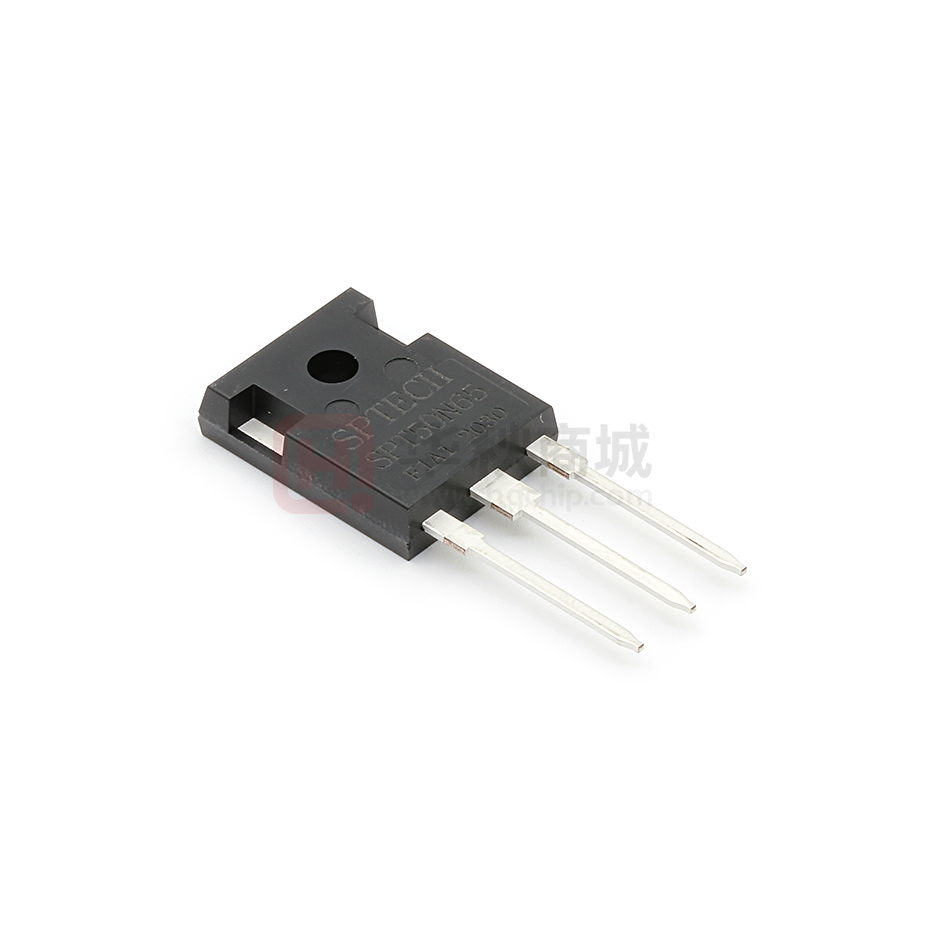
SPT50N65F1A1
650V /50A Trench Field Stop IGBT
650V Trench Field Stop IGBTs offer
VCE
650
V
and high avalanche ruggedness for motion
IC
50
A
control, solar application and welding machine.
VCE(SAT) IC=50A
1.65
V
low switching losses, high energy efficiency
FEATURES
High breakdown voltage up to 650V for
improved reliability
Trench-Stop Technology offering :
High speed switching
High ruggedness, temperature stable
Low VCEsat
Easy parallel switching capability due
to positive temperature coefficient in
VCEsat
Enhanced avalanche capability
APPLICATION
Uninterruptible Power Supplies
Inverter
Welding Converters
PFC applications
Converter with high switching frequency
Product
SPT50N65F1A1
Package
TO247
Packaging
Tube
http://www.superic-tech.com
1
2018.10 / Rev3.4
�SPT50N65F1A1
Maximum Ratings (Tj= 25℃ unless otherwise specified)
Parameter
Symbol
Value
Unit
Collector-Emitter Breakdown Voltage
VCE
650
V
DC collector current, limited by Tjmax
TC = 25°C
TC = 100°C
IC
100
50
A
Diode Forward current, limited by Tjmax
TC = 25°C
TC = 100°C
IF
100
50
A
200
A
260
W
-40...+150
°C
-55...+150
°C
260
°C
Turn off safe operating area VCE ≤650V,
Tj ≤ 150°C
Power dissipation , Tj=25℃
Ptot
Operating junction temperature Tj
Ts
Storage temperature
Soldering temperature, wave soldering
1.6mm (0.063in.) from case for 10s
Thermal Resistance
Parameter
Symbol
Max. Value
Unit
IGBT thermal resistance,
junction - case
Rθ(j-c)
0.48
K/W
Diode thermal resistance,
junction - case
Rθ(j-c)
1.1
K/W
Thermal resistance,
junction - ambient
Rθ(j-a)
40
K/W
http://www.superic-tech.com
2
2018.10 / Rev3.4
�SPT50N65F1A1
Electrical Characteristics (Tj= 25℃ unless otherwise specified)
Parameter
Symbol
Conditions
Min
Typ
Max
Unit
-
V
Static
VGE=0V , IC=250uA
650
VGE=0V , IC=1mA
650
VGE(th)
VGE=VCE, IC=250uA
4.0
VCE(sat)
VGE=15V, IC=50A
Tj = 25°C
Tj = 150°C
Collector-Emitter Breakdown
Voltage
BVCES
Gate Threshold Voltage
Collector-Emitter Saturation
Voltage
Zero gate voltage collector current
ICES
VCE = 650V, VGE = 0V
Tj = 25°C
Tj = 150°C
Gate-emitter leakage current
IGES
VCE = 0V, VGE = 20V
Transconductance
gfs
VCE = 20V, IC = 50A
Parameter
Symbol
Conditions
-
-
Min
V
5.0
6.0
V
1.65
2.05
2.0
V
V
0.1
40
1000
μA
100
nA
-
S
Max
Unit
50
Typ
Dynamic
Input capacitance
Cies
Output capacitance
Coes
Reverse transfer capacitance
Cres
Gate charge
QG
http://www.superic-tech.com
3800
VCE = 30V, VGE = 0V,
f = 1MHz
130
pF
70
VCC = 520V, IC = 50A,
VGE = 15V
3
-
162
-
nC
2018.10 / Rev3.4
�SPT50N65F1A1
Switching Characteristic, Inductive Load
Parameter
Symbol
Conditions
Min
Typ
Max
td(on)
-
60
-
tr
-
55
-
-
170
-
-
80
-
Unit
Dynamic Tj=25C
Turn-on Delay Time
Rise Time
Turn-off Delay Time
td(off)
Fall Time
tf
VCC = 400V, IC = 50.0A,
VGE = 0.0/15.0V,
Rg=12Ω
ns
ns
ns
ns
Turn-on Energy
Eon
-
2.2
-
mJ
Turn-off Energy
Eoff
-
0.6
-
mJ
td(on)
-
60
-
tr
-
60
-
-
172
-
-
90
-
Dynamic Tj=150C
Turn-on Delay Time
Rise Time
Turn-off Delay Time
td(off)
Fall Time
tf
VCC = 400V, IC = 50.0A,
VGE = 0.0/15.0V,
Rg=12Ω
ns
ns
ns
ns
Turn-on Energy
Eon
-
2.35
-
mJ
Turn-off Energy
Eoff
-
0.82
-
mJ
Max
Unit
Electrical Characteristics of the DIODE(Tj= 25℃ unless otherwise specified)
Parameter
Symbol
Conditions
Min
Typ
-
2.4
-
V
-
90
-
ns
-
17
-
A
-
900
-
nC
Dynamic
Diode Forward Voltage
VFM
Reverse Recovery Time
Trr
Reverse Recovery Current
Irr
Reverse Recovery Charge
Qrr
http://www.superic-tech.com
IF = 50A
IF= 40A,
VR = 300V,
di/dt= 600A/μs,
4
2018.10 / Rev3.4
�SPT50N65F1A1
Fig. 1 FBSOA characteristics
Fig. 2 Power dissipation as a function of TC
300
100
250
tP = 10μs
200
50μs
10
Ptot(W)
IC(A)
100μs
150
500μs
1ms
DC
100
1
50
Ta=25°C, Tj ≤150C , VGE=15V
0
0.1
1
10
100
25
1000
50
75
125
150
Fig. 4 Saturation voltage characteristics
200
VGE = 20V
180
150℃
17V
25℃
160
15V
140
13V
11V
120
9V
IC(A)
IC(A)
Fig. 3 Output characteristics
200
190
180
170
160
150
140
130
120
110
100
90
80
70
60
50
40
30
20
10
0
100
TC(℃)
VCE(V)
7V
100
80
60
40
20
VGE = 15V
0
0
1
2
3
4
5
0
VCE(V)
http://www.superic-tech.com
1
2
3
4
5
6
VCE(V)
5
2018.10 / Rev3.4
�SPT50N65F1A1
Fig. 5 Switching times vs. gate resistor
1000
Fig. 6 Switching times vs. collector current
1000
td(off)
td(off)
tf
tf
td(on)
td(on)
tr
t, SWITCHING TIMES [ns]
t, SWITCHING TIMES [ns]
tr
100
100
Common Emitter
VCC = 400V, VGE = 15V, IC=50A
Ta=25℃
Common Emitter
VCC = 400V, VGE = 15V, RG=12Ω
Ta=25℃
10
10
0
5 10 15 20 25 30 35 40 45 50 55 60 65
0
10 20 30 40 50 60 70 80 90 100 110
Rg (Ω)
IC(A)
Fig. 7 Switching loss vs. gate resistor
Fig. 8 Switching loss vs. collector current
4
4.5
Eoff
Eon
3.5
3.5
Switching loss (mJ)
3
Switching loss (mJ)
Eoff
Eon
4
2.5
2
1.5
3
2.5
2
1.5
1
1
0.5
Common Emitter
VCC = 400V, VGE = 15V, IC=50A
Ta=25℃
0
0
0
5 10 15 20 25 30 35 40 45 50 55 60 65
0
Rg (Ω)
http://www.superic-tech.com
Common Emitter
VCC = 400V, VGE = 15V,
RG=12Ω, Ta=25℃
0.5
10 20 30 40 50 60 70 80 90 100 110
Ic (A)
6
2018.10 / Rev3.4
�SPT50N65F1A1
Fig. 9 Gate charge characteristics
Fig. 10 Capacitance characteristics
10000
15
130V
520V
12
Ciss(pF)
Coss(pF)
1000
Crss(pF)
Capacitance
VGE (V)
9
6
100
3
Common Emitter
IC= 50A ,Ta=25℃
Common Emitter
VGE = 0V, f = 1MHz
Ta=25℃
0
10
0
50
100
150
200
0
Qg (nC)
http://www.superic-tech.com
10
20
30
VCE(V)
7
2018.10 / Rev3.4
�SPT50N65F1A1
http://www.superic-tech.com
8
2018.10 / Rev3.4
�