WST6003
P-Ch MOSFET
Product Summery
Features
D
D
D
D
D
D
D
TrenchFETr Power MOSFET: 1.8-V Rated
Gate-Source ESD Protected: 2000 V
High-Side Switching
Low On-Resistance: 1.2 W
Low Threshold: 0.8 V (typ)
Fast Switching Speed: 14 ns
S- Prefix for Automotive and Other Applications Requiring
Unique Site and Control Change Requirements; AEC-Q101
Qualified and PPAP Capable.
BVDSS
RDSON
ID
-20V
1200mΩ
-0.35A
Applications
D Drivers: Relays, Solenoids, Lamps, Hammers,
Displays, Memories
D Battery Operated Systems
D Power Supply Converter Circuits
D Load/Power Switching Cell Phones, Pagers
BENEFITS
D
D
D
D
D
SOT-523 Pin Configuration
Ease in Driving Switches
Low Offset (Error) Voltage
Low-Voltage Operation
High-Speed Circuits
Low Battery Voltage Operation
3 Drain
1
2
Gate
Source
Absolute Maximum Ratings
Symbol
Parameter
Rating
Units
VDS
Drain-Source Voltage
-20
V
VGS
Gate-Source Voltage
±6
V
ID@Tc=25℃
Continuous Drain Current, VGS @ -4.5V1
-0.35
A
ID@Tc=70℃
1
-0.4
A
-1
A
IDM
Continuous Drain Current, VGS @ -4.5V
Pulsed Drain Current
2
PD@TA=25℃
Total Power Dissipation
0.15
W
TSTG
Storage Temperature Range
-55 to 150
℃
TJ
Operating Junction Temperature Range
-55 to 150
℃
3
Thermal Data
Symbol
Parameter
RθJA
Thermal Resistance Junction-ambient
RθJC
Thermal Resistance Junction-Case1
www.winsok.tw
Page 1
1
Typ.
Max.
Unit
---
125
℃/W
---
80
℃/W
Dec.2014
�WST6003
P-Ch MOSFET
Electrical Characteristics (TJ=25 ℃, unless otherwise noted)
Symbol
BVDSS
Parameter
Drain-Source Breakdown Voltage
△BVDSS/△TJ BVDSS Temperature Coefficient
Conditions
Min.
Typ.
Max.
Unit
VGS=0V , ID=-250uA
-20
---
---
V
Reference to 25℃ , ID=-1mA
---
-0.016
---
V/℃
---
0.8
1.2
VGS=-2.5V , ID=-0.3A
---
1.2
1.6
VGS=-1.8V , ID=-0.01A
---
1.8
2.7
-0.45
---
---
V
---
3.97
---
mV/℃
VDS=-16V , VGS=0V , TJ=25℃
---
---
-1
VDS=-16V , VGS=0V , TJ=55℃
---
---
-5
VGS=-4.5V , ID=-0.35A
RDS(ON)
VGS(th)
Static Drain-Source On-Resistance2
Gate Threshold Voltage
VGS=VDS , ID =-250uA
Ω
△VGS(th)
VGS(th) Temperature Coefficient
IDSS
Drain-Source Leakage Current
IGSS
Gate-Source Leakage Current
VGS=±8V , VDS=0V
---
---
±100
nA
gfs
Forward Transconductance
VDS=-5V , ID=-1A
---
6.2
---
S
Rg
Gate Resistance
VDS=0V , VGS=0V , f=1MHz
---
9.5
12
Ω
---
1500
---
---
150
---
Gate-Drain Charge
---
450
---
Turn-On Delay Time
---
5
---
Qg
Qgs
Qgd
Td(on)
Tr
Td(off)
Tf
Total Gate Charge (-4.5V)
Gate-Source Charge
VDS=-15V , VGS=-4.5V , ID=-1A
Rise Time
VDD=-15V , VGS=-4.5V ,
---
9
---
Turn-Off Delay Time
RG=3.3Ω ID=-1A
---
35
---
---
11
---
Fall Time
uA
pC
ns
Notes
a. Pulse test; pulse width v 300 ms, duty cycle v 2%.
b. Guaranteed by design, not subject to production testing.
www.winsok.tw
Page 2
Dec.2014
�WST6003
P-Ch MOSFET
Typical Characteristics
For the following graphs, p-channel negative polarities for all voltage and current values are represented as positive values.
Output Characteristics
Transfer Characteristics
1.0
1000
VGS = 5 thru 3 V
TJ = –55_C
2.5 V
25_C
800
I D – Drain Current (mA)
I D – Drain Current (A)
0.8
0.6
2V
0.4
1.8 V
0.2
600
125_C
400
200
0.0
0.0
0.5
1.0
1.5
2.0
2.5
0
0.0
3.0
0.5
VDS – Drain-to-Source Voltage (V)
1.0
2.5
3.0
Capacitance
4.0
120
100
3.2
C – Capacitance (pF)
r DS(on) – On-Resistance ( W )
2.0
VGS – Gate-to-Source Voltage (V)
On-Resistance vs. Drain Current
VGS = 1.8 V
2.4
VGS = 2.5 V
1.6
VGS = 4.5 V
Ciss
80
60
40
Coss
0.8
20
0.0
Crss
0
0
200
400
600
800
1000
0
4
ID – Drain Current (mA)
Gate Charge
12
16
20
On-Resistance vs. Junction Temperature
1.6
r DS(on) – On-Resistance (W)
(Normalized)
VDS = 10 V
ID = 250 mA
4
3
2
1
0
0.0
8
VDS – Drain-to-Source Voltage (V)
5
V GS – Gate-to-Source Voltage (V)
1.5
1.4
VGS = 4.5 V
ID = 350 mA
1.2
VGS = 1.8 V
ID = 150 mA
1.0
0.8
0.2
0.4
0.6
0.8
1.0
1.2
1.4
0.6
–50
1.6
www.winsok.tw
–25
0
25
50
75
100
125
TJ – Junction Temperature_( C)
Qg – Total Gate Charge (nC)
Page 3
Dec.2014
�WST6003
P-Ch MOSFET
Typical Characteristics
Source-Drain Diode Forward Voltage
On-Resistance vs. Gate-to-Source Voltage
5
TJ = 125_C
r DS(on) – On-Resistance ( W )
IS – Source Current (mA)
1000
100
TJ = 25_C
TJ = –55_C
10
1
0.0
4
3
ID = 350 mA
2
ID = 200 mA
1
0
0.2
0.4
0.6
0.8
1.0
1.2
1.4
0
1
VSD – Source-to-Drain Voltage (V)
VGS – Gate-to-Source Voltage (V)
IGSS vs. Temperature
3.0
0.2
2.5
ID = 0.25 mA
0.1
2.0
IGSS – (mA)
V GS(th) Variance (V)
Threshold Voltage Variance vs. Temperature
0.3
–0.0
1.5
–0.1
1.0
–0.2
0.5
–0.3
–50
–25
0
25
50
75
100
0.0
–50
125
VGS = 4.5 V
–25
TJ – Temperature (_C)
0
25
50
75
100
125
TJ – Temperature (_C)
BVGSS – Gate-to-Source Breakdown Voltage (V)
BVGSS vs. Temperature
7
6
5
4
3
2
1
0
–50
–25
0
25
50
75
100
125
TJ – Temperature (_C)
www.winsok.tw
Page 4
Dec.2014
�WST6003
P-Ch MOSFET
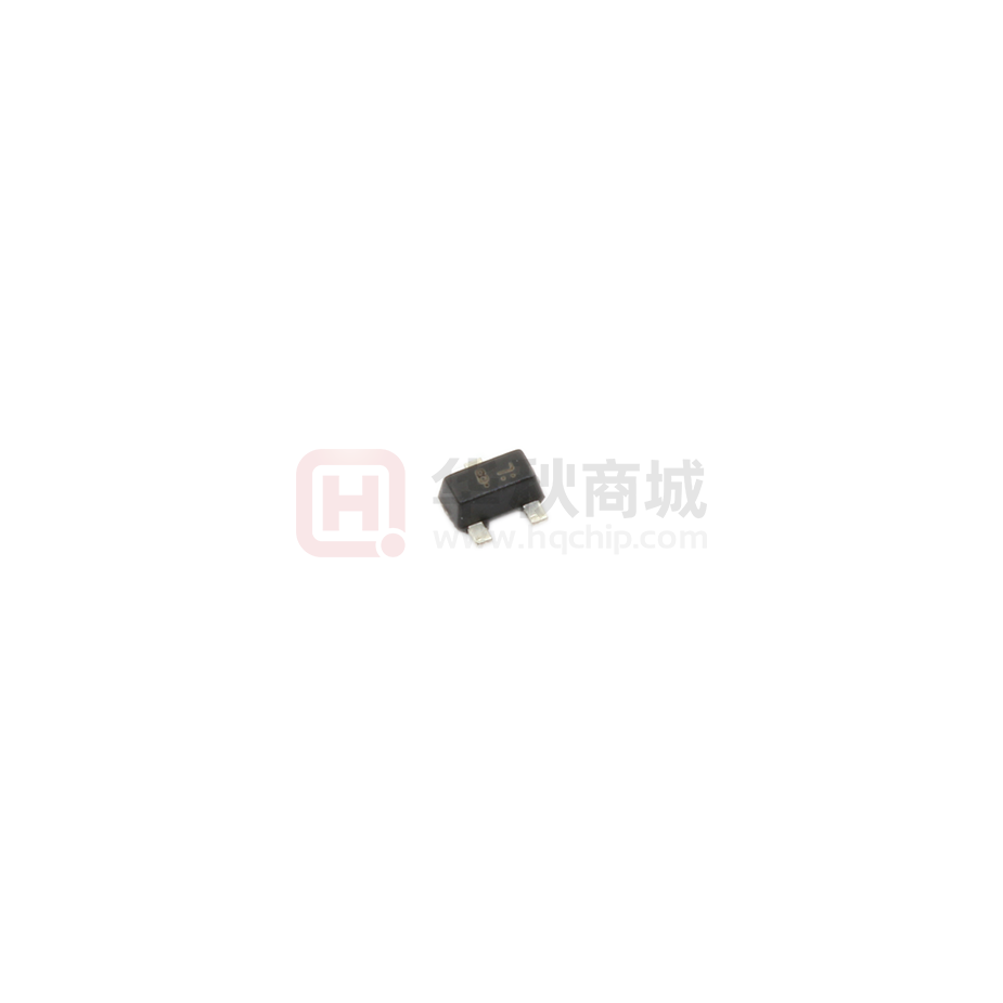
SOT-523
www.winsok.tw
Page 5
Dec.2014
�Attention�
1,�Any�and�all�Winsok�power�products�described�or�contained�herein�do�not�have�specifications�that�can�handle�
applications�that�require�extremely�high�levels�of�reliability,�such�as�lifeͲsupport�systems,�aircraft's�control�systems,�or�
other�applications�whose�failure�can�be�reasonably�expected�to�result�in�serious�physical�and/or�material�damage.� �
Consult�with�your�Winsok�power�representative�nearest�you�before�using�any�Winsok�power�products�described�or�
contained�herein�in�such�applications.�
2,Winsok�power�assumes�no�responsibility�for�equipment�failures�that�result�from�using�products�at�values�that�exceed,� �
even�momentarily,�rated�values�(such�as�maximum�ratings,�operating�condition�ranges,�or�other�parameters)�listed�in�
products�specifications�of�any�and�all�Winsok�power�products�described�or�contained�herein.�
3,�Specifications�of�any�and�all�Winsok�power�products�described�or�contained�herein�stipulate�the�performance,�
characteristics,�and�functions�of�the�described�products�in�the�independent�state,�and�are�not�guarantees�of�the�
performance,�characteristics,�and�functions�of�the�described�products�as�mounted�in�the�customer’s�products�or�
equipment.�To�verify�symptoms�and�states�that�cannot�be�evaluated�in�an�independent�device,�the�customer�should�always�
evaluate�and�test�devices�mounted�in�the�customer’s�products�or�equipment.�
4,�Winsok�power�Semiconductor�CO.,�LTD.�strives�to�supply�highͲquality�highͲreliability�products.�However,�any�and�all�
semiconductor�products�fail�with�some�probability.�It�is�possible�that�these�probabilistic�failures�could�give�rise�to�accidents�
or�events�that�could�endanger�human�lives�that�could�give�rise�to�smoke�or�fire,�or�that�could�cause�damage�to�other�
property.�When�designing�equipment,�adopt�safety�measures�so�that�these�kinds�of�accidents�or�events�cannot�occur.�Such�
measures�include�but�are�not�limited�to�protective�circuits�and�error�prevention�circuits�for�safe�design,�redundant�design,�
and�structural�design.�
5,In�the�event�that�any�or�all�Winsok�power�products(including�technical�data,�services)�described�or�contained�herein�are�
controlled�under�any�of�applicable�local�export�control�laws�and�regulations,�such�products�must�not�be�exported�without�
obtaining�the�export�license�from�the�authorities�concerned�in�accordance�with�the�above�law.�
6,�No�part�of�this�publication�may�be�reproduced�or�transmitted�in�any�form�or�by�any�means,�electronic�or�mechanical,�
including�photocopying�and�recording,�or�any�information�storage�or�retrieval�system,�or�otherwise,�without�the�prior�
written�permission�of�Winsok�power�Semiconductor�CO.,�LTD.�
7,�Information�(including�circuit�diagrams�and�circuit�parameters)�herein�is�for�example�only;�it�is�not�guaranteed�for�
volume�production. Winsok�power�believes�information�herein�is�accurate�and�reliable,�but�no�guarantees�are�made�or�
implied�regarding�its�use�or�any�infringements�of�intellectual�property�rights�or�other�rights�of�third�parties.�
8,�Any�and�all�information�described�or�contained�herein�are�subject�to�change�without�notice�due�to�product/technology�
improvement,etc.�When�designing�equipment,�refer�to�the�"Delivery�Specification"�for�the�Winsok�power�product�that�you� �
Intend�to�use.�
9,�this�catalog�provides�information�as�of�Sep.2014. Specifications�and�information�herein�are�subject�to�change�without�
notice.�
�