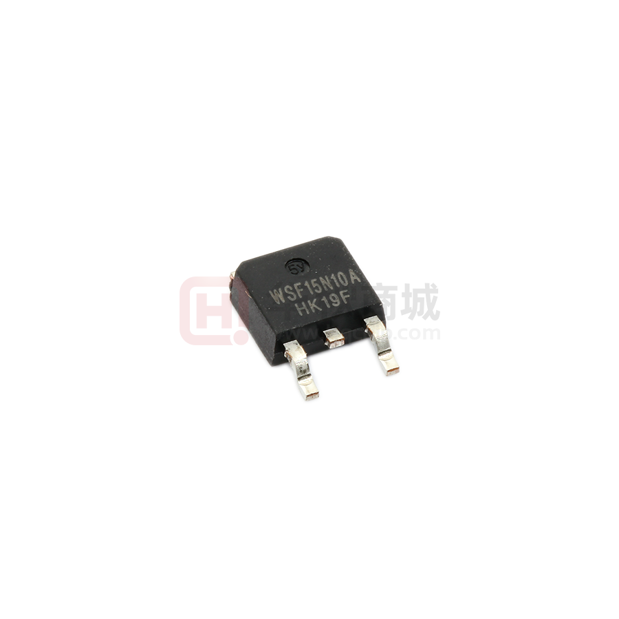
WSF15N10A
N-Ch MOSFET
Product Summery
General Description
The WSF15N10A uses advanced trench technology and
design to provide excellent RDS(ON) with low gate charge. It
BVDSS
RDSON
ID
100V
90mΩ
15A
can be used in a wide variety of applications.
Features
● High density cell design for ultra low Rdson
TO-252 Pin Configuration
● Fully characterized avalanche voltage and current
● Good stability and uniformity with high EAS
● Excellent package for good heat dissipation
● Special process technology for high ESD capability
Application
● Power switching application
● Hard switched and high frequency circuits
● Uninterruptible power supply
Absolute Maximum Ratings
Symbol
Parameter
Rating
Units
VDS
Drain-Source Voltage
100
V
VGS
Gate-Source Voltage
ID@TC=25℃
ID@TC=100℃
±20
V
1
15
A
1
7
A
40
A
Continuous Drain Current, VGS @ 10V
Continuous Drain Current, VGS @ 10V
2
IDM
PD@TC=25℃
Pulsed Drain Current
Maximum Power Dissipation
40
W
0.27
W/℃
Single Pulse Avalanche Energy
20
mJ
Operating Junction Temperature Range
-55 to 170
℃
Derating factor
3
EAS
TJ
TSTG
Thermal Data
Symbol
Parameter
RθJA
Thermal Resistance Junction-ambient
RθJC
1
www.winsok.tw
Thermal Resistance Junction-Case
Page 1
1
Typ.
Max.
Unit
---
50
℃/W
---
3.8
℃/W
Dec.2014
�WSF15N10A
N-Ch MOSFET
Electrical Characteristics (TJ=25 ℃, unless otherwise noted)
Symbol
BVDSS
Parameter
Conditions
Drain-Source Breakdown Voltage
=
VGS=0V , ID 250uA
△BVDSS/△TJ BVDSS Temperature Coefficient
RDS(ON)
Reference to 25℃ , ID=1mA
Static Drain-Source On-Resistance2
=
VGS=10V , ID 5A
Min.
Typ.
Max.
Unit
100
---
---
V
---
0.098
---
V/℃
---
90
110
mΩ
150
mΩ
---
110
Gate Threshold Voltage
VGS=VDS , ID =250uA
1.0
1.5
2.5
IDSS
IGSS
Drain-Source Leakage Current
Gate-Source Leakage Current
VDS=80V , VGS=0V , TJ=25℃
---
---
1
V
nA
VGS=±20V , VDS=0V
---
---
±100
uA
gfs
Forward Transconductance
3.5
---
---
S
VGS(th)
=
VDS=5V , ID 5A
---
21.5
---
---
3.2
---
Gate-Drain Charge
---
6.0
---
Turn-On Delay Time
---
11
24
Qg
Total Gate Charge (10V)
Qgs
Gate-Source Charge
Qgd
Td(on)
=
VGS=4.5V , ID 2A
VDS=50V , VGS=10V , ID=5A
nC
Rise Time
VDD=30V , VGS=10V , RG=6Ω
---
7.4
15
Turn-Off Delay Time
ID=1A , RL=30Ω
---
35
45
Fall Time
---
9.1
12
Ciss
Input Capacitance
---
730
---
Coss
Output Capacitance
---
37
---
Crss
Reverse Transfer Capacitance
---
27
---
Min.
Typ.
Max.
Unit
VG=VD=0V , Force Current
---
---
10
A
VGS=0V , IS=10A , TJ=25℃
---
---
1.2
V
17
21
61
nS
61
97
113
nC
Tr
Td(off)
Tf
VDS=30V , VGS=0V , f=1MHz
ns
pF
Diode Characteristics
Symbol
IS
Parameter
Continuous Source Current
2
VSD
Diode Forward Voltage
trr
Reverse Recovery Time
Qrr
Reverse Recovery Charge
Conditions
IF=10A , dI/dt=100A/µs , TJ=25℃
Notes:
1. Repetitive Rating: Pulse width limited by maximum junction temperature.
2. Surface Mounted on FR4 Board, t ≤ 10 sec.
3. Pulse Test: Pulse Width ≤ 300μs, Duty Cycle ≤ 2%.
4. Guaranteed by design, not subject to production
5. EAS condition:Tj=25℃,VDD=50V,VG=10V,L=0.5mH,Rg=25
www.winsok.tw
Page 2
Dec.2014
�WSF15N10A
N-Ch MOSFET
ID- Drain Current (A)
Normalized On-Resistance
Typical Characteristics
TJ-Junction Temperature(℃)
Vds Drain-Source Voltage (V)
Figure 4 Rdson-JunctionTemperature
ID- Drain Current (A)
Vgs Gate-Source Voltage (V)
Figure 1 Output Characteristics
Qg Gate Charge (nC)
Figure 2 Transfer Characteristics
Figure 5 Gate Charge
Is- Reverse Drain Current (A)
Rdson On-Resistance(mΩ)
Vgs Gate-Source Voltage (V)
ID- Drain Current (A)
Figure 3 Rdson- Drain Current
www.winsok.tw
Vsd Source-Drain Voltage (V)
Figure 6 Source- Drain Diode Forward
Page 3
Dec.2014
�WSF15N10A
C Capacitance (pF)
Power Dissipation (W)
N-Ch MOSFET
TJ-Junction Temperature(℃)
Figure 7 Capacitance vs Vds
Figure 9 Power De-rating
ID- Drain Current (A)
ID- Drain Current (A)
Vds Drain-Source Voltage (V)
TJ-Junction Temperature(℃)
Figure 8 Safe Operation Area
Figure 10 Current De-rating
r(t),Normalized Effective
Transient Thermal Impedance
Vds Drain-Source Voltage (V)
Square Wave Pluse Duration(sec)
Figure 11 Normalized Maximum Transient Thermal Impedance
www.winsok.tw
Page 4
Dec.2014
�Attention�
1,�Any�and�all�Winsok�power�products�described�or�contained�herein�do�not�have�specifications�that�can�handle�
applications�that�require�extremely�high�levels�of�reliability,�such�as�lifeͲsupport�systems,�aircraft's�control�systems,�or�
other�applications�whose�failure�can�be�reasonably�expected�to�result�in�serious�physical�and/or�material�damage.� �
Consult�with�your�Winsok�power�representative�nearest�you�before�using�any�Winsok�power�products�described�or�
contained�herein�in�such�applications.�
2,Winsok�power�assumes�no�responsibility�for�equipment�failures�that�result�from�using�products�at�values�that�exceed,� �
even�momentarily,�rated�values�(such�as�maximum�ratings,�operating�condition�ranges,�or�other�parameters)�listed�in�
products�specifications�of�any�and�all�Winsok�power�products�described�or�contained�herein.�
3,�Specifications�of�any�and�all�Winsok�power�products�described�or�contained�herein�stipulate�the�performance,�
characteristics,�and�functions�of�the�described�products�in�the�independent�state,�and�are�not�guarantees�of�the�
performance,�characteristics,�and�functions�of�the�described�products�as�mounted�in�the�customer’s�products�or�
equipment.�To�verify�symptoms�and�states�that�cannot�be�evaluated�in�an�independent�device,�the�customer�should�always�
evaluate�and�test�devices�mounted�in�the�customer’s�products�or�equipment.�
4,�Winsok�power�Semiconductor�CO.,�LTD.�strives�to�supply�highͲquality�highͲreliability�products.�However,�any�and�all�
semiconductor�products�fail�with�some�probability.�It�is�possible�that�these�probabilistic�failures�could�give�rise�to�accidents�
or�events�that�could�endanger�human�lives�that�could�give�rise�to�smoke�or�fire,�or�that�could�cause�damage�to�other�
property.�When�designing�equipment,�adopt�safety�measures�so�that�these�kinds�of�accidents�or�events�cannot�occur.�Such�
measures�include�but�are�not�limited�to�protective�circuits�and�error�prevention�circuits�for�safe�design,�redundant�design,�
and�structural�design.�
5,In�the�event�that�any�or�all�Winsok�power�products(including�technical�data,�services)�described�or�contained�herein�are�
controlled�under�any�of�applicable�local�export�control�laws�and�regulations,�such�products�must�not�be�exported�without�
obtaining�the�export�license�from�the�authorities�concerned�in�accordance�with�the�above�law.�
6,�No�part�of�this�publication�may�be�reproduced�or�transmitted�in�any�form�or�by�any�means,�electronic�or�mechanical,�
including�photocopying�and�recording,�or�any�information�storage�or�retrieval�system,�or�otherwise,�without�the�prior�
written�permission�of�Winsok�power�Semiconductor�CO.,�LTD.�
7,�Information�(including�circuit�diagrams�and�circuit�parameters)�herein�is�for�example�only;�it�is�not�guaranteed�for�
volume�production. Winsok�power�believes�information�herein�is�accurate�and�reliable,�but�no�guarantees�are�made�or�
implied�regarding�its�use�or�any�infringements�of�intellectual�property�rights�or�other�rights�of�third�parties.�
8,�Any�and�all�information�described�or�contained�herein�are�subject�to�change�without�notice�due�to�product/technology�
improvement,etc.�When�designing�equipment,�refer�to�the�"Delivery�Specification"�for�the�Winsok�power�product�that�you� �
Intend�to�use.�
9,�this�catalog�provides�information�as�of�Sep.2014. Specifications�and�information�herein�are�subject�to�change�without�
notice.�
�