WST2004
N-Ch MOSFET
Features
Product Summery
BVDSS
RDSON (TYP.)
z Lead Free Product is Acquired
z Surface Mount Package
z N-Channel Switch with Low RDS(on)
20V
240mΩ
20V
280mΩ
z Operated at Low Logic Level Gate Drive
20V
410mΩ
20V
450mΩ
ID (MAX)
0.6A
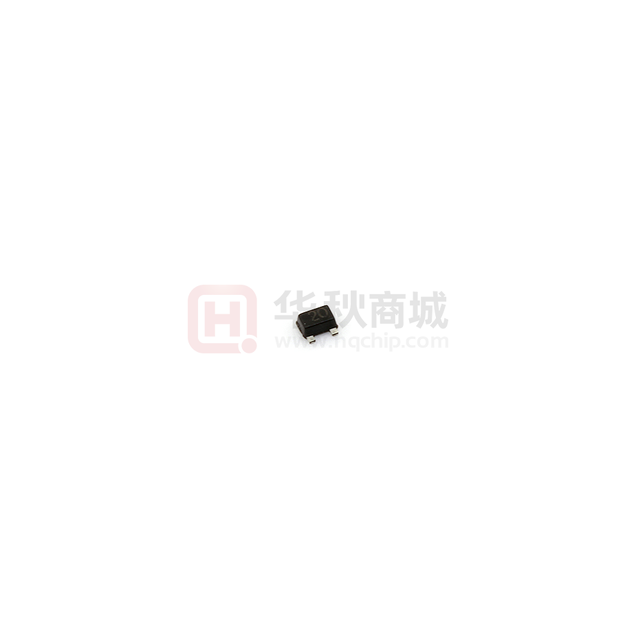
SOT-723 Pin Configuration
Applications
D
3
z Load/Power Switching
z Interfacing Switching
z Battery Management for Ultra Small
Portable Electronics
z Logic Level Shift
1
2
G
S
Absolute Maximum Ratings
Symbol
Parameter
Rating
Units
VDS
Drain-Source Voltage
20
V
VGS
Gate-Source Voltage
±8
V
400
mA
1.2
A
Total Power Dissipation
0.150
W
℃/W
ID@TA=25℃
IDM
PD@TA=25℃
RθJA
1
Continuous Drain Current, VGS @ 10V
Pulsed Drain Current
2
3
Thermal Resistance from Junction to Ambient (note 1)
823
TJ
Junction Temperature
150
℃
TSTG
Storage Temperature Range
-55 to 150
℃
TL
Lead Temperature for Soldering Purposes(1/8” from case for 10 s)
260
℃
www.winsok.tw
Page 1
Dec.2014
�WST2004
N-Ch MOSFET
Electrical Characteristics (TJ=25 ℃, unless otherwise noted)
Symbol
BVDSS
Parameter
Conditions
Drain-Source Breakdown Voltage
△BVDSS/△TJ BVDSS Temperature Coefficient
RDS(ON)
VGS(th)
Static Drain-Source On-Resistance
Gate Threshold Voltage
Min.
Typ.
Max.
Unit
VGS=0V , ID=250uA
20
---
---
V
Reference to 25℃ , ID=1mA
---
0.05
---
V/℃
VGS=4.5V , ID=0.4A
---
240
450
VGS=2.5V , ID=0.3A
---
280
765
VGS=1.8V , ID=0.2A
---
410
850
VGS=1.5V , ID=0.1A
---
450
950
0.35
---
1.0
V
---
-3.7
---
mV/℃
VDS=16V , VGS=0V , TJ=25℃
---
---
1
VDS=16V , VGS=0V , TJ=55℃
---
---
5
±10
VGS=VDS , ID =250uA
△VGS(th)
VGS(th) Temperature Coefficient
IDSS
Drain-Source Leakage Current
IGSS
Gate-Source Leakage Current
VGS=±8V , VDS=0V
---
---
gfs
Forward Transconductance
VDS=5V , ID=0.1A
---
1.5
-----
mΩ
mΩ
uA
uA
S
---
5.8
Rise Time
VDD=15V , VGS=10V ,
---
2.9
---
Turn-Off Delay Time
RG=6Ω, ID=0.1A
---
18
---
Fall Time
---
9
---
Ciss
Input Capacitance
---
88
---
Coss
Output Capacitance
---
15
---
Crss
Reverse Transfer Capacitance
---
10
---
Min.
Typ.
Max.
Unit
---
---
100
mA
---
---
0.5
A
---
---
1.2
V
Td(on)
Tr
Td(off)
Tf
Turn-On Delay Time
VDS=15V , VGS=0V , f=1MHz
ns
pF
Diode Characteristics
Symbol
IS
ISM
VSD
Parameter
Conditions
1,4
Continuous Source Current
2,4
Pulsed Source Current
2
Diode Forward Voltage
VG=VD=0V , Force Current
VGS=0V , IS=0.2A , TJ=25℃
Notes :
1.. Surface mounted on FR4 board using the minimum recommended pad size.
2. Pulse Test : Pulse Width=300µs, Duty Cycle=2%.
3. Switching characteristics are independent of operating junction temperatures.
4. Guaranteed by design, not subject to producting.
www.winsok.tw
Page 2
Dec.2014
�WST2004
N-Ch MOSFET
Typical Performance Characteristics
Output Characteristics
Transfer Characteristics
5.0
4.5
4.0
VGS=4V,5V
Ta=25℃
VDS=3V
VGS=3V
3.5
VGS=2.5V
3.0
Pulsed
Pulsed
(A)
ID
3.5
3.0
DRAIN CURRENT
DRAIN CURRENT
ID
(A)
4.0
VGS=2V
2.5
2.0
1.5
Ta=25℃
2.5
Ta=100℃
2.0
1.5
1.0
VGS=1.5V
1.0
0.5
0.5
0.0
0.0
0.0
0.5
1.0
1.5
2.0
2.5
3.0
3.5
DRAIN TO SOURCE VOLTAGE
4.0
VDS
4.5
5.0
0
(V)
1
2
GATE TO SOURCE VOLTAGE
3
VGS
4
(V)
RDS(ON) —— VGS
RDS(ON) —— ID
500
800
Ta=25℃
Pulsed
Pulsed
700
(m)
400
350
VGS=2.5V
300
VGS=4.5V
500
250
200
0.1
ID=0.65A
600
ON-RESISTANCE
ON-RESISTANCE
RDS(ON)
(m)
VGS=1.8V
RDS(ON)
450
Ta=100℃
400
300
Ta=25℃
200
100
0.2
0.3
0.4
0.5
0.6
0.7
DRAIN CURRENT
0.8
ID
0.9
1.0
1.1
1.2
1
(A)
2
3
4
GATE TO SOURCE VOLTAGE
GS
5
(V)
Threshold Voltage
IS —— VSD
2
0.8
Pulsed
1
VTH
Ta=100℃
0.1
THRESHOLD VOLTAGE
SOURCE CURRENT
IS (A)
(V)
0.7
Ta=25℃
0.6
ID=250uA
0.5
0.4
0.3
0.01
0.0
0.2
0.4
0.6
0.8
1.0
SOURCE TO DRAIN VOLT
VOLTAGE
A
www.winsok.tw
1.2
SD
1.4
1.6
0.2
25
(V)
50
75
JUNCTION TEMPERATURE
Page 3
100
Tj
125
(℃ )
Dec.2014
�WST2004
N-Ch MOSFET
SOT-723 Package Outline Dimensions
Symbol
A
A1
b
b1
c
D
E
E1
e
θ
Dimensions In Millimeters
Min.
Max.
0.430
0.500
0.000
0.050
0.170
0.270
0.270
0.370
0.080
0.150
1.150
1.250
1.150
1.250
0.750
0.850
0.800TYP.
7° REF.
Dimensions In Inches
Min.
Max.
0.017
0.020
0.000
0.002
0.007
0.011
0.011
0.015
0.003
0.006
0.045
0.049
0.045
0.049
0.030
0.033
0.031TYP.
7° REF.
SOT-723 Suggested Pad Layout
www.winsok.tw
Page 4
Dec.2014
�Attention�
1,�Any�and�all�Winsok�power�products�described�or�contained�herein�do�not�have�specifications�that�can�handle�
applications�that�require�extremely�high�levels�of�reliability,�such�as�lifeͲsupport�systems,�aircraft's�control�systems,�or�
other�applications�whose�failure�can�be�reasonably�expected�to�result�in�serious�physical�and/or�material�damage.� �
Consult�with�your�Winsok�power�representative�nearest�you�before�using�any�Winsok�power�products�described�or�
contained�herein�in�such�applications.�
2,Winsok�power�assumes�no�responsibility�for�equipment�failures�that�result�from�using�products�at�values�that�exceed,� �
even�momentarily,�rated�values�(such�as�maximum�ratings,�operating�condition�ranges,�or�other�parameters)�listed�in�
products�specifications�of�any�and�all�Winsok�power�products�described�or�contained�herein.�
3,�Specifications�of�any�and�all�Winsok�power�products�described�or�contained�herein�stipulate�the�performance,�
characteristics,�and�functions�of�the�described�products�in�the�independent�state,�and�are�not�guarantees�of�the�
performance,�characteristics,�and�functions�of�the�described�products�as�mounted�in�the�customer’s�products�or�
equipment.�To�verify�symptoms�and�states�that�cannot�be�evaluated�in�an�independent�device,�the�customer�should�always�
evaluate�and�test�devices�mounted�in�the�customer’s�products�or�equipment.�
4,�Winsok�power�Semiconductor�CO.,�LTD.�strives�to�supply�highͲquality�highͲreliability�products.�However,�any�and�all�
semiconductor�products�fail�with�some�probability.�It�is�possible�that�these�probabilistic�failures�could�give�rise�to�accidents�
or�events�that�could�endanger�human�lives�that�could�give�rise�to�smoke�or�fire,�or�that�could�cause�damage�to�other�
property.�When�designing�equipment,�adopt�safety�measures�so�that�these�kinds�of�accidents�or�events�cannot�occur.�Such�
measures�include�but�are�not�limited�to�protective�circuits�and�error�prevention�circuits�for�safe�design,�redundant�design,�
and�structural�design.�
5,In�the�event�that�any�or�all�Winsok�power�products(including�technical�data,�services)�described�or�contained�herein�are�
controlled�under�any�of�applicable�local�export�control�laws�and�regulations,�such�products�must�not�be�exported�without�
obtaining�the�export�license�from�the�authorities�concerned�in�accordance�with�the�above�law.�
6,�No�part�of�this�publication�may�be�reproduced�or�transmitted�in�any�form�or�by�any�means,�electronic�or�mechanical,�
including�photocopying�and�recording,�or�any�information�storage�or�retrieval�system,�or�otherwise,�without�the�prior�
written�permission�of�Winsok�power�Semiconductor�CO.,�LTD.�
7,�Information�(including�circuit�diagrams�and�circuit�parameters)�herein�is�for�example�only;�it�is�not�guaranteed�for�
volume�production. Winsok�power�believes�information�herein�is�accurate�and�reliable,�but�no�guarantees�are�made�or�
implied�regarding�its�use�or�any�infringements�of�intellectual�property�rights�or�other�rights�of�third�parties.�
8,�Any�and�all�information�described�or�contained�herein�are�subject�to�change�without�notice�due�to�product/technology�
improvement,etc.�When�designing�equipment,�refer�to�the�"Delivery�Specification"�for�the�Winsok�power�product�that�you� �
Intend�to�use.�
9,�this�catalog�provides�information�as�of�Sep.2014. Specifications�and�information�herein�are�subject�to�change�without�
notice.�
�