DMG1012T

DMG1012T

  • 厂商:

    YENJI(台湾元基)

  • 封装:

    SOT-523-3

  • 描述:

    MOSFET SOT523 Dual N-Channel ID=650mA

  • 详情介绍
  • 数据手册
  • 价格&库存
DMG1012T 数据手册
DMG1012T Dual N Channel Enhancement Mode MOSFET 0.65A DESCRIPTION DMG1012T N1012 is the N-Channel enhancement mode power field effect transistors are produced using high cell density, DMOS trench technology. This high density process is especially tailored to minimize on-state resistance and provide superior switching performance. These devices are particularly suited for low voltage applications such as notebook computer power management and other bettery powered circuits where high-side switching, low in-line power loss, and resistance to transients are needed. PIN CONFIGURATION 523 / SC89 SOTSOT-523 SC-89 FEATURE � � � � � � 20V/0.65A, RDS(ON) =380ohm@VGS =4.5V 20V/0.55A, RDS(ON) =450ohm@VGS =2.5V 20V/0.45A, RDS(ON) =800ohm@VGS =1.8V Super high density cell design for extremely low RDS(ON) Exceptional low on-resistance and maximum DC current capability SOT-523 / SC89 package design 1/6 DMG1012T Dual N Channel Enhancement Mode MOSFET 0.65A ABSOULTE MAXIMUM RATINGS (Ta = 25℃ Unless otherwise noted ) Parameter Symbol Typical Unit Drain-Source Voltage VDSS 20 V Gate-Source Voltage VGSS +/-12 V TA=25℃ Continuous Drain Current (TJ=150℃) TA=80℃ Pulsed Drain Current Continuous Source Current (Diode Conduction) 0.65 ID 1.0 A IS 0.3 A PD Storage Temperature Range 2/6 0.27 W 0.16 TA=70℃ Operation Junction Temperature A IDM TA=25℃ Power Dissipation 0.45 TJ -55/150 ℃ TSTG -55/150 ℃ DMG1012T Dual N Channel Enhancement Mode MOSFET 0.65A ELECTRICAL CHARACTERISTICS ( Ta = 25℃ Unless otherwise noted ) Parameter Symbol Condition Min Typ Max Unit OFF CHARACTERISTICS Drain-Source Breakdown Voltage Gate Threshold Voltage V(BR)DSS VGS=0V,ID=250uA VGS(th) VDS=VGS,ID=250uA Gate Leakage Current IGSS Zero Gate Voltage Drain Current IDSS On-State Drain Current ID(on) Drain-source On-Resistance Forward Transconductance RDS(on) gfs Diode Forward Voltage VSD DYNAMIC Total Gate Charge Qg Gate-Source Charge Qgs Gate-Drain Charge Qgd Turn-On Time Turn-Off Time Td(on) tr Td(off) tf 20 V 1.0 V VDS=0V,VGS=+/-12V 100 nA VDS=20V,VGS=0V 1 VDS=20V,VGS=0V TJ=55℃ 5 VDS≦4.5V,VGS=5V 0.35 uA 0.7 A VGS=4.5V,ID=0.65A 260 380 VGS=2.5V,ID=0.55A 320 450 VGS=1.8V,ID=0.55A 420 800 VDS=10V,ID=0.4A 1.0 IS=0.15A,VGS=0V 0.8 1.2 1.2 1.5 VDS=10V,VGS=4.5V,VDS=0.6A mΩ S V nC 0.2 0.3 VDD=10V, RL=10Ω, ID=0.5A, VGEN=4.5V, RG=6Ω 3/6 5 8 10 1.2 10 15 18 2.8 nS DMG1012T Dual N Channel Enhancement Mode MOSFET 0.65A TYPICAL CHARACTERICTICS 4/6 DMG1012T Dual N Channel Enhancement Mode MOSFET 0.65A TYPICAL CHARACTERICTICS 5/6 DMG1012T Dual N Channel Enhancement Mode MOSFET 0.65A 523 (SC-89 ) PACKAGE OUTLINE SOT SOT523 SC-89) 6/6
DMG1012T
1. 物料型号:DMG1012T

2. 器件简介:DMG1012T是一款MOSFET晶体管,具有低导通电阻和快速开关特性,适用于低功耗和高效率的应用场景。

3. 引脚分配:该器件通常有3个引脚,分别为栅极(G)、漏极(D)和源极(S)。

4. 参数特性:包括最大漏极电流(I_D)、最大漏源电压(V_DS)、最大栅源电压(V_GS)等。

5. 功能详解:DMG1012T主要功能是作为开关使用,控制电流的流动,实现电路的开启和关闭。

6. 应用信息:适用于电源管理、电机驱动、音频放大器等电子设备。

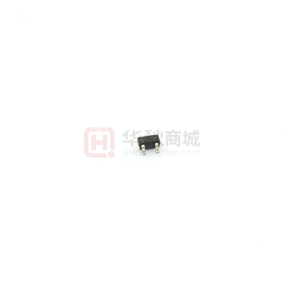
7. 封装信息:DMG1012T通常采用SOT-23封装,具有小尺寸和高可靠性。
DMG1012T 价格&库存

很抱歉,暂时无法提供与“DMG1012T”相匹配的价格&库存,您可以联系我们找货

免费人工找货