Datasheet for Telink
BLE + IEEE802.15.4 MultiStandard Wireless SoC
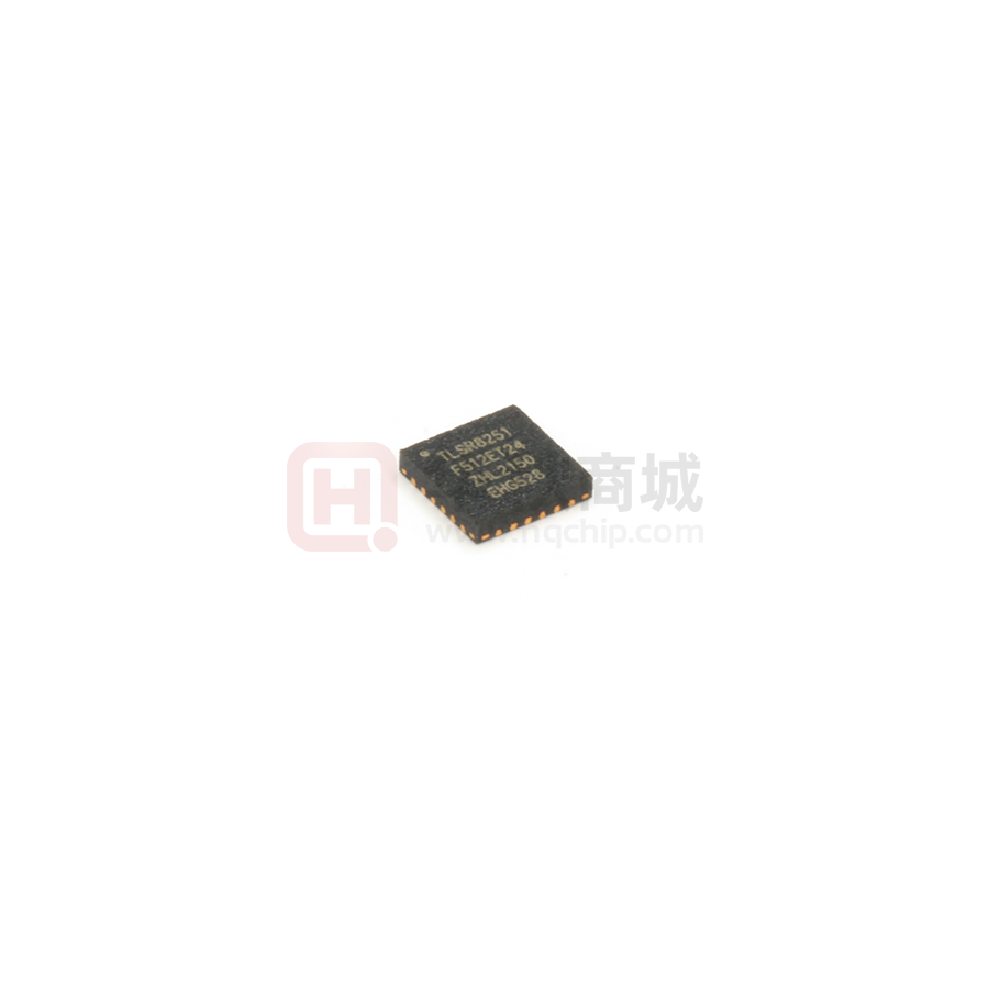
TLSR8251
DS-TLSR8251-E8
2020/3/13
Keyword:
BLE; BLE Mesh; 2.4GHz; Features; Package; Pin layout;
Memory; MCU; Working modes; Wakeup2016/1/29
sources; RF
Transceiver; Clock; Timers; Interrupt; Interface; PWM;
Audio; QDEC; ADC; PGA; Temperature sensor; Low power
comparator; AES; Electrical specification
Brief:
This datasheet is dedicated for Telink BLE + IEEE802.15.4
multi-standard SoC TLSR8251 (VID: 0x02). In this
datasheet, key features, working mode, main modules,
electrical specification and application of the TLSR8251
are introduced.
TELINK SEMICONDUCTOR
Ver 0.8.7
�Datasheet for Telink TLSR8251
Published by
Telink Semiconductor
Bldg 3, 1500 Zuchongzhi Rd,
Zhangjiang Hi-Tech Park, Shanghai, China
© Telink Semiconductor
All Right Reserved
Legal Disclaimer
This document is provided as-is. Telink Semiconductor reserves the right to make
improvements without further notice to this document or any products herein. This
document may contain technical inaccuracies or typographical errors. Telink
Semiconductor disclaims any and all liability for any errors, inaccuracies or
incompleteness contained herein.
Copyright (c) 2020 Telink Semiconductor (Shanghai) Ltd, Co.
Information:
For further information on the technology, product and business term, please contact
Telink Semiconductor Company (www.telink-semi.com).
For sales or technical support, please send email to the address of:
telinkcnsales@telink-semi.com
telinkcnsupport@telink-semi.com
DS-TLSR8251-E8
1
Ver 0.8.7
�Datasheet for Telink TLSR8251
Revision History
Version
Major Changes
Date
0.8.0
Preliminary release
2018/8
Author
YCQ, LY, JJW, SY, LWF,
LWT, SGJ, HZT, Cynthia
Updated section 1 Overview,
3
0.8.1
BLE/802.15.4/2.4GHz RF Transceiver,
7.3.4
I2C Master mode,
2018/11
SY, CJH, YCQ, HZF, Cynthia
16 Key Electrical Specifications,
17 Reference Design.
Updated section 2.4
Working modes,
2.5 Reset,
2.6.1 Power-On-Reset (POR) and
Brown-out detect,
4.2 System clock,
0.8.2
4.4 Register table,
2018/12
16.1 Absolute maximum ratings,
SY, SGJ, LY, JJW, LWT,
Cynthia
16.2 Recommended operating condition,
16.4 AC characteristics.
Added section 2.6.4
VBAT and VANT
power-supply mode and 16.7 Flash
characteristics.
Updated the sections below:
1.2.2
RF Features,
1.6 Pin layout,
2.1.3
E-Fuse,
5.1.1
Register table,
7.1.1.1
GPIO lookup table,
8.1 Register table,
9.1.2 DMIC input,
0.8.3
9.1.5
DFIFO,
9.2.5.2
Manual regulate in analog mode,
9.2.6
Register configuration,
9.3.1
Rate Matching,
9.3.3
Register configuration,
2019/6
XJ, YCQ, JJW, LX, TJB, SY,
HZT, Cynthia
10.4 QDEC reset,
10.7 Register table,
11 SAR ADC,
12 PGA,
13 Temperature Sensor,
15.4 Register table,
17 Reference Design.
DS-TLSR8251-E8
2
Ver 0.8.7
�Datasheet for Telink TLSR8251
Version
Major Changes
Date
Author
2019/8
CSJ, SY, JF
2019/11
SY, YH
2019/12
SY, HCL, YH
2020/3
SY, YJL
Updated the sections below:
related with hardware 7816 interface
0.8.4
Added Telink Mesh
1.2.1 General Features
1.2.2 RF Features
Added Section 1.2.6 BLE Mesh features
Update the section below:
0.8.5
Related with BLE spec description
1.1 Overview
1.1.1 General features
Update the section below:
1.2.2 RF feature
0.8.6
17 Reference Design
Remove
TLSR8251F512EU48
related
information
1. TLSR8251 now supports IEEE 802.15.4
standard, related changes including:
- Revised document title.
- Updated intro paragraphs in chapter 1
Overview, section 1.1
Block diagram,
section 1.2.2 RF Features, the heading of
chapter 3
BLE/802.15.4/2.4GHz RF
Transceiver, section 3.1
Block diagram,
and section 3.3.1 Packet format.
- Added section 1.2.8
Concurrent
mode
feature.
2. Content improvement, changes including:
0.8.7
- Updated intro paragraphs in chapter 1
Overview, section 1.1
Block diagram,
section 1.2.1 General features, section
1.2.2
RF Features, section 1.2.3
Features of power management
module, section 1.3
Typical applications,
section 2.1.1 SRAM/Register, section 2.1.2
Flash, section 2.2
Firmware
encryption, section 2.4 Working modes,
section 2.6.1 Power-On-Reset (POR) and
Brown-out detect, section 2.7.5 Register
table, section 3.2 Air interface data rate
and RF channel frequency, section 3.3.1
DS-TLSR8251-E8
3
Ver 0.8.7
�Datasheet for Telink TLSR8251
Version
Major Changes
Date
Packet format, section 4.4
table, section 5.1.1
Author
Register
Register table,
section 5.3 System Timer, section 6.2
Register configuration, section 7.1.3
Pull-up/Pull-down resistor, section 7.3.2
Register table, section 7.4.1 Register
table, section 7.5 UART, section 8.1
Register table, section 9.2.6 Register
configuration, section 9.3.3 Register
configuration, section 10.7 Register table,
section 11.4 Register table, section 12.4
Register table, chapter 13
Temperature Sensor, section 14.6
Register table, section 15.4
table, section 16.3
Register
DC characteristics,
section 16.4 AC characteristics, section
16.5
SPI characteristics, and section
16.6
I2C characteristics.
- Added section 1.2.6
BLE
section 16.8 Thermal
features,
characteristics,
section 16.9 ESD characteristics, section
16.10
DS-TLSR8251-E8
Storage condition.
4
Ver 0.8.7
�Datasheet for Telink TLSR8251
Table of Contents
1
2
Overview ..........................................................................................................................15
1.1
Block diagram............................................................................................................15
1.2
Key features ..............................................................................................................17
1.2.1
General features ................................................................................................17
1.2.2
RF Features ........................................................................................................18
1.2.3
Features of power management module..........................................................18
1.2.4
USB features ......................................................................................................19
1.2.5
Flash features ....................................................................................................19
1.2.6
BLE features .......................................................................................................19
1.2.7
BLE Mesh features .............................................................................................20
1.2.8
Concurrent mode feature .................................................................................20
1.3
Typical applications ...................................................................................................20
1.4
Ordering information ................................................................................................21
1.5
Package .....................................................................................................................22
1.6
Pin layout ..................................................................................................................25
1.6.1
Pin layout for TLSR8251F512ET48 .....................................................................25
1.6.2
Pin layout for TLSR8251F512ET32 .....................................................................28
1.6.3
Pin layout for TLSR8251F512ET24 .....................................................................31
1.6.4
Notes .................................................................................................................33
Memory and MCU ............................................................................................................35
2.1
Memory .....................................................................................................................35
2.1.1
SRAM/Register ..................................................................................................35
2.1.2
Flash...................................................................................................................36
2.1.3
E-Fuse ................................................................................................................37
2.2
Firmware encryption .................................................................................................37
2.3
MCU ..........................................................................................................................37
2.4
Working modes .........................................................................................................38
2.5
Reset .........................................................................................................................40
2.6
Power Management .................................................................................................41
2.6.1
Power-On-Reset (POR) and Brown-out detect..................................................41
2.6.2
Working mode switch........................................................................................44
2.6.3
LDO and DCDC ...................................................................................................45
2.6.4
VBAT and VANT power-supply mode ................................................................45
2.7
Wakeup sources ........................................................................................................46
2.7.1
Wakeup source - USB ........................................................................................46
DS-TLSR8251-E8
5
Ver 0.8.7
�Datasheet for Telink TLSR8251
3
4
2.7.2
Wakeup source – 32kHz timer ..........................................................................46
2.7.3
Wakeup source – low power comparator .........................................................46
2.7.4
Wakeup source – IO ..........................................................................................46
2.7.5
Register table.....................................................................................................47
BLE/802.15.4/2.4GHz RF Transceiver ...............................................................................49
3.1
Block diagram............................................................................................................49
3.2
Air interface data rate and RF channel frequency ....................................................50
3.3
Baseband ...................................................................................................................50
3.3.1
Packet format ....................................................................................................50
3.3.2
RSSI and frequency offset .................................................................................51
Clock .................................................................................................................................52
4.1
Clock sources.............................................................................................................52
4.2
System clock ..............................................................................................................53
4.3
Module clock .............................................................................................................53
4.3.1
System Timer clock ............................................................................................53
4.3.2
USB clock ...........................................................................................................53
4.3.3
I2S clock .............................................................................................................53
4.3.4
DMIC clock .........................................................................................................53
4.4
5
Timers ...............................................................................................................................56
5.1
6
7
Register table ............................................................................................................54
Timer0~Timer2 ..........................................................................................................56
5.1.1
Register table.....................................................................................................56
5.1.2
Mode0 (System Clock Mode) ............................................................................57
5.1.3
Mode1 (GPIO Trigger Mode) .............................................................................57
5.1.4
Mode2 (GPIO Pulse Width Mode) .....................................................................58
5.1.5
Mode3 (Tick Mode) ...........................................................................................59
5.1.6
Watchdog ..........................................................................................................60
5.2
32K LTIMER ...............................................................................................................60
5.3
System Timer ............................................................................................................60
Interrupt System ..............................................................................................................62
6.1
Interrupt structure ....................................................................................................62
6.2
Register configuration ...............................................................................................62
6.2.1
Enable/Mask interrupt sources .........................................................................63
6.2.2
Interrupt mode and priority ..............................................................................64
6.2.3
Interrupt source flag ..........................................................................................64
Interface ...........................................................................................................................65
7.1
GPIO ..........................................................................................................................65
DS-TLSR8251-E8
6
Ver 0.8.7
�Datasheet for Telink TLSR8251
7.1.1
7.1.1.1
GPIO lookup table ......................................................................................65
7.1.1.2
Multiplexed functions ................................................................................69
7.1.1.3
Drive strength ............................................................................................70
7.1.2
Connection relationship between GPIO and related modules .........................71
7.1.3
Pull-up/Pull-down resistor ................................................................................73
7.2
SWM and SWS...........................................................................................................75
7.3
I2C .............................................................................................................................75
7.3.1
Communication protocol ..................................................................................75
7.3.2
Register table.....................................................................................................76
7.3.3
I2C Slave mode ..................................................................................................76
7.3.3.1
DMA mode .................................................................................................77
7.3.3.2
Mapping mode...........................................................................................78
7.3.4
7.4
I2C Master mode ...............................................................................................78
7.3.4.1
I2C Master Write transfer ..........................................................................79
7.3.4.2
I2C Master Read transfer ...........................................................................79
7.3.5
8
Basic configuration ............................................................................................65
I2C and SPI Usage ..............................................................................................79
SPI..............................................................................................................................79
7.4.1
Register table.....................................................................................................80
7.4.2
SPI Master mode ...............................................................................................80
7.4.3
SPI Slave mode ..................................................................................................81
7.4.4
I2C and SPI Usage ..............................................................................................82
7.5
UART .........................................................................................................................82
7.6
USB ............................................................................................................................85
PWM .................................................................................................................................86
8.1
Register table ............................................................................................................86
8.2
Enable PWM ..............................................................................................................89
8.3
Set PWM clock ..........................................................................................................89
8.4
PWM waveform, polarity and output inversion .......................................................90
8.4.1
Waveform of signal frame .................................................................................90
8.4.2
Invert PWM output ...........................................................................................90
8.4.3
Polarity for signal frame ....................................................................................90
8.5
PWM mode ...............................................................................................................91
8.5.1
Select PWM mode .............................................................................................91
8.5.2
Continuous mode ..............................................................................................91
8.5.3
Counting mode ..................................................................................................92
8.5.4
IR mode .............................................................................................................92
DS-TLSR8251-E8
7
Ver 0.8.7
�Datasheet for Telink TLSR8251
8.5.5
IR FIFO mode .....................................................................................................93
8.5.6
IR DMA FIFO mode ............................................................................................94
8.6
9
PWM interrupt ..........................................................................................................98
Audio ................................................................................................................................99
9.1
Audio input path .......................................................................................................99
9.1.1
AMIC input.........................................................................................................99
9.1.2
DMIC input ......................................................................................................100
9.1.3
I2S input...........................................................................................................100
9.1.4
USB Host input ................................................................................................100
9.1.5
DFIFO ...............................................................................................................100
9.2
Audio input processing ...........................................................................................101
9.2.1
Decimation filter ..............................................................................................102
9.2.2
LPF ...................................................................................................................102
9.2.3
Down-sample...................................................................................................102
9.2.4
HPF ..................................................................................................................102
9.2.5
ALC ...................................................................................................................102
9.2.5.1
Auto regulate in analog mode .................................................................102
9.2.5.2
Manual regulate in analog mode .............................................................103
9.2.5.3
Auto regulate in digital mode ..................................................................103
9.2.5.4
Manual regulate in digital mode ..............................................................104
9.2.6
9.3
Register configuration .....................................................................................104
Audio output path ...................................................................................................108
9.3.1
Rate Matching .................................................................................................108
9.3.2
SDM .................................................................................................................109
9.3.3
Register configuration .....................................................................................110
10 Quadrature Decoder ......................................................................................................113
10.1
Input pin selection ..................................................................................................113
10.2
Common mode and double accuracy mode ...........................................................113
10.3
Read real time counting value ................................................................................115
10.4
QDEC reset ..............................................................................................................116
10.5
Other configuration ................................................................................................116
10.6
Timing sequence .....................................................................................................117
10.7
Register table ..........................................................................................................118
11 SAR ADC ..........................................................................................................................119
11.1
Power on/down ......................................................................................................119
11.2
ADC clock ................................................................................................................119
11.3
ADC control in auto mode.......................................................................................120
DS-TLSR8251-E8
8
Ver 0.8.7
�Datasheet for Telink TLSR8251
11.3.1
Set max state and enable channel ..................................................................120
11.3.2
“Set” state .......................................................................................................120
11.3.3
“Capture” state................................................................................................121
11.3.4
Usage cases .....................................................................................................122
11.4
11.3.4.1
Case 1: 3-channel sampling for stereo audio and Misc ...........................122
11.3.4.2
Case 2: 2-channel sampling for mono audio and Misc ............................122
11.3.4.3
Case 3: 2-channel sampling for stereo audio ...........................................122
11.3.4.4
Case 4: 1-channel sampling for mono audio ...........................................122
11.3.4.5
Case 5: 1-channel sampling for Misc .......................................................123
11.3.4.6
Case 6 with detailed register setting........................................................123
Register table ..........................................................................................................125
12 PGA .................................................................................................................................131
12.1
Power on/down ......................................................................................................132
12.2
Input channel ..........................................................................................................132
12.3
Adjust gain ..............................................................................................................132
12.4
Register table ..........................................................................................................133
13 Temperature Sensor.......................................................................................................134
14 Low Power Comparator .................................................................................................136
14.1
Power on/down ......................................................................................................136
14.2
Select input channel ................................................................................................136
14.3
Select mode and input channel for reference ........................................................137
14.4
Select scaling coefficient .........................................................................................137
14.5
Low power comparator output...............................................................................137
14.6
Register table ..........................................................................................................137
15 AES ..................................................................................................................................139
15.1
RISC mode ...............................................................................................................139
15.2
DMA mode ..............................................................................................................139
15.3
AES-CCM..................................................................................................................139
15.4
Register table ..........................................................................................................140
16 Key Electrical Specifications ...........................................................................................141
16.1
Absolute maximum ratings .....................................................................................141
16.2
Recommended operating condition .......................................................................141
16.3
DC characteristics ....................................................................................................142
16.4
AC characteristics ....................................................................................................142
16.5
SPI characteristics ...................................................................................................149
16.6
I2C characteristics ...................................................................................................150
16.7
Flash characteristics ................................................................................................151
DS-TLSR8251-E8
9
Ver 0.8.7
�Datasheet for Telink TLSR8251
16.8
Thermal characteristics ...........................................................................................152
16.9
ESD characteristics ..................................................................................................152
16.10 Storage condition ....................................................................................................153
17 Reference Design ...........................................................................................................154
17.1
Application example for TLSR8251F512ET48 .........................................................154
17.1.1
Schematic ........................................................................................................154
17.1.2
BOM (Bill of Material)......................................................................................155
17.2
Application example for TLSR8251F512ET32 .........................................................156
17.2.1
Schematic ........................................................................................................156
17.2.2
BOM (Bill of Material)......................................................................................157
17.3
Application example for TLSR8251F512ET24 .........................................................158
17.3.1
Schematic ........................................................................................................158
17.3.2
BOM (Bill of Material)......................................................................................159
DS-TLSR8251-E8
10
Ver 0.8.7
�Datasheet for Telink TLSR8251
List of Figures
Figure 1- 1
Block diagram of the system ....................................................................... 16
Figure 1- 2
Package dimension for TLSR8251F512ET48 (Unit: mm) ............................. 22
Figure 1- 3
Package dimension for TLSR8251F512ET32 (Unit: mm) ............................. 23
Figure 1- 4
Package dimension for TLSR8251F512ET24 (Unit: mm) ............................. 24
Figure 1- 5
Pin assignment for TLSR8251F512ET48 ...................................................... 25
Figure 1- 6
Pin assignment for TLSR8251F512ET32 ...................................................... 28
Figure 1- 7
Pin assignment for TLSR8251F512ET24 ...................................................... 31
Figure 2- 1
Physical memory map ................................................................................. 35
Figure 2- 2
Register space ............................................................................................. 36
Figure 2- 3
Control logic for power up/down ............................................................... 41
Figure 2- 4
Initial Power-up sequence .......................................................................... 42
Figure 2- 5
Power-down sequence ............................................................................... 43
Figure 2- 6
Wakeup sources .......................................................................................... 46
Figure 3- 1
Block diagram of RF transceiver.................................................................. 49
Figure 4- 1
Block diagram of clock ................................................................................ 52
Figure 7- 1
Logic relationship between GPIO and related modules ............................. 71
Figure 7- 2
I2C timing chart........................................................................................... 75
Figure 7- 3
Byte consisted of slave address and R/W flag bit ....................................... 77
Figure 7- 4
Read format in DMA mode ......................................................................... 77
Figure 7- 5
Write format in DMA mode ........................................................................ 77
Figure 7- 6
Read format in Mapping mode ................................................................... 78
Figure 7- 7
Write format in Mapping mode .................................................................. 78
Figure 7- 8
SPI write/read command format ................................................................ 82
Figure 7- 9
UART communication ................................................................................. 83
Figure 8- 1
A signal frame ............................................................................................. 90
Figure 8- 2
PWM output waveform chart ..................................................................... 91
Figure 8- 3
Continuous mode........................................................................................ 91
Figure 8- 4
Counting mode (n=0) .................................................................................. 92
Figure 8- 5
IR mode (n=0) ............................................................................................. 93
Figure 8- 6
IR format examples ..................................................................................... 94
Figure 9- 1
Audio input path ......................................................................................... 99
Figure 9- 2
Audio input processing ............................................................................. 101
Figure 9- 3
Audio output path .................................................................................... 108
Figure 9- 4
Linear interpolation .................................................................................. 109
Figure 9- 5
Delay interpolation ................................................................................... 109
DS-TLSR8251-E8
11
Ver 0.8.7
�Datasheet for Telink TLSR8251
Figure 9- 6
Block diagram of SDM ............................................................................... 109
Figure 10- 1 Common mode .................................................................................. 114
Figure 10- 2 Double accuracy mode ....................................................................... 115
Figure 10- 3 Read real time counting value ............................................................. 116
Figure 10- 4 Shuttle mode ..................................................................................... 116
Figure 10- 5 Timing sequence chart ....................................................................... 117
Figure 11- 1 Block diagram of ADC ......................................................................... 119
Figure 12- 1 Block diagram of PGA ......................................................................... 131
Figure 13- 1 Block diagram of temperature sensor .................................................. 134
Figure 14- 1 Block diagram of low power comparator.............................................. 136
Figure 16- 1 SPI Timing Diagram, Master Mode....................................................... 149
Figure 16- 2 SPI Timing Diagram, Slave Mode ......................................................... 149
Figure 16- 3 I2C Timing Diagram ............................................................................ 150
Figure 17- 1 Schematic for TLSR8251F512ET48 ....................................................... 154
Figure 17- 2 Schematic for TLSR8251F512ET32 ....................................................... 156
Figure 17- 3 Schematic for TLSR8251F512ET24 ....................................................... 158
DS-TLSR8251-E8
12
Ver 0.8.7
�Datasheet for Telink TLSR8251
List of Tables
Table 1- 1
Ordering information of the TLSR8251* ..................................................... 21
Table 1- 2
Pin functions for TLSR8251F512ET48 ......................................................... 26
Table 1- 3
Pin functions for TLSR8251F512ET32 ......................................................... 29
Table 1- 4
Pin functions for TLSR8251F512ET24 ......................................................... 31
Table 2- 1
E-Fuse information ...................................................................................... 37
Table 2- 2
Working modes ........................................................................................... 38
Table 2- 3
Retention analog registers in deep sleep .................................................... 39
Table 2- 4
Register configuration for software reset ................................................... 40
Table 2- 5
Analog register to control delay counters ................................................... 41
Table 2- 6
Characteristics of Initial Power-up/ Power-down sequence ...................... 43
Table 2- 7
3.3V analog registers for module power up/down control ........................ 44
Table 2- 8
Analog registers for Wakeup ....................................................................... 47
Table 2- 9
Digital register for Wakeup ......................................................................... 48
Table 3- 1
External RF transceiver control example .................................................... 49
Table 3- 2
Packet Format in standard 1Mbps BLE mode ............................................. 50
Table 3- 3
Packet format in standard 2Mbps BLE mode .............................................. 51
Table 3- 4
Packet Format In Standard 500kbps/125kbps BLE Mode ........................... 51
Table 3- 5
Packet format in 802.15.4 Mode ................................................................ 51
Table 3- 6
Packet format in Proprietary mode ............................................................ 51
Table 4- 1
Register table related to clock .................................................................... 54
Table 5- 1
Register configuration for Timer0~Timer2 ................................................. 56
Table 5- 2
Register table for System Timer .................................................................. 60
Table 6- 1
Register table for Interrupt system ............................................................. 62
Table 7- 1
GPIO lookup table 1 .................................................................................... 65
Table 7- 2
Select multiplexed SPI/I2C .......................................................................... 70
Table 7- 3
GPIO lookup table2 ..................................................................................... 72
Table 7- 4
Analog registers for pull-up/pull-down resistor control ............................. 73
Table 7- 5
Register configuration for I2C ..................................................................... 76
Table 7- 6
Register configuration for SPI ..................................................................... 80
Table 7- 7
SPI Master mode ......................................................................................... 80
Table 7- 8
SPI Slave mode ............................................................................................ 81
Table 7- 9
Register configuration for UART ................................................................. 83
Table 8- 1
Register table for PWM ............................................................................... 86
Table 9- 1
Audio data flow direction ........................................................................... 99
Table 9- 2
Register configuration related to audio input processing......................... 104
DS-TLSR8251-E8
13
Ver 0.8.7
�Datasheet for Telink TLSR8251
Table 9- 3
Register configuration related to audio output path ................................ 111
Table 10- 1
Input pin selection ............................................................................. 113
Table 10- 2
Timing ............................................................................................... 117
Table 10- 3
Register table for QDEC ...................................................................... 118
Table 11- 1
Overall register setting........................................................................ 123
Table 11- 2
Register setting for L/R/M channel ...................................................... 124
Table 11- 3
Register table related to SAR ADC ........................................................ 125
Table 12- 1
Analog register table related to PGA .................................................... 133
Table 13- 1
Analog register for temperature sensor ............................................... 134
Table 14- 1
Analog register table related to low power comparator ........................ 137
Table 15- 1
Register table related to AES ............................................................... 140
Table 16- 1
Absolute Maximum Ratings ................................................................ 141
Table 16- 2
Recommended operation condition .................................................... 141
Table 16- 3
DC characteristics ............................................................................... 142
Table 16- 4
AC Characteristics (VDD=3.3V, Ta=25℃) .............................................. 142
Table 16- 5
SPI characteristics............................................................................... 149
Table 16- 6
I2C characteristics .............................................................................. 150
Table 16- 7
Flash memory characteristics .............................................................. 151
Table 16- 8
Thermal characteristics ....................................................................... 152
Table 16- 9
Thermal characteristics ....................................................................... 152
Table 16- 10 HBM/CDM Results.............................................................................. 152
Table 16- 11 LU Test Result..................................................................................... 153
Table 17- 1
BOM table for TLSR8251F512ET48 ...................................................... 155
Table 17- 2
BOM table for TLSR8251F512ET32 ...................................................... 157
Table 17- 3
BOM table for TLSR8251F512ET24 ...................................................... 159
DS-TLSR8251-E8
14
Ver 0.8.7
�Datasheet for Telink TLSR8251
1
Overview
The TLSR8251 is Telink-developed Bluetooth LE + IEEE802.15.4 multi-standard wireless SoC
solution with internal Flash and audio support. It’s completely RoHS-compliant and 100% lead (Pb)free.
The TLSR8251 combines the radio frequency (RF), digital processing, protocols stack software
and profiles for Bluetooth Low Energy (up to Bluetooth 5.0), BLE Mesh and 2.4GHz proprietary
standard into a single SoC. The TLSR8251’s embedded 512kB FLASH enables dynamic stack and
profile configuration, and the final end product functionality is configurable via software, providing
ultimate flexibility. The TLSR8251 also has hardware OTA upgrades support and multiple boot
switching, allowing convenient product feature roll outs and upgrades.
The TLSR8251 supports concurrent multi-standards. For some use cases, the TLSR8251 can
“concurrently” run two standards, for example, stacks such as BLE and 802.15.4 can run concurrently
with one application state but dual radio communication channels for interacting with different
devices. The end product working in this mode can maintain active Bluetooth Smart connections to
smart phones or other BLE devices while control and communicate with 802.15.4 or other 2.4GHz
devices at the same time. In this case, it’s compatible with Bluetooth standard, supports BLE
specification up to Bluetooth 5.0, allows easy connectivity with Bluetooth Smart Ready mobile
phones, tablets, laptops, which supports BLE slave and master mode operation, including broadcast,
encryption, connection updates, and channel map updates. At the same time, it also supports IEEE
802.15.4 standard, and is perfect for creating interoperable solution for use within the home. This
feature enables products to bridge the smartphone and home automation world with a single chip
and no requirement for an external hub.
The TLSR8251 integrates hardware acceleration to support the complicated security operations
required by Bluetooth, up to and including the 5.0 standard, without the requirement for an external
DSP, thereby significantly reducing the product eBOM.
The TLSR8251 supports single or dual analog microphones or digital microphone, and stereo
audio output with enhanced voice performance for voice search and other such applications. The
TLSR8251 also includes a full range of on-chip peripherals for interfacing with external components
such as LEDs, sensors, touch controllers, keyboards, and motors. This makes it an ideal single-chip
solution for IoT (Internet of Things) and HID (Human Interface Devices) application such as wearable
devices, smart lighting, smart home devices, advanced remote controls, and wireless toys.
1.1 Block diagram
The TLSR8251 is designed to offer high integration, ultra-low power application capabilities.
The system’s block diagram is as shown in Figure 1-1.
DS-TLSR8251-E8
15
Ver 0.8.7
�Datasheet for Telink TLSR8251
POWER MANAGEMENT
RESET
POWER-ON
RESET
BROWN OUT
LDO & DCDC
POWER
Management
Controller
CLOCK
MEMORY
24MHz Crystal
Oscillator
24MHz RC
Oscillator
32kB SRAM
32.768kHz Crystal
Oscillator*
32kHz RC
Oscillator
512kB FLASH
BLE/802.15.4/
2.4GHz Radio
I2C
SPI
Timer0/1/2
Watchdog
UART
1 Quadrature
Decoder
GPIO
USB
RISC 32bit MCU
Swire
PWM
I2S
2 x SDM
DMIC
14bit ADC
AMIC
PGA
Figure 1- 1
Block diagram of the system
*Notes:
1) Modules marked with different colors belong to different power domains. Power state of each
power domain can be controlled independent of other power domains, for example, the audio
module (including I2S, DMIC, AMIC) can be independently powered on or powered down
irrespective of other modules such as power management module, clock, and etc.
2)
The BLE/802.15.4/2.4GHz Radio, USB and Audio (I2S, DMIC, AMIC) are powered down by
default.
3)
The power management module and clock should be always powered on, even in deep sleep.
4)
In deep sleep, except for the power management and clock, all other modules should be
powered down.
The TLSR8251 integrates a power-balanced 32-bit MCU, BLE/802.15.4/2.4GHz Radio, 32kB
SRAM, 512kB internal Flash, 14bit ADC with PGA, analog and digital microphone input, stereo audio
output, 6-channel PWM (1-channel IR/IR FIFO/IR DMA FIFO), one quadrature decoder (QDEC),
abundant and flexible GPIO interfaces, and nearly all the peripherals needed for IoT (Internet of
Things) and HID (Human Interface Devices) application development (e.g. Bluetooth Low Energy and
IEEE 802.15.4). The TLSR8251 also includes multi-stage power management design allowing ultralow power operation and making it the ideal candidate for wearable and power-constraint
applications.
With the high integration level of TLSR8251, few external components are needed to satisfy
customers’ ultra-low cost requirements.
DS-TLSR8251-E8
16
Ver 0.8.7
�Datasheet for Telink TLSR8251
1.2 Key features
1.2.1
General features
General features are as follows:
1) 4-byte Chip UID (Unique ID).
2) Embedded 32-bit proprietary microcontroller.
Better power-balanced performance than ARM M0
Instruction cache controller
Maximum running speed up to 48MHz
3) Program memory: internal 512kB Flash.
4) Data memory: 32kB on-chip SRAM, including up to 32kB SRAM with retention in deep
sleep
5) RTC and other timers:
Clock source of 24MHz&32.768kHz Crystal and 32kHz/24MHz embedded RC
oscillator, among which, the external 24MHz is to verify internal 32K clock, the
internal 32KHz is for low precision application, external 32.768 is for high precision
application
Three general 32-bit timers with four selectable modes in active mode
Watchdog timer
A low-frequency 32kHz timer available in low power mode
6) A rich set of I/Os:
Up to 32/17/10 GPIOs depending on package option. All digital IOs can be used as
GPIOS.
DMIC (Digital Mic).
AMIC (Analog Mic).
I2S.
Stereo Audio output.
SPI.
I2C.
UART with hardware flow control and 7816 protocol support.
USB.
Swire debug Interface.
7) Up to 6 channels of differential PWM:
PWM1~PWM5: 5-channel normal PWM output.
PWM0: 1 channel with IR/IR FIFO/IR DMA FIFO mode for IR generation.
8) Sensor:
14bit 10-channel (only GPIO input) SAR ADC, with 4-channel differential input PGA,
DS-TLSR8251-E8
17
Ver 0.8.7
�Datasheet for Telink TLSR8251
effective bits: 10.5bits
Temperature sensor
9) One quadrature decoder.
10) Embedded hardware AES block cipher with 128 bit keys and software AES-CCM.
11) Embedded hardware acceleration for Elliptical curve cryptography (ECC) supports
Bluetooth standard up to and including BLE 5.0.
12) Embedded low power comparator.
13) Operating temperature: -40℃~+85℃
14) Supports BLE, BLE Mesh and 2.4GHz proprietary technologies into a single SoC without
the requirement for an external DSP.
1.2.2
RF Features
RF features include:
1) BLE/802.15.4/2.4GHz RF transceiver embedded, working in worldwide 2.4GHz ISM band.
2) Bluetooth 5.0 Compliant, 1Mbps, 2Mbps, Long Range 125kbps and 500kbps mode.
3) IEEE802.15.4 compliant, 250kbps.
4) 2.4GHz proprietary 1Mbps/2Mbps/250kbps/500kbps mode with Adaptive Frequency
Hopping feature support.
5) ANT mode
6) Rx Sensitivity: -96dBm@BLE 1Mbps mode, -99.5dBm@ IEEE802.15.4 250kbps mode, 93dBm @ BLE 2Mbps mode, -99dBm @ BLE 500kbps mode, -101dBm @ BLE 125kbps
mode.
7) Tx output power: up to +10dBm.
8) Single-pin antenna interface.
9) RSSI monitoring with +/-1dB resolution.
10) Auto acknowledgement, retransmission and flow control.
11) Support single-antenna AOA/TX BLE location features.
1.2.3
Features of power management module
Features of power management module include:
1) Embedded LDO and DCDC.
2) Battery monitor: Supports low battery detection.
3) Power supply: 1.8V~3.6V.
4) Multiple stage power management to minimize power consumption.
5) Low power consumption:
Whole Chip RX mode: 5.3mA
DS-TLSR8251-E8
18
Ver 0.8.7
�Datasheet for Telink TLSR8251
1.2.4
Whole Chip TX mode: 4.8mA @ 0dBm with DCDC
Deep sleep with external wakeup (without SRAM retention): 0.4µA
Deep sleep with SRAM retention: 1µA (with 8kB SRAM retention), 1.2µA (with 16kB
SRAM retention), 1.4µA (with 32kB SRAM retention)
Deep sleep with external wakeup, with 32K RC oscillator on (without SRAM retention):
0.9µA
Deep sleep with SRAM retention, with 32K RC oscillator on: 1.5µA (with 8kB SRAM
retention), 1.7µA (with 16kB SRAM retention), 1.9µA (with 32kB SRAM retention)
USB features
USB features include:
1) Compatible with USB2.0 Full speed mode.
2) Supports 9 endpoints including control endpoint 0 and 8 configurable data endpoints.
3) Independent power domain.
4) Supports ISP (In-System Programming) via USB port.
1.2.5
Flash features
The TLSR8251 embeds Flash with features below:
1) Total 512kB (4Mbits).
2) Flexible architecture: 4kB per Sector, 64kB/32kB per block.
3) Up to 256 Bytes per programmable page.
4) Write protect all or portions of memory.
5) Sector erase (4kB).
6) Block erase (32kB/64kB).
7) Cycle Endurance: 100,000 program/erases.
8) Data Retention: typical 20-year retention.
9) Multi firmware encryption methods for anti-cloning protection.
1.2.6
BLE features
1) Bluetooth 5.0 support
2) Long range support with 125Kbps and 500Kbps data rate
3) Telink proprietary Mesh support
4) Support single-antenna AOA/TX BLE location features
5) Telink extended profile with audio support for voice command based searches
DS-TLSR8251-E8
19
Ver 0.8.7
�Datasheet for Telink TLSR8251
1.2.7
BLE Mesh features
Telink Proprietary BLE Mesh features include:
1) Support flexible mesh control, e.g. N-to-1 and N-to-M;
2) Supports switch control for over 200 nodes without delay;
3) Supports real time status update for over 200 nodes;
4) Secure and safe control and scalable identification within network;
5) 8/16 groups can be controlled at the same time;
6) 128/256 nodes within mesh network;
7) Configurable to more or fewer hops (e.g. 4 hops) within mesh network, single hop delay
less than 15ms;
8) Flexible RF channel usage with both BLE advertising channels and data channels for good
anti-interference performance.
1.2.8
Concurrent mode feature
In concurrent mode, the chip supports multiple standard working concurrently.
Typical combination is Bluetooth LE + 802.15.4 based standard: BLE and 802.15.4 based stacks
can run concurrently with one application state based on time division technology, e.g. BLE stack
will run alternately during the divided time slots.
1.3 Typical applications
The TLSR8251 can be applied to IoT (Internet of Things) and HID (Human Interface Devices)
applications, such as BLE smart devices, BLE mesh devices, and 2.4GHz IEEE 802.15.4 remote control
/set-top box.
Its typical applications include, but are not limited to the following:
Smartphone and tablet accessories
RF Remote Control
Sports and fitness tracking
Wearable devices
Wireless toys
Smart Lighting, Smart Home devices
Building Automation
Smart Grid
Intelligent Logistics/Transportation/City
Consumer Electronics
Industrial Control
Health Care
DS-TLSR8251-E8
20
Ver 0.8.7
�Datasheet for Telink TLSR8251
1.4 Ordering information
Table 1- 1
Product Series
Package Type
TLSR8251F512
48-pin TQFN
7x7x0.75mm
32-pin TQFN
5x5x0.75mm
24-pin TQFN
4×4x0.75mm
Ordering information of the TLSR8251*1
Temperature
Range
-40℃~+85℃
-40℃~+85℃
-40℃~+85℃
Product Part
No.
TLSR8251F512
ET48
TLSR8251F512
ET32
TLSR8251F512
ET24
Packing
Method
*2
Minimum Order
Quantity
TR
3000
TR
3000
TR
3000
1
MSL (Moisture Sensitivity Level): The 8251 series is applicable to MSL3 (Based on JEDEC Standard J-STD-020).
After the packing opened, the product shall be stored at PB~PB, 0x5e2[7:0] --> PC~PC,
0x5e3[7:0] --> PD~PD.
(3) Timer/Counter counting or control signal:
Configure “Polarity”. In Timer Mode 1, it determines GPIO edge when Timer Tick counting
increases. In Timer Mode 2, it determines GPIO edge when Timer Tick starts counting.
Then set “m0/m1/m2” to specify the GPIO which generates counting signal (Mode 1)/control
signal (Mode 2) for Timer0/Timer1/Timer2.
User can read addresses 0x5e8~0x5eb/0x5f0~0x5f3/0x5f8~0x5fb to see which GPIO asserts
counting signal (in Mode 1) or control signal (in Mode 2) for Timer0/Timer1/Timer2. Note:
Timer0: 0x5e8[7:0] --> PA~PA, 0x5e9[7:0] --> PB~PB, 0x5ea[7:0] -->
PC~PC, 0x5eb[7:0] --> PD~PD; Timer1: 0x5f0[7:0] --> PA~PA, 0x5f1[7:0] -> PB~PB, 0x5f2[7:0] --> PC~PC, 0x5f3[7:0] --> PD~PD; Timer2: 0x5f8[7:0]
--> PA~PA, 0x5f9[7:0] --> PB~PB, 0x5fa[7:0] --> PC~PC, 0x5fb[7:0] -->
PD~PD.
(4) GPIO2RISC IRQ signal:
Select GPIO2RISC interrupt trigger edge (positive edge or negative edge) via configuring
“Polarity”, and set corresponding GPIO enabling bit “m0”/“m1”.
Enable GPIO2RISC[0]/GPIO2RISC[1] interrupt, i.e. “gpio2risc[0]” (address 0x642[5]) /
“gpio2risc[1]”(address 0x642[6]).
Pin
Input
(R)
PA
PA
PA
PA
PA
PA
PA
PA
PB
PB
PB
PB
PB
PB
0x580[0]
0x580[1]
0x580[2]
0x580[3]
0x580[4]
0x580[5]
0x580[6]
0x580[7]
0x588[0]
0x588[1]
0x588[2]
0x588[3]
0x588[4]
0x588[5]
DS-TLSR8251-E8
Table 7- 3 GPIO lookup table2
Polarity
1: active low
Irq
m0
0: active high
0x584[0]
0x587[0] 0x5b8[0]
0x584[1]
0x587[1] 0x5b8[1]
0x584[2]
0x587[2] 0x5b8[2]
0x584[3]
0x587[3] 0x5b8[3]
0x584[4]
0x587[4] 0x5b8[4]
0x584[5]
0x587[5] 0x5b8[5]
0x584[6]
0x587[6] 0x5b8[6]
0x584[7]
0x587[7] 0x5b8[7]
0x58c[0]
0x58f[0] 0x5b9[0]
0x58c[1]
0x58f[1] 0x5b9[1]
0x58c[2]
0x58f[2] 0x5b9[2]
0x58c[3]
0x58f[3] 0x5b9[3]
0x58c[4]
0x58f[4] 0x5b9[4]
0x58c[5]
0x58f[5] 0x5b9[5]
72
m1
m2
0x5c0[0]
0x5c0[1]
0x5c0[2]
0x5c0[3]
0x5c0[4]
0x5c0[5]
0x5c0[6]
0x5c0[7]
0x5c1[0]
0x5c1[1]
0x5c1[2]
0x5c1[3]
0x5c1[4]
0x5c1[5]
0x5c8[0]
0x5c8[1]
0x5c8[2]
0x5c8[3]
0x5c8[4]
0x5c8[5]
0x5c8[6]
0x5c8[7]
0x5c9[0]
0x5c9[1]
0x5c9[2]
0x5c9[3]
0x5c9[4]
0x5c9[5]
Ver 0.8.7
�Datasheet for Telink TLSR8251
Pin
Input
(R)
PB
PB
PC
PC
PC
PC
PC
PC
PC
PC
PD
PD
PD
PD
PD
PD
PD
PD
0x588[6]
0x588[7]
0x590[0]
0x590[1]
0x590[2]
0x590[3]
0x590[4]
0x590[5]
0x590[6]
0x590[7]
0x598[0]
0x598[1]
0x598[2]
0x598[3]
0x598[4]
0x598[5]
0x598[6]
0x598[7]
7.1.3
Polarity
1: active low
0: active high
0x58c[6]
0x58c[7]
0x594[0]
0x594[1]
0x594[2]
0x594[3]
0x594[4]
0x594[5]
0x594[6]
0x594[7]
0x59c[0]
0x59c[1]
0x59c[2]
0x59c[3]
0x59c[4]
0x59c[5]
0x59c[6]
0x59c[7]
Irq
m0
m1
m2
0x58f[6]
0x58f[7]
0x597[0]
0x597[1]
0x597[2]
0x597[3]
0x597[4]
0x597[5]
0x597[6]
0x597[7]
0x59f[0]
0x59f[1]
0x59f[2]
0x59f[3]
0x59f[4]
0x59f[5]
0x59f[6]
0x59f[7]
0x5b9[6]
0x5b9[7]
0x5ba[0]
0x5ba[1]
0x5ba[2]
0x5ba[3]
0x5ba[4]
0x5ba[5]
0x5ba[6]
0x5ba[7]
0x5bb[0]
0x5bb[1]
0x5bb[2]
0x5bb[3]
0x5bb[4]
0x5bb[5]
0x5bb[6]
0x5bb[7]
0x5c1[6]
0x5c1[7]
0x5c2[0]
0x5c2[1]
0x5c2[2]
0x5c2[3]
0x5c2[4]
0x5c2[5]
0x5c2[6]
0x5c2[7]
0x5c3[0]
0x5c3[1]
0x5c3[2]
0x5c3[3]
0x5c3[4]
0x5c3[5]
0x5c3[6]
0x5c3[7]
0x5c9[6]
0x5c9[7]
0x5ca[0]
0x5ca[1]
0x5ca[2]
0x5ca[3]
0x5ca[4]
0x5ca[5]
0x5ca[6]
0x5ca[7]
0x5cb[0]
0x5cb[1]
0x5cb[2]
0x5cb[3]
0x5cb[4]
0x5cb[5]
0x5cb[6]
0x5cb[7]
Pull-up/Pull-down resistor
All GPIOs (including PA~PD) support configurable pull-up resistor of rank x1 and x100
or pull-down resistor of rank x10 which are all disabled by default. Analog registers
afe_0x0e~afe_0x15 serve to control the pull-up/pull-down resistor for each GPIO.
The DP pin also supports 1.5kΩ pull-up resistor for USB use. The 1.5kΩ pull up resistor is
disabled by default and can be enabled by setting analog register afe_0x0b as 1b’1. For the
DP/PA pin, user can only enable either 1.5kΩ pull-up resistor or pull-up resistor of rank x1/x100
/ pull-down resistor of rank x10 at the same time. Please refer to Table 7- 4 for details.
Take the PA for example: Setting analog register afe_0x0e to 2b’01/2b’11/2b’10 is to
respectively enable pull-up resistor of rank x100/pull-up resistor of rank x1/pull-down resistor of
rank x10 for PA; Clearing the two bits (default value) disables pull-up and pull-down resistor for
PA.
Table 7- 4
Address
afe_0x0b
Rank
x1
x10
x100
DS-TLSR8251-E8
Analog registers for pull-up/pull-down resistor control
Mnemonic
Default
Description
1.5k (Typ.) pull-up resistor for USB DP PAD
0: disable
1: enable
Typical value (depend on actual application)
18kohm
160kohm
1Mohm
dp_pullup_res_3v
0x0
73
Ver 0.8.7
�Datasheet for Telink TLSR8251
Address
Mnemonic
Default
afe_0x0e
a_sel
0x00000000
afe_0x0f
a_sel
0x00000000
afe_0x10
b_sel
0x00000000
afe_0x11
b_sel
0x00000000
afe_0x12
c_sel
0x00000000
afe_0x13
c_sel
0x00000000
afe_0x14
d_sel
0x00000000
DS-TLSR8251-E8
74
Description
PA pull up and down select:
: PA
: PA
: PA
: PA
00: Null
01: x100 pull up
10: x10 pull down
11: x1 pull up
PA pull up and down select:
: PA
: PA
: PA
: PA
00: Null
01: x100 pull up
10: x10 pull down
11: x1 pull up
PB pull up and down select:
00: Null
01: x100 pull up
10: x10 pull down
11: x1 pull up
PB pull up and down select:
00: Null
01: x100 pull up
10: x10 pull down
11: x1 pull up
PC pull up and down select:
00: Null
01: x100 pull up
10: x10 pull down
11: x1 pull up
PC pull up and down select:
00: Null
01: x100 pull up
10: x10 pull down
11: x1 pull up
PD pull up and down select:
00: Null
01: x100 pull up
10: x10 pull down
11: x1 pull up
Ver 0.8.7
�Datasheet for Telink TLSR8251
Address
afe_0x15
Mnemonic
d_sel
Default
00000000
Description
PD pull up and down select:
00: Null
01: x100 pull up
10: x10 pull down
11: x1 pull up
7.2 SWM and SWS
The TLSR8251 supports Single Wire interface. SWM (Single Wire Master) and SWS (Single Wire
Slave) represent the master and slave device of the single wire communication system developed
by Telink. The maximum data rate can be up to 2Mbps.
7.3 I2C
The TLSR8251 embeds I2C hardware module, which could act as Master mode or Slave mode.
I2C is a popular inter-IC interface requiring only 2 bus lines, a serial data line (SDA) and a serial clock
line (SCL).
7.3.1
Communication protocol
Telink I2C module supports standard mode (100kbps) and Fast-mode (400kbps) with restriction
that system clock must be by at least 10x of data rate.
Two wires, SDA and SCL (SCK) carry information between Master device and Slave device
connected to the bus. Each device is recognized by unique address (ID). Master device is the device
which initiates a data transfer on the bus and generates the clock signals to permit that transfer.
Slave device is the device addressed by a Master.
Both SDA and SCL are bidirectional lines connected to a positive supply voltage via a pull-up
resister. It’s recommended to use external 3.3kohm pull-up resistor. For standard mode, the internal
pull-up resistor of rank x1 can be used instead of the external 3.3kohm pull-up.
When the bus is free, both lines are HIGH. It’s noted that data in SDA line must keep stable
when clock signal in SCL line is at high level, and level state in SDA line is only allowed to change
when clock signal in SCL line is at low level.
Figure 7- 2
DS-TLSR8251-E8
I2C timing chart
75
Ver 0.8.7
�Datasheet for Telink TLSR8251
7.3.2
Register table
Table 7- 5
Register configuration for I2C
Address
R/W
Description
0x00
0x01
RW
RW
0x02
RW
0x03
RW
0x04
0x05
0x06
RW
RW
RW
0x07
RW
0xe0
0xe1
0xe2
0xe3
R
RW
RW
RW
0xe4
RW
I2C master clock speed
[7:1] I2C ID
[0]: master busy
[1]: master packet busy
[2]: master received status
0 for ACK; 1 for NAK
[0]: address auto increase enable
[1]: I2C master enable
[2]: enable Mapping Mode
[3]: r_clk_stretch_en, suspend transmission by pulling
SCL down to low level, and continue transmission after
SCL is released to high level
[7:0] data buffer in master mode
[7:0] Data buffer in master mode
[7:0] Data buffer for Read or Write in master mode
[0]: launch ID cycle
[1]: launch address cycle
(send I2CAD data)
[2]: launch data write cycle
[3]: launch data read cycle
For Master Write: 0: I2CAD&I2CDW,
1: I2CAD&I2CDW&I2CDR)
To write 3 bytes: bit[3]=1;
To write 2 bytes: bit[3]=0.
For Master Read: always 1.
[4]: launch start cycle
[5]: launch stop cycle
[6]: enable read ID
[7]: enable ACK in read command
[6:0] I2C read address
Low byte of Mapping mode buffer address
Middle byte of Mapping mode buffer address
High byte of Mapping mode buffer address
[0]: host_cmd_irq_o,
I2C host operation has happened. Write 1 to clear.
[1]: host_rd_tag_o,
I2C host operation has happened and is read operation.
Write 1 to clear.
7.3.3
Default
Value
0x1f
0x5c
0x00
0x01
0x5a
0xf1
0x00
0x00
0x00
0x80
0xd7
0x00
0x00
I2C Slave mode
I2C module of the TLSR8251 acts as Slave mode by default. I2C slave address can be configured
via register I2C_ID (address 0x01) [7:1].
DS-TLSR8251-E8
76
Ver 0.8.7
�Datasheet for Telink TLSR8251
Figure 7- 3 Byte consisted of slave address and R/W flag bit
I2C slave mode supports two sub modes including Direct Memory Access (DMA) mode and
Mapping mode, which is selectable via address 0x03[2].
In I2C Slave mode, Master could initiate transaction anytime. I2C slave module will reply with
ACK automatically. To monitor the start of I2C transaction, user could set interrupt from GPIO for
SCA or SCL.
7.3.3.1
DMA mode
In DMA mode, other devices (Master) could access (read/write) designated address in Register
and/or SRAM of the TLSR8251 according to I2C protocol. I2C module of the TLSR8251 will execute
the read/write command from I2C master automatically. But user needs to notice that the system
clock shall be at least 10x faster than I2C bit rate.
The access address designated by Master is offset by 0x800000. In the TLSR8251, Register
address starts from 0x800000 and SRAM address starts from 0x840000. For example, if Addr High
(AddrH) is 0x04, Addr Middle (AddrM) is 0x00, and Addr Low (AddrL) is 0xcc, the real address of
accessed data is 0x8400cc.
In DMA mode, Master could read/write data byte by byte. The designated access address is
initial address and it supports auto increment by setting address 0x03[0] to 1b’1.
Read Format in DMA mode
8 bits
START
8 bits
ID
W
ACK
AddrH
8 bits
START
ID
8 bits
ACK
AddrM
ACK
NAK
8 bits
ACK
AddrL
ACK
STOP
8 bits
R
ACK
DATA
Figure 7- 4
STOP
Read format in DMA mode
Write Format in DMA mode
8 bits
START
ID
8 bits
W
ACK
AddrH
Figure 7- 5
DS-TLSR8251-E8
ACK
AddrM
8 bits
8 bits
8 bits
ACK
AddrL
ACK
DATA
ACK
Write format in DMA mode
77
Ver 0.8.7
STOP
�Datasheet for Telink TLSR8251
7.3.3.2
Mapping mode
Mapping mode could be enabled via setting register I2CSCT0 (address 0x03)[2] to 1b’1.
In Mapping mode, data written and read by I2C master will be redirected to specified 128-byte
buffer in SRAM. User could specify the initial address of the buffer by configuring registers
HOSR_ADR_L (address 0xe1, lower byte), HOSR_ADR_M (address 0xe2, middle byte) and
HOSR_ADR_H (address 0xe3, higher byte). The first 64-byte buffer is for written data and following
64-byte buffer is for read data. Every time the data access will start from the beginning of the Writebuffer/Read-buffer after I2C stop condition occurs. The last accessed data address could be checked
in register I2CMAP_HADR (address 0xe0) [6:0] which is only updated after I2C STOP occurs.
Read Format in mapping mode
8 bits
START
ID
8 bits
R
ACK
Figure 7- 6
DATA
ACK
NAK
STOP
Read format in Mapping mode
Write Format in mapping mode
8 bits
8 bits
START
ID
Figure 7- 7
7.3.4
W
ACK
DATA
ACK
STOP
Write format in Mapping mode
I2C Master mode
Address 0x03[1] should be set to 1b’1 to enable I2C master mode for the TLSR8251.
Address 0x00 serves to set I2C Master clock: FI2C = (System Clock / (4 *clock speed configured
in address 0x00).
A complete I2C protocol contains START, Slave Address, R/W bit, data, ACK and STOP. Slave
address could be configured via address 0x01[7:1].
I2C Master (i.e. I2C module of the TLSR8251) could send START, Slave Address, R/W bit, data
and STOP cycle by configuring address 0x07. I2C master will send enabled cycles in the correct
sequence.
Address 0x02 serves to indicate whether Master/Master packet is busy, as well as Master
received status. Bit[0] will be set to 1 when one byte is being sent, and the bit can be automatically
cleared after a start signal/ address byte/acknowledge signal/data /stop signal is sent. Bit[1] is set
to 1 when the start signal is sent, and the bit will be automatically cleared after the stop signal is
sent. Bit[2] indicates whether to succeed in sending acknowledgement signal.
DS-TLSR8251-E8
78
Ver 0.8.7
�Datasheet for Telink TLSR8251
7.3.4.1
I2C Master Write transfer
I2C Master has 3-byte buffer for write data, which are I2CAD (0x04), I2CDW (0x05) and I2CDR
(0x06). Write transfer will be completed by I2C master module.
For example, to implement an I2C write transfer with 3-byte data, which contains START, Slave
Address, Write bit, ack from Slave, 1st byte, ack from slave, 2nd byte, ack from slave, 3rd byte, ack
from slave and STOP, user needs to configure I2C slave address to I2C_ID (0x01) [7:1], 1st byte data
to I2CAD, 2nd byte data to I2CDW and 3rd byte to I2CDR. To start I2C write transfer, I2CSCT1 (0x07)
is configured to 0x3f (0011 1111). I2C Master will launch START, Slave address, Write bit, load ACK
to I2CMST (0x02) [2], send I2CAD data, load ACK to I2CMST[2], send I2CDW data, load ACK to
I2CMST[2], send I2CDR data, load ACK to I2CMST[2] and then STOP sequentially.
For I2C write transfer whose data are more than 3 bytes, user could split the cycles according
to I2C protocol.
7.3.4.2
I2C Master Read transfer
I2C Master has one byte buffer for read data, which is I2CDR (0x06). Read transfer will be
completed by I2C Master.
For example, to implement an I2C read transfer with 1 byte data, which contains START, Slave
Address, Read bit, Ack from Slave, 1st byte from Slave, Ack by master and STOP, user needs to
configure I2C slave address to I2C_ID (0x01) [7:1]. To start I2C read transfer, I2CSCT1 (0x07) is
configured to 0xf9 (1111 1001). I2C Master will launch START, Slave address, Read bit, load ACK to
I2CMST (0x02) [2], load data to I2CDR, reply ACK and then STOP sequentially.
For I2C read transfer whose data are more than 1 byte, user could split the cycles according to
I2C protocol.
7.3.5
I2C and SPI Usage
I2C hardware and SPI hardware modules in the chip share part of the hardware, as a result,
when both hardware interfaces are used, the restrictions listed within this section need to be taken
into consideration.
I2C and SPI hardware cannot be used as Slave at the same time.
The other cases are supported, including:
I2C Slave and SPI Master can be used at the same time.
I2C Master and SPI Slave can be used at the same time.
I2C and SPI can be used as Master at the same time.
Please refer to corresponding SDK instructions for details.
7.4 SPI
The TLSR8251 embeds SPI (Serial Peripheral interface), which could act as Master mode or
Slave mode. SPI is a high-speed, full-duplex and synchronous communication bus requiring 4 bus
lines including a chip select (CS) line, a data input (DI) line, a data output (DO) line and a clock (CK)
line.
DS-TLSR8251-E8
79
Ver 0.8.7
�Datasheet for Telink TLSR8251
7.4.1
Register table
Table 7- 6
Register configuration for SPI
Address
R/W
Description
Default Value
0x08
RW
0x00
0x09
RW
0x0a
RW
0x0b
RW
[7:0]: SPI data access
[0]: mst_csn, control SPI_CSN output when SPI acts
as Master
[1]: enable master mode
[2]: spi data output disable
[3]: 1 for read command; 0 for write command
[4]: address auto increase
[5]: share_mode
[6]: busy status
[6:0]: SPI clock speed
[7]: SPI function mode, p_csn, p_scl, p_sda and
p_sdo function as SPI if 1
[0]: inverse SPI clock output
[1]: data delay half clk
7.4.2
0x11
0x05
0x00
SPI Master mode
SPI for the TLSR8251 supports both master mode and slave mode and acts as slave mode by
default. Address 0x09 bit[1] should be set to 1b’1 to enable SPI Master mode. Register SPISP is to
configure SPI pin and clock: setting address 0x0a bit[7] to 1 is to enable SPI function mode, and
corresponding pins can be used as SPI pins; SPI clock = system clock/((clock speed configured in
address 0x0a bit[6:0] +1)*2).
Address 0x08 serves as the data register. One reading/writing operation of 0x08 enables the
SPI_CK pin to generate 8 SPI clock cycles.
Telink SPI supports four standard working modes: Mode 0~Mode 3. Register SPIMODE
(address 0x0b) serves to select one of the four SPI modes:
Table 7- 7
SPI mode
CPOL/CPHA
SPI Master mode
SPIMODE register
(Address 0x0b)
bit[0]=0, bit[1]=0
bit[0]=0, bit[1]=1
bit[0]=1, bit[1]=0
bit[0]=1, bit[1]=1
Mode 0
CPOL=0, CPHA=0
Mode 1
CPOL=0, CPHA=1
Mode 2
CPOL=1, CPHA=0
Mode 3
CPOL=1, CPHA=1
CPOL: Clock Polarity
When CPOL=0, SPI_CLK keeps low level in idle state;
When CPOL=1, SPI_CLK keeps high level in idle state.
CPHA: Clock Phase
When CPHA=0, data is sampled at the first edge of clock period
When CPHA=1, data is sampled at the latter edge of clock period
Address 0x09 bit[0] is to control the CS line: when the bit is set to 1, the CS level is high; when
the bit is cleared, the CS level is low.
DS-TLSR8251-E8
80
Ver 0.8.7
�Datasheet for Telink TLSR8251
Address 0x09 bit[2] is the disabling bit for SPI Master output. When the bit is cleared, MCU
writes data into address 0x08, then the SPI_DO pin outputs the data bit by bit during the 8 clock
cycles generated by the SPI_CK pin. When the bit is set to 1b’1, SPI_DO output is disabled.
Address 0x09 bit[3] is the enabling bit for SPI Master reading data function. When the bit is
set to 1b’1, MCU reads the data from address 0x08, then the input data from the SPI_DI pin is shifted
into address 0x08 during the 8 clock cycles generated by the SPI_CK pin. When the bit is cleared, SPI
Master reading function is disabled.
Address 0x09[5] is the enabling bit for share mode, i.e. whether SPI_DI and SPI_DO share one
common line.
Users can read address 0x09 bit[6] to get SPI busy status, i.e. whether the 8 clock pulses have
been sent.
7.4.3
SPI Slave mode
SPI for the TLSR8251 acts as slave mode by default. SPI Slave mode supports DMA. User could
access registers of the TLSR8251 by SPI interface. It’s noted that system clock of TLSR8251 shall be
at least 5x faster than SPI clock for reliable connection. Address 0x0a should be written with data
0xa5 by the SPI host to activate SPI slave mode. SPI salve only supports Mode0 and Mode3.
Table 7- 8 SPI Slave mode
SPI slave mode
CPOL/CPHA
Mode 0
CPOL=0, CPHA=0
Mode 3
CPOL=1, CPHA=1
Receive data at positive edge of SPI MCLK clock.
Send data at negative edge of SPI MCLK clock.
Address 0x09[4] is dedicated for SPI Slave mode and indicates address auto increment. SPI
write command format and read command format are illustrated in Figure 7-8:
DS-TLSR8251-E8
81
Ver 0.8.7
�Datasheet for Telink TLSR8251
SPI Write Format
SPIDI
Addr(High)
Addr(Middle)
Addr(Low)
CMD(Write)
0x00
Addr(Low)
CMD(Read)
0x80
Data0
Data1
Data....
Data0
Data1
Data....
SPIDO
SPI Read Format
SPIDI
Addr(High)
Addr(Middle)
SPIDO
Figure 7- 8 SPI write/read command format
7.4.4
I2C and SPI Usage
I2C hardware and SPI hardware modules in the chip share part of the hardware, as a result,
when both hardware interfaces are used, certain restrictions apply.
See Section 7.3.5
I2C and SPI Usage for detailed instructions.
7.5 UART
The TLSR8251 embeds UART (Universal Asynchronous Receiver/Transmitter) to implement
full-duplex transmission and reception via UART TX and RX interface. Both TX and RX interface are
4-layer FIFO (First In First Out) interface.
Hardware flow control is supported via RTS and CTS.
The UART module also supports ISO7816 protocol to enable communication with ISO/IEC 7816
integrated circuit card, especially smart card. In this mode, half-duplex communication
(transmission or reception) is supported via the shared 7816_TRX interface.
DS-TLSR8251-E8
82
Ver 0.8.7
�Datasheet for Telink TLSR8251
Other Device
UART Module
RX buffer
TLSR8251 SoC
UART Module
RTS
CTS
RX
TX
TX
RX
CTS
RTS
TX buffer
Figure 7- 9
Write
TX buffer
RX buffer
MCU or
DMA
Read
UART communication
As shown in Figure 7-9, data to be sent is first written into TX buffer by MCU or DMA, then
UART module transmits the data from TX buffer to other device via pin TX. Data to be read from
other device is first received via pin RX and sent to RX buffer, then the data is read by MCU or DMA.
If RX buffer of the TLSR8251 UART is close to full, the TLSR8251 will send a signal (configurable
high or low level) via pin RTS to inform other device that it should stop sending data. Similarly, if the
TLSR8251 receives a signal from pin CTS, it indicates that RX buffer of other device is close to full
and the TLSR8251 should stop sending data.
Table 7- 9
Address
0x90
0x91
0x92
0x93
0x94
R/W
RW
RW
RW
RW
RW
0x95
RW
0x96
RW
0x97
RW
0x98
RW
DS-TLSR8251-E8
Register configuration for UART
Description
write/read buffer[7:0]
Write/read buffer[15:8]
Write/read buffer[23:16]
Write/read buffer[31:24]
[7:0]: uart clk div register uart_clk_div[7:0]
[6:0]: uart clk div register uart_clk_div[14:8]
uart_sclk = sclk/(uart_clk_div[14:0]+1)
[7]: uart_clk_div[15]
1: enable clock divider, 0: disable.
[3:0] bwpc, bit width, should be larger than 2
Baudrate = uart_sclk/(bwpc+1)
[4] rx dma enable
[5] tx dma enable
[6] rx interrupt enable
[7]tx interrupt enable
[0] cts select, 0: cts_i, 1: cts _i inverter
[1]:cts enable, 1: enable, 0, disable
[2]:Parity, 1: enable, 0: disable
[3]: even Parity or odd
[5:4]: stop bit
00: 1 bit, 01: 1.5bit, 1x: 2bits
[6]: ttl
[7]: uart tx, rx loopback
[3:0] rts trig level
83
Default Value
0x00
0x00
0x00
0x00
0xff
0x0f
0x0f
0x0e
0xa5
Ver 0.8.7
�Datasheet for Telink TLSR8251
Address
R/W
0x99
RW
0x9a
RW
0x9b
RW
0x9c
R
0x9d
R
0x9e
R
0x9f
R
Description
[4] rts Parity
[5] rts manual value
[6] rts manual enable
[7] rts enable
[3:0]: rx_irq_trig level
[7:4] tx_irq_trig level
[7:0]: R_rxtimeout_o[7:0]
The setting is transfer one bytes need cycles base on
uart_clk. For example, if transfer one bytes (1 start
bit+8bits data+1 priority bit+2 stop bits) total 12 bits,
this register setting should be (bwpc+1)*12.
[1:0]: R_rxtimeout_o[9:8]
2’b00:rx timeout time is r_rxtimeout[7:0]
2’b01:rx timeout time is r_rxtimeout[7:0]*2
2’b10:rx timeout time is r_rxtimeout[7:0]*3
3’b11: rx timeout time is r_rxtimeout[7:0]*4
R_rxtimeout is for rx dma to decide the end of each
transaction. Supposed the interval between each byte
in one transaction is very short.
[5]: p7816_en_o
[6]: mask_txdone
[7]: mask_err
[3:0]: rx_buf_cnt
[7:4]: tx_buf_cnt
[2:0] rbcnt
[3] irq_o
[6:4]wbcnt
[6] write 1 to clear rx
[7] rx_err, write 1 to clear tx
[0] txdone
[1] tx_buf_irq
[2] rxdone
[3] rx_buf_irq
[2:0] tstate_i
[7:4] rstate_i
Default Value
0x44
0xc0
0x01
0x00
0x00
0x00
0x00
Addresses 0x90~0x93 serve to write data into TX buffer or read data from RX buffer.
Addresses 0x94~0x95 serve to configure UART clock.
Address 0x96 serves to set baud rate (bit[3:0]), enable RX/TX DMA mode (bit[4:5]), and enable
RX/TX interrupt (bit[6:7]).
Address 0x97 mainly serves to configure CTS. Bit[1] should be set to 1b’1 to enable CTS. Bit[0]
serves to configure CTS signal level. Bit[2:3] serve to enable parity bit and select even/odd parity.
Bit[5:4] serve to select 1/1.5/2 bits for stop bit. Bit[6] serves to configure whether RX/TX level should
be inverted.
Address 0x98 serves to configure RTS. Bit[7] and Bit[3:0] serve to enable RTS and configure
RTS signal level.
DS-TLSR8251-E8
84
Ver 0.8.7
�Datasheet for Telink TLSR8251
Address 0x99 serves to configure the number of bytes in RX/TX buffer to trigger interrupt.
The number of bytes in RX/TX buffer can be read from address 0x9c.
7.6 USB
The TLSR8251 has a full-speed (12Mbps) USB interface for communicating with other
compatible digital devices. The USB interface acts as a USB peripheral, responding to requests from
a master host controller. The chip contains internal 1.5kohm pull up resistor for the DP pin, which
can be enabled via analog register afe_0x0b.
Telink USB interface supports the Universal Serial Bus Specification, Revision v2.0 (USB v2.0
Specification).
The chip supports 9 endpoints, including control endpoint 0 and 8 configurable data endpoints.
Endpoint 1, 2, 3, 4, 7 and 8 can be configured as input endpoint, while endpoint 5 and 6 can be
configured as output endpoint. In audio class application, only endpoint 6 supports iso out mode,
while endpoint 7 supports iso in mode. In other applications, each endpoint can be configured as
bulk, interrupt and iso mode. For control endpoint 0, the chip’s hardware vendor command is
configurable.
Optional suspend mode:
Selectable as USB suspend mode or chip suspend mode, support remote wakeup.
Current draw in suspend mode complied with USB v2.0 Specification.
USB pins (DM, DP) can be used as GPIO function in suspend mode.
Resume and detach detect: Recognize USB device by detecting the voltage on the DP pin with
configurable 1.5K pull-up resistor.
USB pins configurable as wakeup GPIOs.
The USB interface belongs to an independent power domain, and it can be configured to power
down independently.
DS-TLSR8251-E8
85
Ver 0.8.7
�Datasheet for Telink TLSR8251
8
PWM
The TLSR8251 supports 6-channel PWM (Pulse-Width-Modulation) output. Each PWM#n
(n=0~5) has its corresponding inverted output at PWM#n_N pin.
8.1 Register table
Table 8- 1 Register table for PWM
Address
R/W
0x780
R/W
0x781
R/W
0x782
R/W
0x783
R/W
0x784
0x785
R/W
R/W
0x786
R/W
Description
[1]: 0--disable PWM1, 1--enable PWM1
[2]: 0--disable PWM2, 1--enable PWM2
[3]: 0--disable PWM3, 1--enable PWM3
[4]: 0--disable PWM4, 1--enable PWM4
[5]: 0--disable PWM5, 1--enable PWM5
[0]: 0--disable PWM0, 1--enable PWM0
Set PWM_clk:
(PWM_CLKDIV+1)*sys_clk
[3:0]: PWM0 mode select
0000-pwm0 normal mode
0001-pwm0 count mode
0011-pwm0 IR mode
0111-pwm0 IR FIFO mode
1111-pwm0 IR DMA FIFO mode
[5:0]:1‘b1 invert PWM output
[5:0]:1‘b1 invert PWM_INV output
[5:0]: Signal frame polarity of PWM5~PWM0
1b’0-high level first
1b’1-low level first
Default Value
0x00
0x00
0x00
0x00
0x00
0x00
0x00
0x788~
0x793
0x794
R/W
0x795
0x796
0x797
R/W
R/W
R/W
0x798
R/W
0x799
0x79a
0x79b
R/W
R/W
R/W
0x79c
R/W
0x79d
0x79e
0x79f
R/W
R/W
R/W
DS-TLSR8251-E8
[7:0] bits 7-0 of PWM0's high time or low time(if
pola[0]=1)
[15:8] bits 15-8 of PWM0's high time or low time
[7:0] bits 7-0 of PWM0's cycle time
[15:8] bits 15-8 of PWM0's cycle time
[7:0] bits 7-0 of PWM1's high time or low time(if
pola[1]=1)
[15:8] bits 15-8 of PWM1's high time or low time
[7:0] bits 7-0 of PWM1's cycle time
[15:8] bits 15-8 of PWM1's cycle time
[7:0] bits 7-0 of PWM2's high time or low time(if
pola[2]=1)
[15:8] bits 15-8 of PWM2's high time or low time
[7:0] bits 7-0 of PWM2's cycle time
[15:8] bits 15-8 of PWM2's cycle time
86
0x00
0x00
0x00
0x00
0x00
0x00
0x00
0x00
0x00
0x00
0x00
0x00
Ver 0.8.7
�Datasheet for Telink TLSR8251
Address
R/W
0x7a0
R/W
0x7a1
0x7a2
0x7a3
R/W
R/W
R/W
0x7a4
R/W
0x7a5
0x7a6
0x7a7
R/W
R/W
R/W
0x7a8
R/W
0x7a9
0x7aa
0x7ab
R/W
R/W
R/W
0x7ac
R/W
0x7ad
R/W
Description
[7:0] bits 7-0 of PWM3's high time or low time(if
pola[3]=1)
[15:8] bits 15-8 of PWM3's high time or low time
[7:0] bits 7-0 of PWM3's cycle time
[15:8] bits 15-8 of PWM3's cycle time
[7:0] bits 7-0 of PWM4's high time or low time(if
pola[4]=1)
[15:8] bits 15-8 of PWM4's high time or low time
[7:0] bits 7-0 of PWM4's cycle time
[15:8] bits 15-8 of PWM4's cycle time
[7:0] bits 7-0 of PWM5's high time or low time(if
pola[5]=1)
[15:8] bits 15-8 of PWM5's high time or low time
[7:0] bits 7-0 of PWM5's cycle time
[15:8] bits 15-8 of PWM5's cycle time
[7:0] bits 7-0 of PWM0 Pulse number in count
mode and IR mode
[13:8] bits 13-8 of PWM0 Pulse number in count
mode and IR mode
Default Value
0x00
0x00
0x00
0x00
0x00
0x00
0x00
0x00
0x00
0x00
0x00
0x00
0x00
0x00
0x7ae~
0x7af
0x7b0
R/W
0x7b1
R/W
DS-TLSR8251-E8
INT mask
[0] PWM0 Pnum int
0: disable 1: Enable
[1] PWM0 ir dma fifo mode int
0: disable 1: Enable
[2] PWM0 frame int
0: disable 1: Enable
[3] PWM1 frame int
0: disable 1: Enable
[4] PWM2 frame int
0: disable 1: Enable
[5] PWM3 frame int
0: disable 1: Enable
[6] PWM4 frame int
0: disable 1: Enable
[7] PWM5 frame int
0: disable 1: Enable
INT status, write 1 to clear
[0]: PWM0 pnum int (have sent PNUM pulses,
PWM_NCNT==PWM_PNUM)
[1]:PWM0 ir dma fifo mode int(pnum int &fifo
empty in ir dma fifo mode)
[2]: PWM0 cycle done int
(PWM_CNT==PWM_TMAX)
[3]: PWM1 cycle done int
(PWM_CNT==PWM_TMAX)
87
0x00
0x00
Ver 0.8.7
�Datasheet for Telink TLSR8251
Address
R/W
0x7b2
R/W
0x7b3
R/W
0x7b4
0x7b5
0x7b6
0x7b7
0x7b8
0x7b9
0x7ba
0x7bb
0x7bc
0x7bd
0x7be
0x7bf
0x7c0
0x7c1
0x7c2 ~
0x7c3
R
R
R
R
R
R
R
0x7c4
R/W
0x7c5
R/W
0x7c6
R/W
0x7c7
R/W
0x7c8
0x7c9
0x7ca
0x7cb
R/W
R/W
R/W
R/W
DS-TLSR8251-E8
Description
[4]: PWM2 cycle done int
(PWM_CNT==PWM_TMAX)
[5]: PWM3 cycle done int
(PWM_CNT==PWM_TMAX)
[6]: PWM4 cycle done int
(PWM_CNT==PWM_TMAX)
[7]: PWM5 cycle done int
(PWM_CNT==PWM_TMAX)
[0]: PWM0 fifo mode fifo cnt int mask
0: disable, 1: Enable
INT status, write 1 to clear
[0]: fifo mode cnt int, when FIFO_NUM
(0x7cd[3:0]) is less than FIFO_NUM_LVL
(0x7cc[3:0])
[7:0]PWM0 cnt value
[15:8]PWM0 cnt value
[7:0]PWM1 cnt value
[15:8]PWM1 cnt value
[7:0]PWM2 cnt value
[15:8]PWM2 cnt value
[7:0]PWM3 cnt value
[15:8]PWM3 cnt value
[7:0]PWM4 cnt value
[15:8]PWM4 cnt value
[7:0]PWM5 cnt value
[15:8]PWM5 cnt value
[7:0]PWM0 pluse_cnt value
[15:8]PWM0 pluse_cnt value
[7:0] bits 7-0 of PWM0's high time or low time(if
pola[0]=1),if shadow bit(fifo data[14]) is 1’b1 in ir
fifo mode or dma fifo mode
[15:8] bits 15-8 of PWM0's high time or low
time ,if shadow bit(fifo data[14]) is 1’b1 in ir fifo
mode or dma fifo mode
[7:0] bits 7-0 of PWM0's cycle time, if shadow
bit(fifo data[14]) is 1’b1 in ir fifo mode or dma
fifo mode
[15:8] bits 15-8 of PWM0's cycle time, if shadow
bit(fifo frame[14]) is 1’b1 in ir fifo mode or dma
fifo mode
Use in ir fifo mode
Use in ir fifo mode
Use in ir fifo mode
Use in ir fifo mode
88
Default Value
0x00
0x00
0x00
0x00
0x00
0x00
0x00
0x00
0x00
0x00
0x00
0x00
0x00
0x00
0x00
0x00
0x55
0x55
0x00
0x00
0x00
0x00
0x00
0x00
Ver 0.8.7
�Datasheet for Telink TLSR8251
Address
R/W
Description
0x7cc
R/W
0x7cd
R
0x7ce
W1
FIFO num int trigger level
[3:0]:FIFO DATA NUM(byte)
[4]:FIFO EMPTY
[5]:FIFO FULL
[0]: write 1 to clear data in FIFO
Default Value
0x00
0x10
0x00
8.2 Enable PWM
Register PWM_EN (address 0x780)[5:1] and PWM_EN0 (address 0x781)[0] serves to enable
PWM5~PWM0 respectively via writing “1” for the corresponding bits.
8.3 Set PWM clock
PWM clock derives from system clock. Register PWM_CLKDIV (address 0x782) serves to set the
frequency dividing factor for PWM clock. Formula below applies:
FPWM= FSystem clock / (PWM_CLKDIV+1)
DS-TLSR8251-E8
89
Ver 0.8.7
�Datasheet for Telink TLSR8251
8.4 PWM waveform, polarity and output inversion
Each PWM channel has independent counter and 2 status including “Count” and “Remaining”.
Count and Remaining status form a signal frame.
8.4.1
Waveform of signal frame
When PWM#n is enabled, first PWM#n enters Count status and outputs High level signal by
default. When PWM#n counter reaches cycles set in register PWM_TCMP#n (address 0x794~0x795,
0x798~0x799, 0x79c~0x79d, 0x7a0~0x7a1, 0x7a4~0x7a5, 0x7a8~0x7a9) / PWM_TCMP0_SHADOW
(0x7c4~0x7c5), PWM#n enters Remaining status and outputs Low level till PWM#n cycle time
configured in register PWM_TMAX#n (address 0x796~0x797, 0x79a~0x79b, 0x79e~0x79f,
0x7a2~0x7a3, 0x7a6~0x7a7, 0x7aa~0x7ab) / PWM_TMAX0_SHADOW (0x7c6~0x7c7) expires.
MAX
Count status
Remaining status
CMP
Figure 8- 1
A signal frame
An interruption will be generated at the end of each signal frame if enabled via register
PWM_MASK (address 0x7b0[2:7]).
8.4.2
Invert PWM output
PWM#n and PWM#n_N output could be inverted independently via register PWM_CC0
(address 0x784) and PWM_CC1 (address 0x785). When the inversion bit is enabled, waveform of
the corresponding PWM channel will be inverted completely.
8.4.3
Polarity for signal frame
By default, PWM#n outputs High level at Count status and Low level at Remaining status. When
the corresponding polarity bit is enabled via register PWM_CC2 (address 0x786[5:0]), PWM#n will
output Low level at Count status and High level at Remaining status.
DS-TLSR8251-E8
90
Ver 0.8.7
�Datasheet for Telink TLSR8251
PWM Clock
Signal Frame ( PWM_TMAXn cycles)
Count (PWM_TCMPn cycles)
Remaining
PWM#n
PWM#n
(Invert = High)
PWM_INV#n
PWM_INV#n
(Invert = High)
Count
Remaining
PWM#n
(Polarity = High)
Figure 8- 2
PWM output waveform chart
8.5 PWM mode
8.5.1
Select PWM mode
PWM0 supports five modes, including Continuous mode (normal mode, default), Counting
mode, IR mode, IR FIFO mode, IR DMA FIFO mode.
PWM1~PWM5 only support Continuous mode.
Register PWM_MODE (address 0x783) serves to select PWM0 mode.
8.5.2
Continuous mode
PWM0~PWM5 all support Continuous mode. In this mode, PWM#n continuously sends out
signal frames. PWM#n should be disabled via address 0x780/0x781 to stop it; when stopped, the
PWM output will turn low immediately.
During Continuous mode, waveform could be changed freely via PWM_TCMP#n and
PWM_TMAX#n. New configuration for PWM_TCMP#n and PWM_TMAX#n will take effect in the
next signal frame.
After each signal frame is finished, corresponding PWM cycle done interrupt flag bit
(0x7b1[2:7]) will be automatically set to 1b’1. If the interrupt is enabled by setting PWM_MASK0
(address 0x7b0[2:7]) as 1b’1, a frame interruption will be generated. User needs to write 1b’1 to the
flag bit to manually clear it.
Signal Frame
Signal Frame
Signal Frame
Signal Frame
Signal Frame
Signal Frame
Figure 8- 3
DS-TLSR8251-E8
Int
Int
Int
Int
Int
Int
Continuous mode
Continuous mode
91
Ver 0.8.7
�Datasheet for Telink TLSR8251
8.5.3
Counting mode
Only PWM0 supports Counting mode. Address 0x783[3:0] should be set as 4b’0001 to select
PWM0 counting mode.
In this mode, PWM0 sends out specified number of signal frames which is defined as a pulse
group. The number is configured via register PWM_PNUM0 (address 0x7ac~0x7ad).
After each signal frame is finished, PWM0 cycle done interrupt flag bit (0x7b1[2]) will be
automatically set to 1b’1. If the interrupt is enabled by setting PWM_MASK0 (address 0x7b0[2]) as
1b’1, a frame interruption will be generated. User needs to write 1b’1 to the flag bit to manually
clear it.
After a pulse group is finished, PWM0 will be disabled automatically, and PWM0 pnum
interrupt flag bit (0x7b1[0]) will be automatically set to 1b’1. If the interrupt is enabled by setting
PWM_MASK0 (address 0x7b0[0]) as 1b’1, a Pnum interruption will be generated. User needs to
write 1b’1 to the flag bit to manually clear it.
Pusle group (PWM#n_PNUM pulses)
Signal Frame
Signal Frame
Signal Frame
PWM_EN[n] will be cleared after sending PNUM pulses
Counting mode
Int
Pnum_int
Int
Int
Counting Mode
with Invert = High
Figure 8- 4
Counting mode (n=0)
Counting mode also serves to stop IR mode gracefully. Refer to section 8.5.4 for details.
8.5.4
IR mode
Only PWM0 supports IR mode. Address 0x783[3:0] should be set as 4b’0011 to select PWM0
IR mode.
In this mode, specified number of frames is defined as one pulse group. In contrast to Counting
mode where PWM0 stops after first pulse group is finished, PWM0 will constantly send pulse groups
in IR mode.
During IR mode, PWM0 output waveform could also be changed freely via WM_TCMP0,
PWM_TMAX0 and PWM_PNUM0. New configuration for PWM_TCMP0, PWM_TMAX0 and
PWM_PNUM0 will take effect in the next pulse group.
To stop IR mode and complete current pulse group, user can switch PWM0 from IR mode to
Counting mode so that PWM0 will stop after current pulse group is finished. If PWM0 is disabled
directly via PWM_EN0 (0x781[0]), PWM0 output will turn Low immediately despite of current pulse
group.
DS-TLSR8251-E8
92
Ver 0.8.7
�Datasheet for Telink TLSR8251
After each signal frame/pulse group is finished, PWM0 cycle done interrupt flag bit
(0x7b1[2])/PWM0 pnum interrupt flag bit (0x7b1[0]) will be automatically set to 1b’1. A frame
interruption/Pnum interruption will be generated (if enabled by setting address 0x7b0[2]/0x7b0[0]
as 1b’1).
PWM#n_PNUM pulses (1st pulse group)
PWM#n_PNUM pulses (2nd pulse group)
……
Nth pulse group
PWM_TCMP/TMAX/PNUM set in this pulse group
will apply in next pulse group
Figure 8- 5
8.5.5
Int
Int
Pnum_int
Int
Int
Int
Int
Int
Pnum_int
Int
Int
Int
IR Mode
PWM_TCMP/TMAX/PNUM set in this pulse group
will apply in next pulse group
IR mode (n=0)
IR FIFO mode
IR FIFO mode is designed to allow IR transmission of long code patterns without the continued
intervention of MCU, and it is designed as a selectable working mode on PWM0. The IR carrier
frequency is divided down from the system clock and can be configured as any normal IR frequencies,
e.g. 36kHz, 38kHz, 40kHz, or 56kHz.
Only PWM0 supports IR FIFO mode. Address 0x783[3:0] should be set as 4b’0111 to select
PWM0 IR FIFO mode.
An element (“FIFO CFG Data”) is defined as basic unit of IR waveform, and written into FIFO.
This element consists of 16 bits, including:
bit[13:0] defines PWM pulse number of current group.
bit[14] determines duty cycle and period for current PWM pulse group.
0: use configuration of TCMP0 and TMAX0 in 0x794~0x797;
1: use configuration of TCMP0_SHADOW and TMAX0_SHADOW in 0x7c4~0x7c7.
bit[15] determines whether current PWM pulse group is used as carrier, i.e. whether
PWM will output pulse (1) or low level (0).
User should use FIFO_DATA_ENTRY in 0x7c8~0x7cb to write the 16-bit “FIFO CFG Data” into
FIFO by byte or half word or word.
To write by byte, user should successively write 0x7c8, 0x7c9, 0x7ca and 0x7cb.
To write by half word, user should successively write 0x7c8 and 0x7ca.
To write by word, user should write 0x7c8.
FIFO depth is 8 bytes. User can read the register FIFO_SR in 0x7cd to view FIFO empty/full
status and check FIFO data number.
DS-TLSR8251-E8
93
Ver 0.8.7
�Datasheet for Telink TLSR8251
Current FIFO CFG Data bit[13:0]* TMAX0
Next FIFO CFG Data bit[13:0]* TMAX0
TMAX0
Signal Frame
Int
TCMP0
Current FIFO CFG Data bit[15]=1
Next FIFO CFG Data bit[15] = 0
Current FIFO CFG Data bit[14]=0
Next FIFO CFG Data bit[14]=0
Next FIFO CFG Data bit[13:0]* TMAX0_SHADOW
Current FIFO CFG Data bit[13:0]* TMAX0
TMAX0_SHADOW
TMAX0
Signal Frame
Signal Frame
TCMP0
Int
TCMP0_
SHADOW
Current FIFO CFG Data bit[15]=1
Next FIFO CFG Data bit[15] = 1
Current FIFO CFG Data bit[14]=0
Next FIFO CFG Data bit[14]=1
Figure 8- 6
IR format examples
When “FIFO CFG Data” is configured in FIFO and PWM0 is enabled via PWM_EN0 (address
0x781[0]), the configured waveforms will be output from PWM0 in sequence. As long as FIFO
doesn’t overflow, user can continue to add waveforms during IR waveforms sending process, and
long IR code that exceeds the FIFO depth can be implemented this way. After all waveforms are sent,
FIFO becomes empty, PWM0 will be disabled automatically.
The FIFO_CLR register (address 0x7ce[0]) serves to clear data in FIFO. Writing 1b’1 to this
register will clear all data in the FIFO. Note that the FIFO can only be cleared when not in active
transmission.
8.5.6
IR DMA FIFO mode
IR DMA FIFO mode is designed to allow IR transmission of long code patterns without
occupation of MCU, and it is designed as a selectable working mode on PWM0. The IR carrier
frequency is divided down from the system clock and can be configured as any normal IR frequencies,
e.g. 36kHz, 38kHz, 40kHz, or 56kHz.
Only PWM0 supports IR DMA FIFO mode. Address 0x783[3:0] should be set as 4b’1111 to select
PWM0 IR DMA FIFO mode.
This mode is similar to IR FIFO mode, except that “FIFO CFG Data” is written into FIFO by DMA
DS-TLSR8251-E8
94
Ver 0.8.7
�Datasheet for Telink TLSR8251
instead of MCU. User should write the configuration of “FIFO CFG Data” into RAM, and then enable
DMA channel 5. DMA will automatically write the configuration into FIFO.
*Note: In this mode, when DMA channel 5 is enabled, PWM will automatically output configured
waveform, without the need to manually enable PWM0 via 0x781[0] (i.e. 0x781[0] will be set as
1b’1 automatically).
Example 1:
Suppose Mark carrier (pulse) frequency1(F1) = 40kHz, duty cycle 1/3
Mark carrier (pulse) frequency2(F2) = 50kHz, duty cycle 1/2
Space carrier (low level) frequency(F3) = 40kHz
If user wants to make PWM send waveforms in following format (PWM CLK =24MHz):
Burst(20[F1]), i.e. 20 F1 pulses
Burst(30[F2]),
Burst(50[F1]) ,
Burst(50[F2]),
Burst(20[F1],10[F3]),
Burst(30[F2],10[F3])
Step1: Set carrier F1 frequency as 40kHz, set duty cycle as 1/3.
Set PWM_TMAX0 as 0x258 (i.e. 24MHz/40kHz=600=0x258).
Since duty cycle is 1/3, set PWM_TCMP0 as 0xc8 (i.e. 600/3=200=0xc8).
Set carrier F2 frequency as 50kHz, set duty cycle as 1/2.
Set PWM_TMAX0_SHADOW as 0x1e0 (i.e. 24MHz/50kHz=480=0x1e0).
Since duty cycle is 1/2, set PWM_TCMP0_SHADOW as 0xf0 (i.e. 480/2=240=0xf0).
Step2: Generate “FIFO CFG Data” sequence.
Burst(20[F1]): {[15]: 1’b1, [14]: 1’b0, [13:0]: ’d20}=0x8014.
Burst(30[F2]): {[15]: 1’b1, [14]: 1’b1, [13:0]: ’d30}=0xc01e.
Burst(50[F1]) : {[15]: 1’b1, [14]: 1’b0, [13:0]: ’d50}=0x8032.
Burst(50[F2]): {[15]: 1’b1, [14]: 1’b1, [13:0]:’d50}=0xc032.
Burst(20[F1],10[F3]): {[15]: 1’b1, [14]: 1’b0, [13:0]: ’d20}=0x8014,
{[15]: 1’b0, [14]: 1’b0, [13:0]: ’d10}=0x000a.
Burst(30[F2],10[F3]): {[15]: 1’b1, [14]: 1’b1, [13:0]: ’d30}=0xc01e,
{[15]:1’b0, [14]: 1’b0, [13:0]: ’d10}=0x000a.
DS-TLSR8251-E8
95
Ver 0.8.7
�Datasheet for Telink TLSR8251
Step3: Write “FIFO CFG Data” into SRAM in DMA format.
DMA SOURCE ADDRESS+0x00: 0x0000_0010 (dma transfer-length: 16byte)
DMA SOURCE ADDRESS+0x04: 0xc01e_8014 (LITTLE ENDIAN)
DMA SOURCE ADDRESS+0x08: 0xc032_8032
DMA SOURCE ADDRESS+0x0c: 0x000a_8014
DMA SOURCE ADDRESS+0x10: 0x000a_c01e
Step4: Enable DMA channel 5 to send PWM waveforms.
Write 1’b1 to address 0x524[5] to enable DMA channel 5.
After all waveforms are sent, FIFO becomes empty, PWM0 will be disabled automatically
(address 0x781[0] is automatically cleared). The FIFO mode stop interrupt flag bit (address 0x7b3[0])
will be automatically set as 1b’1. If the interrupt is enabled by setting PWM_MASK1 (address
0x7b2[0]) as 1b’1, a FIFO mode stop interrupt will be generated. User needs to write 1b’1 to the flag
bit to manually clear it.
Example 2:
Suppose carrier frequency is 38kHz, system clock frequency is 24MHz, duty cycle is 1/3, and
the format of IR code to be sent is shown as below:
1)
Preamble waveform: 9ms carrier + 4.5ms low level.
2)
Data 1 waveform: 0.56ms carrier + 0.56ms low level.
3)
Data 0 waveform: 0.56ms carrier + 1.69ms low level.
4)
Repeat waveform: 9ms carrier + 2.25ms low level + 0.56ms carrier. Repeat waveform
duration is 11.81ms, interval between two adjacent repeat waveforms is 108ms.
5)
End waveform: 0.56ms carrier.
User can follow the steps below to configure related registers:
Step1: Set carrier frequency as 38kHz, set duty cycle as 1/3.
Set PWM_TMAX0 as 0x277 (i.e. 24MHz/38kHz=631=0x277).
Since duty cycle is 1/3, set PWM_TCMP0 as 0xd2 (i.e. 631/3=210=0xd2).
Step2: Generate “FIFO CFG Data” sequence.
Preamble waveform:
9ms carrier: {[15]:1’b1, [14]:1’b0, [13:0]: 9*38=’d 342=14’h 156}=0x8156
4.5ms low level: {[15]:1’b0, [14]:1’b0, [13:0]: 4.5*38=’d 171=14’h ab}=0x00ab
DS-TLSR8251-E8
96
Ver 0.8.7
�Datasheet for Telink TLSR8251
Data 1 waveform:
0.56ms carrier: {[15]:1’b1, [14]:1’b0, [13:0]: 0.56*38=’d 21=14’h 15}=0x8015
0.56ms low level: {[15]:1’b0, [14]:1’b0, [13:0]: 0.56*38=’d 21=14’h 15}=0x0015
Data 0 waveform:
0.56ms carrier: {[15]:1’b1, [14]:1’b0, [13:0]: 0.56*38=’d 21=14’h 15}=0x8015
1.69ms low level: {[15]:1’b0, [14]:1’b0, [13:0]: 1.69*38=’d 64=14’h 40}=0x0040
Repeat waveform:
9ms carrier: {[15]:1’b1, [14]:1’b0, [13:0]: 9*38=’d 342=14’h 156}=0x8156
2.25ms low level: {[15]:1’b0, [14]:1’b0, [13:0]: 2.25*38=’d 86=14’h 56}=0x0056
0.56ms carrier: {[15]:1’b1, [14]:1’b0, [13:0]: 0.56*38=’d 21=14’h 15}=0x8015
108ms -11.81ms =96.19ms low level:
{[15]:1’b0, [14]:1’b0, [13:0]: 96.19*38=’d 3655=14’h e47}=0x0e47
End waveform:
0.56ms carrier: {[15]:1’b1, [14]:1’b0, [13:0]: 0.56*38=’d 21=14’h 15}=0x8015
Step3: Write “IR CFG Data” into SRAM in DMA format.
If user want PWM0 to send IR waveform in following format:
Preamble+0x5a+Repeat+End
Preamble: 0x8156, 0x00ab
0x5a=8’b01011010
Data 0: 0x8015, 0x0040
Data 1: 0x8015, 0x0015
Data 0: 0x8015, 0x0040
Data 1: 0x8015, 0x0015
Data 1: 0x8015, 0x0015
Data 0: 0x8015, 0x0040
Data 1: 0x8015, 0x0015
Data 0: 0x8015, 0x0040
Repeat: 0x8156, 0x0056, 0x8015, 0x0e47
End: 0x8015.
User needs to write the configuration information above into source address of DMA channel
5, as shown below:
DMA SOURCE ADDRESS+0x00: 0x0000_002e (dma transfer-length: 46byte)
DMA SOURCE ADDRESS+0x04: 0x00ab_8156 (Preamble) (LITTLE ENDIAN)
DMA SOURCE ADDRESS+0x08: 0x0040_8015 (Data 0)
DS-TLSR8251-E8
97
Ver 0.8.7
�Datasheet for Telink TLSR8251
DMA SOURCE ADDRESS+0x0c: 0x0015_8015 (Data 1)
DMA SOURCE ADDRESS+0x10: 0x0040_8015 (Data 0)
DMA SOURCE ADDRESS+0x14: 0x0015_8015 (Data 1)
DMA SOURCE ADDRESS+0x18: 0x0015_8015 (Data 1)
DMA SOURCE ADDRESS+0x1c: 0x0040_8015 (Data 0)
DMA SOURCE ADDRESS+0x20: 0x0015_8015 (Data 1)
DMA SOURCE ADDRESS+0x24: 0x0040_8015 (Data 0)
DMA SOURCE ADDRESS+0x28: 0x0056_8156 (Repeat)
DMA SOURCE ADDRESS+0x2c: 0x0e47_8015 (Repeat)
DMA SOURCE ADDRESS+0x30: 0x8015 (End)
Step4: Enable DMA channel 5 to send PWM waveforms.
Write 1’b1 to address 0x524[5] to enable DMA channel 5.
After all waveforms are sent, FIFO becomes empty, PWM0 will be disabled automatically
(address 0x781[0] is automatically cleared). The FIFO mode stop interrupt flag bit (address 0x7b3[0])
will be automatically set as 1b’1. If the interrupt is enabled by setting PWM_MASK1 (address
0x7b2[0]) as 1b’1, a FIFO mode stop interrupt will be generated. User needs to write 1b’1 to the flag
bit to manually clear it.
8.6 PWM interrupt
There are 9 interrupt sources from PWM function.
After each signal frame, PWM#n (n=0~5) will generate a frame-done IRQ (Interrupt Request)
signal.
In Counting mode and IR mode, PWM0 will generate a Pnum IRQ signal after completing a
pulse group.
In IR FIFO mode, PWM0 will generate a FIFO mode count IRQ signal when the FIFO_NUM value
is less than the FIFO_NUM_LVL, and will generate a FIFO mode stop IRQ signal after FIFO becomes
empty.
In IR DMA FIFO mode, PWM0 will generate an IR waveform send done IRQ signal, after DMA
has sent all configuration data, FIFO becomes empty and final waveform is sent.
To enable PWM interrupt, the total enabling bit “irq_pwm” (address 0x641[6], see section 6
Interrupt) should be set as 1b’1. To enable various PWM interrupt sources, PWM_MASK0 (address
0x7b0[7:0]) and PWM_MASK1 (address 0x7b2[0]) should be set as 1b’1 correspondingly.
Interrupt status can be cleared via register PWM_INT0 (address 0x7b1[7:0]) and PWM_INT1
(address 0x7b3[0]).
DS-TLSR8251-E8
98
Ver 0.8.7
�Datasheet for Telink TLSR8251
9
Audio
9.1
Audio input path
There are four types of audio input path: digital microphone (DMIC), Codec (I2S), USB and
analog input channel (AMIC), which is selectable by writing address 0xb11[3:2].
Address 0xb11[4] should be set as 1b’1/1b’0 to select mono/stereo input for audio input
processing module.
DMIC
AMIC
Audio
ADC
CODEC
(I2S)
USB Host
11
10
Mono
Audio Input
Processing Module
Stereo
SRB
Audio Output
Path
01
FIFO
00
0xb11[3:2]
Figure 9- 1
Audio input path
Table 9- 1 Audio data flow direction
Data Path
DMIC
I2S
USB
ANALOG CH0
ANALOG CH1
Decimation filter
/LPF/Down Sample/
HPF/ALC
ANALOG CH2
9.1.1
Target SRAM
FIFO0
FIFO1
FIFO2
√
√
×
√
√
×
√
√
×
√
√
×
√
√
×
×
×
√
AMIC input
Address 0xb11[3:2] should be set as 2b’10 to select AMIC as audio input.
A programmable stereo PGA (Programmable Gain Amplifier) with adjustable gain is built in
for AMIC. AMIC input channel can carry out signal amplification via the PGA.
After implementing AD conversion for selected AMIC input signal, data of 3 analog channels
(CH0~CH2) will be generated. Data of CH0/CH1 are sent to the audio input processing module,
while data of CH2 are directly written into FIFO.
DS-TLSR8251-E8
99
Ver 0.8.7
�Datasheet for Telink TLSR8251
9.1.2
DMIC input
Stereo digital microphone (DMIC) interface is also supported in the TLSR8251. Address
0xb11[3:2] should be set as 2b’11 to select DMIC as audio input.
DMIC interface includes one configurable clock line and one data line. Address 0xb11[1:0]
serves to set the rising/falling edge of clock signal at which to sample data of DMIC, and it should
not be set as 2b’11. Address 0xb11[7:6] serves to enable/mask the DMIC channel which samples
data at rising/falling edge. Generally, address 0xb11 bit[0] is set as 1b’0 and bit[7:6] is set as 2b’01
to enable DMIC0 sampling at rising edge of clock.
After data sampling of DMIC interface, sign extension and audio input processing, the signal
can be written into FIFO.
9.1.3
I2S input
Address 0xb11[3:2] should be set as 2b’01 to select I2S as audio input.
Digital I2S audio interface supports Master mode only, 16-bit data width, and variable
sampling rate: 8K/16K/22.05K/24K/32K/44.1K/48K. The sampling rate is determined by I2S clock.
For I2S clock configuration, please refer to section 4.3.3
I2S clock.
Address 0x560[5]/[4]/[1] should be set to “1” to enable I2S interface, I2S Recorder and I2S
Player, respectively. I2S interface includes one configurable clock line, one data line and one
channel selection line. Data generated by the audio codec will be written into FIFO after
implementing conversion via I2S Recorder and audio input processing.
9.1.4
USB Host input
Address 0xb11[3:2] should be set as 2b’00 to select USB as audio input.
Packet transmitted by USB Host will be written into FIFO after implementing conversion via
USB Interface and audio input processing.
Address 0x560[3] should be set to 1b’1 to enable ISO player.
9.1.5
DFIFO
As shown in Table 9-1, for any type of audio input path, the data will be finally written into
DFIFO (DMA FIFO) 0, 1 or 2.
Address 0xb10[0]/[1]/[2] should be set as 1b’1 to enable audio input of DFIFO 0~2.
DFIFO supports auto mode and manual mode. It’s highly recommended to clear address
0xb2c[0] to select auto mode.
Take DFIFO0 as an example:
Address 0xb00, 0xb01 and 0xb03 serve to set base address for DFIFO0, i.e. starting address to
write/read data into/from DFIFO0.
Address 0xb02 serves to set depth (i.e. the maximum data number) for DFIFO0. Suppose
address 0xb02 is set as 0x01, then the DFIFO0 depth is 4 words, i.e. 16 bytes.
DS-TLSR8251-E8
100
Ver 0.8.7
�Datasheet for Telink TLSR8251
Current data number (difference value of write-pointer and read-pointer) in DFIFO0 can be
read from address 0xb20 and 0xb21.
User can check current DFIFO0 read pointer/write pointer location by reading address
0xb14~0xb15/0xb16~0xb17.
When current data number in DFIFO0 is less than the underflow threshold set in address 0xb0c,
address 0xb13 bit[0] and bit[4] will be set as 1b’1 successively, and a FIFO0 low interrupt will
be generated if enabled via 0xb10[4].
Address 0xb13[4] will be automatically cleared when the data number in DFIFO0 is no less
than the threshold; address 0xb13[0] needs to be cleared manually.
When current data number in DFIFO0 is more than the overflow threshold set in address 0xb0d,
address 0xb13 bit[1] and bit[5] will be set as 1b’1 successively, and a FIFO0 high interrupt will
be generated if enabled via 0xb10[5].
Address 0xb13[5] will be automatically cleared when the data number in DFIFO0 is no more
than the threshold; address 0xb13[1] needs to be cleared manually.
When current data number in DFIFO1 is more than the overflow threshold set in address 0xb0e,
address 0xb13 bit[2] and bit[6] will be set as 1b’1 successively, and a FIFO0 high interrupt will
be generated if enabled via 0xb10[6].
Address 0xb13[6] will be automatically cleared when the data number in DFIFO0 is no more
than the threshold; address 0xb13[2] needs to be cleared manually.
When current data number in DFIFO2 is more than the overflow threshold set in address 0xb0f,
address 0xb13 bit[3] and bit[7] will be set as 1b’1 successively, and a FIFO0 high interrupt will
be generated if enabled via 0xb10[7].
Address 0xb13[7] will be automatically cleared when the data number in DFIFO0 is no more
than the threshold; address 0xb13[3] needs to be cleared manually.
9.2
Audio input processing
Audio input processing mainly includes configurable decimation filter, LPF (Low Pass Filter),
Down-sample module, HPF (High Pass Filter) and ALC (Automatic Level Control). The decimation
filter, LPF, Down-sample module, HPF and ALC can be enabled or bypassed via address 0xb11[5]
and 0xb40 [6]/[7]/[4]/[5].
Decimation Filter
LPF
Figure 9- 2
DS-TLSR8251-E8
Down Sample
HPF
ALC
Audio input processing
101
Ver 0.8.7
�Datasheet for Telink TLSR8251
9.2.1
Decimation filter
Address 0xb11[5] should be cleared to enable decimation filter.
The decimation filter serves to down-sample the mono or stereo input (e.g. DMIC) data to
required audio data playback rate (e.g. 48K or 32K).
Down-sampling rate is configurable as 1~8, 16, 32, 64, 128 or 256 by writing address
0xb12[3:0].
Address 0xb12[7:4] serves to adjust decimation filter output by right shift, so that the data
after down-sampling won’t exceed data bit width.
9.2.2
LPF
Address 0xb40[6] should be cleared to enable the LPF. The LPF serves to conduct frequency
compensation.
9.2.3
Down-sample
If the Down-sample module is enabled by setting address 0xb40[7] to 1b’1, it will downsample the data from LPF with fixed ratio of 2.
9.2.4
HPF
Address 0xb40[4] should be cleared to enable the HPF.
The HPF serves to eliminate internal DC offset to ensure audio amplification range.
The HPF output is adjustable via setting the parameter in address 0xb40[3:0].
9.2.5
ALC
The ALC supports analog mode and digital mode, and it mainly serves to regulate input
volume level automatically or manually in each mode.
The analog mode is designed only for AMIC input, while the digital mode applies to all audio
input types.
In analog mode, input volume level is regulated via PGA; while in digital mode, input volume
level is regulated via Multiplier/Divider.
9.2.5.1
Auto regulate in analog mode
In this case, address 0xb54[0] should be set as 1b’1, and 0xb41[7]/0xb42[7] should be set as
1b’1 to enable auto regulation mode for left/right channel.
The result of (AMIC input * current PGA gain) is compared with high volume target
(ALC_VOL_THH) and low volume target (ALC_VOL_THL); meanwhile, it will be compared with
volume noise level (ALC_VOL_THN) to judge noise signal and help to regulate the PGA gain. The
PGA gain will be automatically adjusted according to the comparison results, and it should be
within the range from minimum PGA gain (ALC_VOL_L/ALC_VOL_R) to maximum PGA gain
(ALC_VOL_H).
DS-TLSR8251-E8
102
Ver 0.8.7
�Datasheet for Telink TLSR8251
Address 0xb44[6:1] serve to set integer part of high volume target in unit of dB; while address
0xb44[0] serve to set fractional part of high volume target in unit of dB.
Address 0xb46[6:1] serve to set integer part of low volume target in unit of dB; while address
0xb46[0] serve to set fractional part of low volume target in unit of dB.
Address 0xb48[6:1] serve to set integer part of volume noise level in unit of dB; while address
0xb48[0] serve to set fractional part of volume noise level in unit of dB.
Address 0xb43[6:0] (ALC_VOL_H) serves to set the maximum PGA gain, while
0xb41[6:0]/0xb42[6:0] (ALC_VOL_L/ALC_VOL_R) serves to set the minimum PGA gain in
left/right channel.
User can check current PGA gain in left/right channel by reading address 0xb5e/0xb5f.
9.2.5.2
Manual regulate in analog mode
In this case, PGA gain can be adjusted by either of the following two manual modes.
Manual mode 1: Address 0xb63[7] should be set as 1b’1 to select manual mode 1. In this mode,
the PGA consists of two stages of amplifiers including pre-amplifier and post-amplifier, and
each stage has configurable gain. Address 0xb63[6] serves to set gain for the pre-amplifier
(Boost-stage) as 18dB (1b’0, default) or 38dB (1b’1); while address 0xb63[5:0] serves to set gain
for the post-amplifier (Gain-stage) as -10dB (0x0, default) ~ 14dB (0x30) with step of 0.5dB.
Manual mode 2: Address 0xb63[7] and 0xb54[0] should be cleared to select manual mode 2.
In this mode, address 0xb61[6:0]/0xb65[6:0] serves to set target gain value for left/right
channel, while 0xb60 serves to set the speed for PGA gain to reach the target gain value.
Current PGA gain can be read from address 0xb62[6:0]/0xb66[6:0] which changes until the
target gain value is reached. When PGA gain reaches the target value, address
0xb61[7]/0xb65[7] will be set as 1b’1.
9.2.5.3
Auto regulate in digital mode
In this case, address 0xb54[0] should be set as 1b’0, and 0xb41[7]/0xb42[7] should be set as
1b’1 to enable auto regulation mode for left/right channel.
The result of (Audio input * current digital gain) is compared with high volume target
(ALC_VOL_THH), low volume target (ALC_VOL_THL); meanwhile, it will be compared with volume
noise level (ALC_VOL_THN) to judge noise signal and help to regulate the digital gain. The digital
gain will be automatically adjusted according to the comparison results, and it should be within
the range from minimum digital gain (ALC_VOL_L/ALC_VOL_R) to maximum digital gain
(ALC_VOL_H).
Address 0xb44[6:1] serve to set integer part of high volume target in unit of dB; while address
0xb44[0] serve to set fractional part of high volume target in unit of dB.
Address 0xb46[6:1] serve to set integer part of low volume target in unit of dB; while address
0xb46[0] serve to set fractional part of low volume target in unit of dB.
Address 0xb48[6:1] serve to set integer part of volume noise level in unit of dB; while address
0xb48[0] serve to set fractional part of volume noise level in unit of dB.
DS-TLSR8251-E8
103
Ver 0.8.7
�Datasheet for Telink TLSR8251
Address 0xb43[6:0] (ALC_VOL_H) serves to set the maximum digital gain, while
0xb41[6:0]/0xb42[6:0] (ALC_VOL_L/ALC_VOL_R) serves to set the minimum digital gain in
left/right channel.
User can check current digital gain in left/right channel by reading address 0xb4d/0xb4e.
9.2.5.4
Manual regulate in digital mode
In this case, address 0xb54[0] should be set as 1b’0, and 0xb41[7]/0xb42[7] should be set as
1b’0 to enable manual regulation mode for left/right channel.
The coefficient of multiplier/divider is configurable via the register ALC_VOL_L (address
0xb41[5:0] / ALC_VOL_R (address 0xb42[5:0]) for left/right channel.
In manual mode (either analog mode or digital mode), the volume of the signal sent to the
ALC module can be read via the address 0xb4d/0xb4e for left/right channel.
9.2.6
Register configuration
Table 9- 2
Register configuration related to audio input processing
Address
R/W
0x67
RW
0x68
RW
0xb00
0xb01
0xb02
0xb03
0xb04
0xb05
0xb06
0xb07
0xb08
0xb09
0xb0a
0xb0b
0xb0c
0xb0d
0xb0e
0xb0f
RW
RW
RW
RW
RW
RW
RW
RW
RW
RW
RW
RW
RW
RW
RW
RW
0xb10
RW
DS-TLSR8251-E8
Description
[7] I2S clock enable
[6:0] i2s step
I2s mod
I2S clock = 48M*I2S_step[6:0]/I2S_mod[7:0],
Mod should be larger than or equal to 2*step.
FIFO0 base address [7:0]
FIFO0 base address [15:8]
FIFO depth=FIFO0_DEPTH*4words
FIFO0 base address [18:16]
FIFO1 base address [7:0]
FIFO1 base address [15:8]
FIFO depth=FIFO1_DEPTH*4words
FIFO1 base address [18:16]
FIFO2 base address [7:0]
FIFO2 base address [15:8]
FIFO depth=FIFO2_DEPTH*4words
FIFO2 base address [18:16]
FIFO0 low level
FIFO0 high level
FIFO1 high level
FIFO2 high level
DFIFO enable
[0]: enable audio input of FIFO0
[1]: enable audio input of FIFO1
[2]: enable audio input of FIFO2
104
Default value
0x00
0x02
0x00
0x40
0x7f
0x04
0x00
0x48
0x7f
0x04
0x00
0x3c
0x3f
0x04
0x20
0x60
0x20
0x20
0xF9
Ver 0.8.7
�Datasheet for Telink TLSR8251
Address
R/W
0xb11
RW
0xb12
RW
0xb13
R
0xb14
0xb15
0xb16
0xb17
0xb18
0xb19
0xb1a
0xb1b
0xb1c
0xb1d
0xb1e
0xb1f
0xb20
0xb21
0xb22
RO
RO
RO
RO
RO
RO
RO
RO
RO
RO
RO
RO
RO
RO
-
DS-TLSR8251-E8
Description
[3]: enable audio output of FIFO0
[4]: FIFO0 low interrupt enable
[5]: FIFO0 high interrupt enable
[6]: FIFO1 high interrupt enable
[7]: FIFO2 high interrupt enable
[0]:
0: D-MIC0 uses data at rising edge of clock
1: at falling edge
[1]:
0: D-MIC1 uses data at rising edge of clock
1: at falling edge
[3:2]: audio input select
0: USB; 1: I2S;
2: ADC; 3: D-MIC
[4]: mono (1)/stereo (0) input
[5]: enable (0) or bypass (1) decimation filter
input
[6]:dmic_raise_chn_not_en
[7]:dmic_fall_chn_not_en (generally disabled)
[3:0]: CIC down convert ratio
0~7: [3:0] + 1
8: 16; 9: 32; 10: 64; 11: 128: else: 256
[7:4]: CIC shift select (0 ~ 7)
[0]: FIFO0 low interrupt flag. Write 1 to clear.
[1]: FIFO0 high interrupt flag. Write 1 to clear.
[2]: FIFO1 high interrupt flag. Write 1 to clear.
[3]: FIFO2 high interrupt flag. Write 1 to clear.
[4]: FIFO0 low.
[5]: FIFO0 high.
[6]: FIFO1 high.
[7]: FIFO2 high.
FIFO READ PTR low byte
[3:0]:FIFO READ PTR high byte
FIFO WRITE PTR low byte
[3:0]:FIFO WRITE PTR high byte
FIFO READ PTR low byte
[3:0]:FIFO READ PTR high byte
FIFO WRITE PTR low byte
[3:0]:FIFO WRITE PTR high byte
FIFO READ PTR low byte
[3:0]:FIFO READ PTR high byte
FIFO WRITE PTR low byte
[3:0]:FIFO WRITE PTR high byte
FIFO DATA NUMBER low byte
FIFO DATA NUMBER high byte
Reserved
105
Default value
0x21
0x5b
0x00
0x00
0x00
0x00
0x00
0x00
0x00
0x00
0x00
0x00
0x00
0x00
0x00
0x00
0x00
Ver 0.8.7
�Datasheet for Telink TLSR8251
Address
R/W
0xb23
0xb24
0xb25
0xb26
0xb27
0xb28
0xb29
0xb2a
0xb2b
RO
RO
RO
RO
-
0xb2c
RW
0xb2d
0xb2e
0xb2f
0xb30
0xb31
0xb32
0xb33
0xb34
W
W
W
W
-
0xb35
RW
0xb36
0xb37
0xb38-0xb3f
RW
RW
-
0xb40
RW
0xb41
RW
0xb42
RW
DS-TLSR8251-E8
Description
Reserved
FIFO DATA NUMBER low byte
FIFO DATA NUMBER high byte
Reserved
Reserved
FIFO DATA NUMBER low byte
FIFO DATA NUMBER high byte
Reserved
Reserved
[0]:
0: fifo auto mode
1: enable fifo manual mode
Reserved
Reserved
Reserved
Fifo manual mode data in[7:0]
Fifo manual mode data in[15:8]
Fifo manual mode data in[23:16]
Fifo manual mode data in[31:24]
Reserved
[0]: adc lnr valid select
[1]: adc 64/63 option
[2]: adc_bsign
[3]: bypass adc trim
[4]: audio input (USB/AMIC/DMIC/I2S)
left/right channel swap
Adc cal mul
Adc cal bias
Reserved
[3:0]: Parameter to adjust HPF output.
[4]: bypass HPF
1: bypass HPF, 0: use HPF
[5]: bypass ALC
1: bypass ALC, 0: use ALC
[6]: bypass LPF
1: bypass LPF, 0: use LPF
[7]: enable double down sample
1: enable, 0: disable
ALC left channel setting
[5:0]: digital gain in manual mode
[6:0]:minimum gain limit in auto mode
[7]: select auto or manual mode
1: auto mode, 0: manual mode
ALC right channel setting
[5:0]: digital gain in manual mode
[6:0]:minimum gain limit in auto mode
106
Default value
0x00
0x00
0x00
0x00
0x00
0x00
0x00
0x00
0x00
-
0x09
0x00
0x00
-
0xfb
0x20
0x20
Ver 0.8.7
�Datasheet for Telink TLSR8251
Address
R/W
0xb43
RW
0xb44
RW
0xb45
-
0xb46
RW
0xb47
-
0xb48
RW
0xb49~0xb4c
-
0xb4d
R
0xb4e
R
0xb4f
0xb50
0xb51
0xb52~0xb53
RW
RW
-
0xb54
RW
0xb55
RW
0xb56
RW
0xb57
RW
0xb58
RW
0xb59
RW
0xb5a
RW
0xb5b
RW
0xb5c
RW
0xb5d~x0b5c
0xb5e
0xb5f
R
R
DS-TLSR8251-E8
Description
[7]: select auto or manual mode
1: auto mode, 0: manual mode
[6:0]:maximum pga gain limit in auto mode
[0]: high volume target db fra in auto mode
[6:1]:high volume target db int[5:0] in auto
mode
Reserved
[0]: low volume target db fra in auto mode
[6:1]: low volume target db int[5:0] in auto
mode
Reserved
[0]: volume noise level db fra in auto mode
[6:1]:volume noise level db int[5:0] in auto
mode
Reserved
L channel:
Current gain in auto mode
volume in manual mode
R channel:
Current gain in auto mode
volume in manual mode
Reserved
[7:0]:low byte of tick
[7:0]:high byte of tick
Reserved
[0]: analog mode en
[1]: vad iir en
[2]: ana_iir_en
[3]: iir tick clear en
[4]: vad max en
Iir coef
[3:0]:In auto mode when gain changes,
configure number of data be masked
In auto mode, pga gain increase speed
[6:0]:In auto mode, pga gain increase max in a
peak tick cycle
In auto mode, pga gain decrease speed
[6:0]:In auto mode, pga gain decrease max in
a peak tick cycle
In auto mode, pga gain decrease speed when
as noise
[6:0]:In auto mode, pga gain decrease max in
a peak tick cycle when as noise
Reserved
Current pga gain in auto analog mode
Current pga gain in auto analog mode
107
Default value
0x33
0x60
0x40
0x02
-
0x00
0x02
-
0x0a
0xfa
0x00
0x0a
0x03
0x08
0x06
0x06
0x06
Ver 0.8.7
�Datasheet for Telink TLSR8251
9.3
Address
R/W
0xb60
RW
0xb61
RW
0xb62
R
0xb63
RW
0xb64
RW
0xb65
RW
0xb66
R
Description
Default value
Pga manual mode judge speed
Left channel
[6:0]: pga manual mode target
[7]: pga judge done
Left channel
[6:0]: PGA value in manual mode
[7]:
Mute status (R).
Enable (0)/Mute (1) PGA output (W).
[6:0]: Pga gain fix value
[7]: pga gain fix enable
[0]: change PGA L R CHANNEL
Right channel
[6:0]: pga manual mode target
[7]: pga judge done
Right channel
[6:0]: PGA value in manual mode
[7]:
Mute status (R).
Enable (0)/Mute (1) PGA output (W).
0x40
-
-
0x80
0x00
-
-
Audio output path
Audio output path mainly includes Rate Matching module, SDMDAC (Sigma-Delta
Modulation DAC) and I2S Player. The audio data fetched from SRAM is processed by the Rate
Matching module, then transferred to the SDM/I2S Player as the input signal.
SRAM
data
Rate Matching
SDMDAC
I2S Player
Figure 9- 3
9.3.1
Audio output path
Rate Matching
The rate matching block performs clock rate conversion and data synchronization between
two domains: the input audio data is fetched from SRAM which works in system clock domain with
24Mhz/32Mhz/48Mhz clocks and the SDM/I2S which works between 4Mhz and 8Mhz.
DS-TLSR8251-E8
108
Ver 0.8.7
�Datasheet for Telink TLSR8251
When needed, the audio data from SRAM is interpolated to the SDM/I2S input rate. If the
audio sampling rate is ClkUsbIn (e.g. 48kHz), and the working clock of SDM/I2S is aclk_i, then the
interpolation ratio is given as follows:
𝐶𝑙𝑘𝑈𝑠𝑏𝐼𝑛
𝑠𝑡𝑒𝑝𝑖
=
𝑎𝑐𝑙𝑘𝑖
0𝑥80000
Where step_i[19:0] is configured in addresses 0x567~0x565.
Linear interpolation or delay interpolation is used as shown below.
pcm0
pcm1
Figure 9- 4
pcm0
Linear interpolation
pcm1
Figure 9- 5
9.3.2
pcm2
pcm2
Delay interpolation
SDM
The SDM takes 16bits audio data from SRAM and provides 1bit modulated output. Only a
simple passive filter network is needed to drive audio device directly.
Dither control can be added to the SDM to avoid spurs in output data. There are three
dithering options: PN sequence, PN sequence with Shapping, and DC constant; only one type of
input is allowed any time.
Optional Dither
Shapping
PN Generator
MUX
Dither control
DC input
SDM
1bit Output Circuit
16bits input
Figure 9- 6
DS-TLSR8251-E8
Block diagram of SDM
109
Ver 0.8.7
�Datasheet for Telink TLSR8251
9.3.3
Register configuration
Address 0x560[4:1] should be set to “1” to enable I2S recorder/ISO player/SDM player/I2S
player, while bit[0] is to select either mono or stereo audio output. Address 0x560[7] should be set
to “1” to enable the HPF in audio output path.
Register VOL_CTRL (address 0x562) serves to adjust volume level.
Address 0x563[2] serves to select either linear interpolation or delay interpolation for the
rate matching block: Setting bit[2] to “1” is to select linear interpolation, while clearing the bit is to
select delay interpolation.
Input for SDM Dither control is selectable via addresses 0x56b[6:5]), 0x563[6:5] and
0x568~0x569.
For the left channel:
1.
Address 0x56b[5] should be set to 1b’1 to select constant DC input. When DC input is used,
addresses 0x56c~0x56d serve to configure the input constant value.
2.
Address 0x56b[5] should be set to 1b’0 to use PN generator. Address 0x563[5] serves to
enable/mask dither shapping module. There are two PN generators to generate random
dithering sequence; address 0x568 bit[6]/bit[5] is enabling bit of the two PN generators.
1)
To select PN sequence as input, address 0x56b[5] and 0x563[5] should be set to 0,
0x568[6]/[5]/[6:5] should be set to 1.
2)
To select PN sequence with Shapping as input, address 0x56b[5] should be set to 0,
0x563[5] and 0x568[6]/[5]/[6:5] should be set to 1.
When PN sequence or PN with Shapping is used, address 0x568[4:0]/0x569[4:0] determines
the number of bits (ranging from 0 to 16) used in PN1/PN2 generator.
For the right channel:
1.
Address 0x56b[6] should be set to 1b’1 to select constant DC input. When DC input is enabled,
addresses 0x56e~0x56f serve to configure the input constant value.
2.
Address 0x56b[6] should be set to 1b’0 to use PN generator. Address 0x563[6] serves to
enable/mask dither shapping module. There are two PN generators to generate random
dithering sequence; address 0x569 bit[6]/bit[5] is enabling bit of the two PN generators.
1)
To select PN sequence as input, address 0x56b[6] and 0x563[6] should be set to 0,
0x569[6]/[5]/[6:5] should be set to 1.
2)
To select PN sequence with Shapping as input, address 0x56b[6] should be set to 0,
0x563[6] and 0x569[6]/[5]/[6:5] should be set to 1.
When PN sequence or PN with Shapping is used, address 0x56a[4:0]/0x56b[4:0] determines
the number of bits (ranging from 0 to 16) used in PN1/PN2 generator.
Address 0x567, 0x566 and 0x565[7:4] are to set step_i[19:0] for the rate matching block,
while address 0x564 is to tune the step_i value. The step_i should be in accordance with the aclk_i
provided by SDM/I2S clock.
DS-TLSR8251-E8
110
Ver 0.8.7
�Datasheet for Telink TLSR8251
Table 9- 3
Address
R/W
Register configuration related to audio output path
Description
[0]1--mono mode audio output,
0--stereo mode audio output
[1]1--enable I2S player, 0--disable I2S player
[2]1--enable SDM player, 0--disable SDM player
[3]1--enable ISO player, 0--disable ISO player
[4]1--enable I2S recorder , 0--disable I2s recorder
[5]1--enable interface of I2S, 0--disable interface of
I2S
[6]1--enable GRP,0--disable GRP
[7]1--enable HPF,0--disable HPF
[7:0]-- Middle of GRP
[0]--Add a quarter
[1]--Add a half
[6:2]--shift left
[7]1--mute, 0--normal
[0]1--not multiply 2 when PWM, 0--mutiply2
[1]1--PWM, 0--not PWM
[2]1-linear interpolate, 0-delay interpolate
[4:3] reserved
[5]1-left Shapping used, 0-left Shapping not used
[6]1-right Shapping used, 0-right Shapping not
used
[7]: I2S input left/right channel swap
Default value
0x560
RW
0x561
RW
0x562
RW
0x563
RW
0x564
RW
[7:0] tune step_i for rate matching block
0x01
0x565
RW
[3:0]factor to generate I2S clock
[7:4]low 4 bits of rate matching block step_i[3:0]
0x90
0x566
RW
[7:0] middle byte of rate matching block
step_i[11:4]
0xc4
0x567
RW
[7:0]high byte of rate matching block step_i[19:12]
0x00
0x568
RW
0x569
RW
0x56a
RW
DS-TLSR8251-E8
[4:0]bits used in pn1 of left channel, range from 0
to 16
[5]1-pn2 of left enable, 0-pn2 of left disable
[6]1-pn1 of left enable, 0-pn1 of left disable
[4:0]bits used in pn2 of left channel, range from 0
to 16
[5]1-pn2 of right enable, 0-pn2 of right disable
[6]1-pn1 of right enable, 0-pn1 of right disable
[4:0]bits used in pn1 of right channel, range from 0
to 16
[5]1-exchange data in between SDMs, 0-not
exchanged
111
0x04
0x40
0x40
0x64
0x50
0x40
0x10
Ver 0.8.7
�Datasheet for Telink TLSR8251
Address
R/W
Description
Default value
0x56b
RW
[4:0]bits used in pn2 of right channel, range from 0
to 16
[5]1-left channel use const value, 0-left channel
use pn
[6]1-right channel use const value,
0-right
channel use pn
0x00
0x56c
RW
[7:0]low byte of
const_l[7:0]
0x00
0x56d
RW
[7:0]high byte
i.e.const_l[15:8]
0x56e
RW
[7:0]low byte of
const_r[7:0]
right channel const,
i.e
0x56f
RW
[7:0]high byte of
const_r[15:8]
right channel const,
i.e
DS-TLSR8251-E8
left channel const,
of
112
left
channel
i.e,
const,
0x00
0x00
0x00
Ver 0.8.7
�Datasheet for Telink TLSR8251
10 Quadrature Decoder
The TLSR8251 embeds one quadrature decoder (QDEC) which is designed mainly for
applications such as wheel. The QDEC implements debounce function to filter out jitter on the two
phase inputs, and generates smooth square waves for the two phase.
10.1 Input pin selection
The QDEC supports two phase input; each input is selectable from the 8 pins of PortD, PortC,
PortB and PortA via setting address 0xd2[2:0] (for channel a)/0xd3[2:0] (for channel b).
Table 10- 1 Input pin selection
Address 0xd2[2:0]/0xd3[2:0]
Pin
0
PA
1
PA
2
PB
3
PB
4
PC
5
PC
6
PD
7
PD
Note: To use corresponding IO as QDEC input pin, it’s needed first to enable GPIO function, enable
“IE” (1) and disable “OEN” (1) for this IO.
10.2 Common mode and double accuracy mode
The QDEC embeds an internal hardware counter, which is not connected with bus.
Address 0xd7[0] serves to select common mode or double accuracy mode.
For each wheel rolling step, two pulse edges (rising edge or falling edge) are generated.
If address 0xd7[0] is cleared to select common mode, the QDEC Counter value (real time
counting value) is increased/decreased by 1 only when the same rising/falling edges are detected
from the two phase signals.
DS-TLSR8251-E8
113
Ver 0.8.7
�Datasheet for Telink TLSR8251
One wheel rolling
Another wheel rolling
COUNT0 value
increased by 1
COUNT0 value
increased by 1
Another wheel rolling
One wheel rolling
COUNT0 value
decreased by 1
COUNT0 value
decreased by 1
Figure 10- 1 Common mode
If address 0xd7[0] is set to 1b’1 to select double accuracy mode, the QDEC Counter value (real
time counting value) is increased/decreased by 1 on each rising/falling edge of the two phase signals;
the COUNT0 will be increased/decreased by 2 for one wheel rolling.
DS-TLSR8251-E8
114
Ver 0.8.7
�Datasheet for Telink TLSR8251
One wheel rolling
Another wheel rolling
COUNT0 value
increased by 1
COUNT0 value
increased by 1
COUNT0 value
increased by 1
COUNT0 value
increased by 1
Another wheel rolling
One wheel rolling
COUNT0 value
decreased by 1
COUNT0 value
decreased by 1
COUNT0 value
decreased by 1
COUNT0 value
decreased by 1
Figure 10- 2 Double accuracy mode
10.3 Read real time counting value
Neither can Hardware Counter value be read directly via software, nor can the counting value
in address 0xd0 be updated automatically.
To read real time counting value, first write address 0xd8[0] with 1b’1 to load Hardware
Counter data into the QDEC_COUNT register, then read address 0xd0.
DS-TLSR8251-E8
115
Ver 0.8.7
�Datasheet for Telink TLSR8251
2) Read
Digital Register
QDEC_COUNT
(address 0xd0)
1) Write “1” to
address 0xd8[0]
to load data
Hardware
Counter
QDEC
Figure 10- 3 Read real time counting value
10.4 QDEC reset
Address 0x60[5] serves to reset the QDEC. The QDEC Counter value is cleared to zero.
10.5 Other configuration
The QDEC supports hardware debouncing. Address 0xd1[2:0] serves to set filtering window
duration. All jitter with period less than the value will be filtered out and thus does not trigger count
change.
Address 0xd1[4] serves to set input signal initial polarity.
Address 0xd1[5] serves to enable shuttle mode. Shuttle mode allows non-overlapping two
phase signals as shown in the following figure.
Figure 10- 4 Shuttle mode
DS-TLSR8251-E8
116
Ver 0.8.7
�Datasheet for Telink TLSR8251
10.6 Timing sequence
One wheel rolling
Another wheel rolling
A channel
B channel
Thpw
Tlpw
One wheel rolling
Another wheel rolling
A channel
Tfiw
B channel
Triw
Figure 10- 5 Timing sequence chart
Table 10- 2
Timing
Time interval
Min Value
Thpw (High-level pulse width)
2^(n+1) *clk_32kHz *3 (n=0xd1[2:0])
Tlpw (Low-level pulse width)
2^(n+1) *clk_32kHz *3 (n=0xd1[2:0])
Triw (Interval width between two rising edges)
2^(n+1) *clk_32kHz (n=0xd1[2:0])
Tfiw (Interval width between two falling edges)
2^(n+1) *clk_32kHz (n=0xd1[2:0])
QDEC module works based on 32kHz clock to ensure it can work in suspend mode. QDEC
module supports debouncing function, and any signal with width lower than the threshold (i.e.
“2^(n+1) *clk_32kHz *3 (n=0xd1[2:0])) will be regarded as jitter. Therefore, effective signals input
from Channel A and B should contain high/low level with width Thpw/Tlpw more than the threshold.
The 2^n *clk_32kHz clock is used to synchronize input signal of QDEC module, so the interval
between two adjacent rising/falling edges from Channel A and B, which are marked as Triw and Tfiw,
should exceed “2^(n+1) *clk_32kHz”.
Only when the timing requirements above are met, can QDEC module recognize wheel rolling
times correctly.
DS-TLSR8251-E8
117
Ver 0.8.7
�Datasheet for Telink TLSR8251
10.7 Register table
Table 10- 3
Address
R/W
0xd0
R
0xd1
R/W
0xd2
R/W
0xd3
R/W
0xd6
0xd7
R/W
R/W
0xd8
R/W
DS-TLSR8251-E8
Register table for QDEC
Description
QDEC Counting value (read to clear):
Pulse edge number
[2:0] :
filter time (can filter 2^n *clk_32k*2 width deglitch)
[4]: pola, input signal pola
0: no signal is low, 1: no signal is high
[5]:shuttle mode
1 to enable shuttle mode
[2:0] QDEC input pin select for channel a
choose 1 of 8 pins for input channel a
7~0: {pd[7:6],pc[3:2],pb[7:6],pa[3:2]}
[2:0] QDEC input pin select for channel b choose 1 of 8
pins for input channel b
7~0: {pd[7:6],pc[3:2],pb[7:6],pa[3:2]}
[0]RSVD
[0]Enable double accuracy mode
[0]write 1 to load data
when load completes it will be 0
118
Default value
0x00
0x00
0x00
0x01
0x00
0x01
0x00
Ver 0.8.7
�Datasheet for Telink TLSR8251
11 SAR ADC
The TLSR8251 integrates one SAR ADC module, which can be used to sample analog input
signals such as battery voltage, temperature sensor, mono or stereo audio signals.
Figure 11- 1
Block diagram of ADC
11.1 Power on/down
The SAR ADC is disabled by default. To power on the ADC, the analog register adc_pd
(afe_0xfc) should be set as 1b’0.
11.2 ADC clock
ADC clock is derived from external 24MHz crystal source, with frequency dividing factor
configurable via the analog register adc_clk_div (afe_0xf4).
ADC clock frequency (marked as FADC_clk) = 24MHz/(adc_clk_div+1)
DS-TLSR8251-E8
119
Ver 0.8.7
�Datasheet for Telink TLSR8251
11.3 ADC control in auto mode
11.3.1
Set max state and enable channel
The SAR ADC supports up to three channels including left channel, right channel and Misc
channel. The left, right and Misc channels all consist of one “Set” state and one “Capture” state.
The analog register r_max_scnt (afe_0xf2) serves to set the max state index. As shown in
the example below, the r_max_scnt should be set as 0x06.
1
2
3
4
Set
Capture
Set
Capture
5
Set
6
Capture
The left/Misc channel can be enabled independently via r_en_left (afe_0xf2), r_en_misc
(afe_0xf2).
Only when the left channel is enabled, can the right channel be enabled via r_en_right
(afe_0xf2).
To sample mono audio signals, the left channel should be enabled. To sample stereo audio
signals, both the left channel and the right channel should be enabled.
11.3.2
“Set” state
The length of “Set” state for left, right and Misc channel is configurable via the analog register
r_max_s (afe_0xf1).
“Set” state duration (marked as Tsd) = r_max_s / 24MHz.
Each “Set” state serves to set ADC control signals for current channel via corresponding analog
registers, including:
adc_en_diff: afe_0xec (left channel), afe_0xec (right channel), afe_0xec (Misc
channel). MUST set as 1b’1 to select differential input mode.
adc_ain_p: afe_0xe8 (Misc channel), afe_0xe9 (left channel), afe_0xea (right
channel). Select positive input in differential mode.
adc_ain_n: afe_0xe8 (Misc channel), afe_0xe9 (left channel), afe_0xea (right
channel). Select negative input in differential mode.
adc_vref: afe_0xe7 (left channel), afe_0xe7 (right channel), afe_0xe7 (Misc
channel). Set reference voltage VREF. ADC maximum input range is determined by the ADC
reference voltage.
DS-TLSR8251-E8
120
Ver 0.8.7
�Datasheet for Telink TLSR8251
adc_sel_ai_scale: afe_0xfa. Set scaling factor for ADC analog input as 1 (default), or 1/8.
By setting this scaling factor, ADC maximum input range can be extended based on the VREF.
For example, suppose the VREF is set as 1.2V:
Since the scaling factor is 1 by default, the ADC maximum input range should be 0~1.2V
(negative input is GND) / -1.2V~+1.2V (negative input is ADC GPIO pin).
If the scaling factor is set as 1/8, in theory ADC maximum input range should change to 0~9.6V
(negative input is GND) / -9.6V~+9.6V (negative input is ADC GPIO pin). But limited by input voltage
of the chip’s PAD, the actual range is narrower.
adc_res: afe_0xeb (left channel), afe_0xeb (right channel), afe_0xec (Misc
channel). Set resolution as 8/10/12/14 bits.
ADC data is always 15-bit format no matter what the resolution is set. For example, 14 bits
resolution indicates ADC data consists of 14-bit valid data and 1-bit sign extension bit.
adc_tsamp: afe_0xed (left channel), afe_0xed (right channel), afe_0xee (Misc
channel). Set sampling time which determines the speed to stabilize input signals.
Sampling time (marked as Tsamp) = adc_tsamp / FADC_clk.
The lower sampling cycle, the shorter ADC convert time.
pga_boost, pga_gain: Set PGA gain in Boost stage and Gain stage. See PGA section.
11.3.3
“Capture” state
For the left, right and Misc channels, at the beginning of each “Capture” state, run signal is
issued automatically to start an ADC sampling and conversion process; at the end of each “Capture”
state, ADC output data is captured.
The length of “Capture” state for Misc channel is configurable via the analog register
r_max_mc[9:0] (afe_0xf1, afe_0xef).
“Capture” state duration for Misc channel (marked as Tcd) = r_max_mc / 24MHz.
The length of “Capture” state for left and right channel is configurable via the analog register
r_max_c[9:0] (afe_0xf1, afe_0xf0).
“Capture” state duration for left & right channel (marked as Tcd) = r_max_c / 24MHz.
The “VLD” bit (afe_0xf8) will be set as 1b’1 at the end of “Capture” state to indicate the
ADC data is valid, and this flag bit will be cleared automatically.
The 15-bit ADC output data for Misc channel can be read from the analog register adc_dat[14:0]
(afe_0xf8, afe_0xf7).
DS-TLSR8251-E8
121
Ver 0.8.7
�Datasheet for Telink TLSR8251
Note: The total duration “Ttd”, which is the sum of the length of “Set” state and “Capture” state for
all channels available, determines the sampling rate.
Sampling frequency (marked as Fs) = 1 / Ttd
11.3.4
Usage cases
11.3.4.1 Case 1: 3-channel sampling for stereo audio and Misc
In this case, afe_0xf2 should be set as 0x7, so as to enable the left, right and Misc
channels, the max state index should be set as “6” by setting afe_0xf2 as 0x6.
The total duration (marked as Ttd) = (1*r_max_mc+3*r_max_s+2*r_max_c) / 24MHz.
r_max_s
r_max_c
r_max_s
r_max_c
r_max_s
r_max_mc
1
2
3
4
5
6
Set
Capture
Set
Capture
Left
Set
Right
Capture
Misc
11.3.4.2 Case 2: 2-channel sampling for mono audio and Misc
In this case, afe_0xf2 should be set as 0x5, so as to enable the left and Misc channels and
disable the right channel, the max state index should be set as “4” by setting afe_0xf2 as 0x4.
The total duration (marked as Ttd) = (1*r_max_mc+2*r_max_s+1*r_max_c) / 24MHz.
r_max_s
r_max_c
r_max_s
r_max_mc
1
2
3
4
Set
Capture
Set
Left
Capture
Misc
11.3.4.3 Case 3: 2-channel sampling for stereo audio
In this case, afe_0xf2 should be set as 0x3, so as to enable the left and right channels and
disable the Misc channel, the max state index should be set as “4” by setting afe_0xf2 as 0x4.
The total duration (marked as Ttd) = (2*r_max_s+2*r_max_c) / 24MHz.
r_max_s
r_max_c
r_max_s
r_max_c
1
2
3
4
Set
Capture
Set
Capture
Left
Right
11.3.4.4 Case 4: 1-channel sampling for mono audio
In this case, afe_0xf2 should be set as 0x1, so as to enable the left channel and disable
DS-TLSR8251-E8
122
Ver 0.8.7
�Datasheet for Telink TLSR8251
the right and Misc channels, the max state index should be set as “2” by setting afe_0xf2 as
0x2.
The total duration (marked as Ttd) = (1*r_max_s+1*r_max_c) / 24MHz.
r_max_s
r_max_c
1
2
Set
Capture
Left
11.3.4.5 Case 5: 1-channel sampling for Misc
In this case, afe_0xf2 should be set as 0x4, so as to enable the Misc channel and disable
the left and right channels, the max state index should be set as “2” by setting afe_0xf2 as 0x2.
The total duration (marked as Ttd) = (1*r_max_s+1*r_max_mc) / 24MHz.
r_max_s
r_max_mc
1
2
Set
Capture
Misc
11.3.4.6 Case 6 with detailed register setting
This case introduces the register setting details for 3-channel sampling of left, right and Misc
channels.
r_max_s
r_max_c
r_max_s
r_max_c
r_max_s
r_max_mc
1
2
3
4
5
6
Set
Capture
Set
Capture
Left
Set
Right
Table 11- 1
Capture
Misc
Overall register setting
Function
Register setting
Power on the ADC
afe_0xfc = 1b’0
Set FADC_clk (ADC clock frequency) as 4MHz
afe_0xf4 = 5
FADC_clk = 24MHz/(5+1)=4MHz
Enable the left, right and Misc channels
afe_0xf2 = 0x7
Set the max state index as “6”
afe_0xf2 = 0x6
DS-TLSR8251-E8
123
Ver 0.8.7
�Datasheet for Telink TLSR8251
Table 11- 2
Register setting for L/R/M channel
Register setting
Function
Left
Set Tsd (“Set”
Right
Misc
afe_0xf1 = 10
state
Tsd = r_max_s/24MHz = 10/24MHz = 0.417µs
duration)
Set Tcd
afe_0xf1=0,
(“Capture”
afe_0xf1=0, afe_0xf0=170
afe_0xef=130
state
Tcd = r_max_c[9:0]/24MHz = 170/24MHz = 7.1µs
Tcd = r_max_mc[9:0]/24MHz
duration)
=130/24MHz = 5.4µs
Ttd (total
Ttd = (1*r_max_mc+3*r_max_s+2*r_max_c) / 24MHz = 500/24MHz =20.83µs
duration)
Fs (Sampling
Fs = 1 / Ttd = 24MHz/500 = 48kHz
frequency)
Select
afe_0xec=1
afe_0xec=1
afe_0xec=1
differential input
differential input
differential input
afe_0xe9=0x12
afe_0xea=0x34
Set input
Select B and B as
Select B and B as
channel
positive input and
positive input and negative
negative input
input
Set reference
afe_0xe7=0
afe_0xe7=1
afe_0xe7=2
voltage VREF
VREF = 0.6V
VREF = 0.9V
VREF =1.2V
differential
input
afe_0xe8=0xaf
Select C as positive input, select
GND as negative input
afe_0xfa=0
Set scaling
scaling factor: 1
factor for ADC
ADC maximum input
ADC maximum input
ADC maximum input range:
range: -0.6~+0.6V
range: -0.9~+0.9V
0 ~ +1.2V
afe_0xeb=1
afe_0xeb=2
afe_0xec=3
resolution: 10bits
resolution: 12bits
resolution: 14bits
afe_0xed=1
afe_0xed=2
afe_0xee=3
Tsamp = adc_tsamp /
Tsamp = adc_tsamp / FADC_clk
Tsamp = adc_tsamp / FADC_clk =
FADC_clk = 6/4MHz=1.5µs
= 9/4MHz=2.25µs
12/4MHz=3µs
analog input
Set resolution
Set Tsamp
(determines
the speed to
stabilize input
before
sampling)
DS-TLSR8251-E8
124
Ver 0.8.7
�Datasheet for Telink TLSR8251
11.4 Register table
Table 11- 3
Address
Register table related to SAR ADC
R/W
Description
Default Value
Select VREF for left channel
0x0: 0.6V
afe_0xe7
R/W
0x1: 0.9V
0x0
0x2: 1.2V
0x3: rsvd
Select VREF for right channel
0x0: 0.6V
afe_0xe7
R/W
0x1: 0.9V
0x0
0x2: 1.2V
0x3: rsvd
Select VREF for Misc channel
0x0: 0.6V
afe_0xe7
R/W
0x1: 0.9V
0x0
0x2: 1.2V
0x3: rsvd
afe_0xe7
-
Reserved
-
Select negative input for Misc channel:
0x0: No input
0x1: B
0x2: B
...
0x8: B
0x9: C
afe_0xe8
R/W
0xa: C
0xb: pga_n (PGA left-channel negative
0x0
output)
0xc: pga_n (PGA right-channel negative
output)
0xd: tempsensor_n (Temperature sensor
negative output)
0xe: Ground
0xf: Ground
Select positive input for Misc channel:
0x0: No input
afe_0xe8
R/W
0x1: B
0x0
0x2: B
...
DS-TLSR8251-E8
125
Ver 0.8.7
�Datasheet for Telink TLSR8251
Address
R/W
Description
Default Value
0x8: B
0x9: C
0xa: C
0xb: pga_p (PGA left-channel positive output)
0xc: pga_p (PGA right-channel positive
output)
0xd: tempsensor_p (Temperature sensor positive
output)
0xe: rsvd
0xf: rsvd
Select negative input for left channel
0x0: No input
0x1: B
0x2: B
...
0x8: B
0x9: C
afe_0xe9
R/W
0xa: C
0xb: pga_n (PGA left-channel negative
0x0
output)
0xc: pga_n (PGA right-channel negative
output)
0xd: tempsensor_n (Temperature sensor
negative output)
0xe: Ground
0xf: Ground
Select positive input for left channel:
0x0: No input
0x1: B
0x2: B
...
0x8: B
afe_0xe9
R/W
0x0
0x9: C
0xa: C
0xb: pga_p (PGA left-channel positive output)
0xc: pga_p (PGA right-channel positive
output)
0xd: tempsensor_p (Temperature sensor positive
output)
DS-TLSR8251-E8
126
Ver 0.8.7
�Datasheet for Telink TLSR8251
Address
R/W
Description
Default Value
0xe: rsvd
0xf: rsvd
Select negative input for right channel:
0x0: No input
0x1: B
0x2: B
...
0x8: B
0x9: C
afe_0xea
R/W
0xa: C
0xb: pga_n (PGA left-channel negative
0x0
output)
0xc: pga_n (PGA right-channel negative
output)
0xd: tempsensor_n (Temperature sensor
negative output)
0xe: Ground
0xf: Ground
Select positive input for right channel:
0x0: No input
0x1: B
0x2: B
...
0x8: B
0x9: C
afe_0xea
R/W
0x0
0xa: C
0xb: pga_p (PGA left-channel positive output)
0xc: pga_p (PGA right-channel positive
output)
0xd: tempsensor_p (Temperature sensor positive
output)
0xe: rsvd
0xf: rsvd
Set resolution for left channel
0x0: 8bits
afe_0xeb
R/W
0x1: 10bits
0x11
0x2: 12bits
0x3: 14bits
afe_0xeb
DS-TLSR8251-E8
-
Reserved
-
127
Ver 0.8.7
�Datasheet for Telink TLSR8251
Address
R/W
Description
Default Value
Set resolution for right channel
0x0: 8bits
afe_0xeb
R/W
0x1: 10bits
0x11
0x2: 12bits
0x3: 14bits
afe_0xeb
-
Reserved
-
Set resolution for Misc channel
0x0: 8bits
afe_0xec
R/W
0x1: 10bits
0x11
0x2: 12bits
0x3: 14bits
afe_0xec
-
Reserved
-
Select input mode for left channel.
afe_0xec
R/W
0: rsvd
0x0
1: differential mode
Select input mode for right channel.
afe_0xec
R/W
0: rsvd
0x0
1: differential mode
Select input mode for Misc channel.
afe_0xec
R/W
0: rsvd
0x0
1: differential mode
afe_0xec
-
Reserved
-
Number of ADC clock cycles in sampling phase
for left channel to stabilize the input before
sampling:
0x0: 3 cycles
afe_0xed
R/W
0x1: 6 cycles
0x0
0x2: 9 cycles
0x3: 12 cycles
…
0xf: 48 cycles
Number of ADC clock cycles in sampling phase
for right channel to stabilize the input before
sampling:
afe_0xed
R/W
0x0: 3 cycles
0x0
0x1: 6 cycles
0x2: 9 cycles
0x3: 12 cycles
…
DS-TLSR8251-E8
128
Ver 0.8.7
�Datasheet for Telink TLSR8251
Address
R/W
Description
Default Value
0xf: 48 cycles
Number of ADC clock cycles in sampling phase
for Misc channel to stabilize the input before
sampling:
0x0: 3 cycles
afe_0xee
R/W
0x1: 6 cycles
0x0
0x2: 9 cycles
0x3: 12 cycles
…
0xf: 48 cycles
r_max_mc[9:0]serves to set length of “capture”
afe_0xef
R/W
afe_0xf0
R/W
afe_0xf1
R/W
afe_0xf1
R/W
afe_0xf1
R/W
afe_0xf2
R/W
Enable left channel. 1: enable
0x0
afe_0xf2
R/W
Enable right channel. 1: enable
0x0
afe_0xf2
R/W
Enable Misc channel sampling. 1: enable
0x0
afe_0xf2
R/W
rsvd
0x0
afe_0xf2
R/W
afe_0xf2
-
Reserved
-
afe_0xf3
-
Reserved
-
afe_0xf4
R/W
afe_0xf4
-
Reserved
-
afe_0xf5
-
Reserved
-
afe_0xf6
-
Reserved
-
afe_0xf7
R
Read only, Misc adc dat[7:0]
state for Misc channel.
r_max_c[9:0] serves to set length of “capture”
state for left and right channel.
r_max_s serves to set length of “set” state for
left, right and Misc channel.
Note: State length indicates number of 24M
clock cycles occupied by the state.
0x0f
0x60
0x06
0x00
0x00
Set total length for sampling state machine (i.e.
max state index)
ADC clock (derive from external 24M crystal)
ADC clock frequency = 24M/(adc_clk_div+1)
0x0
0x11
0x00
Read only
[7]: vld, ADC data valid status bit (This bit will be
afe_0xf8
R
set as 1 at the end of capture state to indicate
the ADC data is valid, and will be cleared when
0x00
set state starts.)
[6:0]: Misc adc_dat[14:8]
afe_0xf9
DS-TLSR8251-E8
-
Reserved
129
Ver 0.8.7
�Datasheet for Telink TLSR8251
Address
R/W
Description
Default Value
Analog input pre-scaling select
sel_ai_scale[1:0]: scaling factor
afe_0xfa
R/W
0x0: 1
0x0
0x1: rsvd
0x2: rsvd
0x3: 1/8
afe_0xfc
R/W
rsvd
0x0
Power down ADC
afe_0xfc
R/W
1: Power down
0x1
0: Power up
DS-TLSR8251-E8
130
Ver 0.8.7
�Datasheet for Telink TLSR8251
12 PGA
The TLSR8251 integrates a PGA (Programmable Gain Amplifier) module.
The PGA supports two channels including left channel and right channel, and each channel
consists of Boost stage pre-amplifier and Gain stage post-amplifier.
The PGA is used in combination with the audio and ADC module: By adjusting the gain of preamplifier and post-amplifier, the PGA can amplify mono or stereo differential input audio signals
from specific AMIC pins before ADC sampling.
Figure 12- 1
Block diagram of PGA
*Note:
Vip, Vin: Positive/Negative input of PGA left channel;
Vop, Von: Positive/Negative output of PGA left channel;
Vip, Vin: Positive/Negative input of PGA right channel;
Vop, Von: Positive/Negative output of PGA right channel.
DS-TLSR8251-E8
131
Ver 0.8.7
�Datasheet for Telink TLSR8251
12.1 Power on/down
Both PGA left channel and right channel are disabled by default.
To power on PGA left/right channel, the analog register pga_pd_l (afe_0xfc) / pga_pd_r
(afe_0xfc) should be set as 1b’0.
12.2 Input channel
The analog register afe_0xfd must be set as 0x55, i.e. PGA input channel is fixed as
PC~PC.
PC: positive input for PGA left channel.
PC: negative input for PGA left channel.
PC: positive input for PGA right channel.
PC: negative input for PGA right channel.
12.3 Adjust gain
*NOTE: Since the ADC right channel cannot be used independently, gain of the PGA right channel is
only adjustable when enabling both the ADC left channel and right channel.
To adjust the PGA gain, the ALC of the audio module should be configured as analog mode,
and the following three cases can apply:
1)
Auto regulate
If auto regulate function is enabled, user can set an initial PGA gain. The (AMIC input * current
PGA gain) is compared with the pre-configured high volume target, low volume target and
volume noise level, and the PGA gain will be automatically adjusted within the pre-configured
range accordingly.
Please refer to section 9.2.5.1 Auto regulate in analog mode for details.
2)
Manual mode 1
If manual mode 1 is enabled, the PGA gain is directly adjustable via digital register 0xb63:
Address 0xb63[6] serves to set gain for the pre-amplifier as 18dB (1b’0, default) or 38dB (1b’1);
while address 0xb63[5:0] serves to set gain for the post-amplifier as -10dB (0x0, default) ~ 14dB
(0x30) with step of 0.5dB. The total PGA gain should be the sum of the two gain values.
Please refer to section 9.2.5.2 Manual regulate in analog mode for details.
3)
Manual mode 2
If manual mode 2 is enabled, the PGA gain will be automatically adjusted to the pre-configured
target gain value with the pre-configured speed.
Please refer to section 9.2.5.2 Manual regulate in analog mode for details.
DS-TLSR8251-E8
132
Ver 0.8.7
�Datasheet for Telink TLSR8251
12.4 Register table
Table 12- 1
Address
R/W
afe_0xfc
R/W
afe_0xfc
R/W
Analog register table related to PGA
Description
Default Value
Power down left channel PGA
1: Power down, 0: Power up
Power down right channel PGA
1: Power down, 0: Power up
0x1
0x1
Select left channel positive input source. Gate
off all input with pga_pd_l.
afe_0xfd
R/W
0x1: C
0x0: No input
0x0
0x2: No input
0x3: No input
Select left channel negative input source. Gate
off all input with pga_pd_l.
afe_0xfd
R/W
0x1: C
0x0: No input
0x0
0x2: No input
0x3: No input
Select right channel positive input source.
Gate off all input with pga_pd_r.
afe_0xfd
R/W
0x1: C
0x0: No input
0x0
0x2: No input
0x3: No input
Select right channel negative input source.
Gate off all input with pga_pd_r.
afe_0xfd
R/W
0x1: C
0x0: No input
0x0
0x2: No input
0x3: No input
For digital registers related to the PGA, please refer to section 9.2.5 and 9.2.6.
DS-TLSR8251-E8
133
Ver 0.8.7
�Datasheet for Telink TLSR8251
13 Temperature Sensor
The TLSR8251 integrates a temperature sensor and it’s used in combination with the SAR ADC
to detect real-time temperature.
The temperature sensor is disabled by default. The analog register afe_0x07 should be set
as 1b’0 to enable the temperature sensor.
Table 13- 1
Address
Analog register for temperature sensor
R/W
afe_0x07
Description
Default Value
Power on/down temperature sensor:
0: Power up
1: Power down
RW
0x1
The temperature sensor embeds two diodes. It takes the real-time temperature (T) as input,
and outputs two-way forward voltage drop (VBE) signals of diodes as positive and negative output
respectively.
Positive output VBE1
Real-time
temperature T
Differential or
single-end mode
VBE1
Temperature Sensor
SAR ADC
Negative output VBE2
VBE2
Figure 13- 1 Block diagram of temperature sensor
The difference of the two-way VBE signals (∆𝑉𝐵𝐸 ) is determined by the real-time temperature T,
as shown below:
∆𝑉𝐵𝐸 = 130𝑚𝑉 + 0.51𝑚𝑉/℃ ∗ (𝑇 − (−40℃))
= 130𝑚𝑉 + 0.51𝑚𝑉/℃ ∗ (𝑇 + 40℃)
In this formula, “130mV” indicates the value of ∆𝑉𝐵𝐸 at the temperature of “−40℃”.
To detect the temperature, the positive and negative output of the temperature sensor
should be enabled as the input channels of the SAR ADC. The ADC will convert the two-way VBE
signals into digital signal.
When the ADC is configured as differential mode, the positive and negative output of the
temperature sensor should be configured as differential input of the ADC. The ADC should
initiate one operation and obtain one output signal (ADCOUT); therefore,
∆𝑉𝐵𝐸 =
DS-TLSR8251-E8
𝐴𝐷𝐶𝑂𝑈𝑇
134
2𝑁 −1
∗ 𝑉𝑅𝐹 .
Ver 0.8.7
�Datasheet for Telink TLSR8251
In the formula, “N” and “𝑉𝑅𝐸𝐹 ” indicate the selected resolution and reference voltage of the
SAR ADC.
Then the real-time temperature T can be calculated according to the ∆𝑉𝐵𝐸 .
DS-TLSR8251-E8
135
Ver 0.8.7
�Datasheet for Telink TLSR8251
14 Low Power Comparator
The TLSR8251 embeds a low power comparator. This comparator takes two inputs: input
derived from external PortB (PB~PB), and reference input derived from internal reference,
PB, PB, AVDD3 or float.
By comparing the input voltage multiplied by selected scaling coefficient with reference input
voltage, the low power comparator will output high or low level accordingly.
Rsvd
PB
PB
PB
PB
PB
PB
PB
000
001
010
011
100
101
110
111
afe_0x0d
Input channel select
AVDD3
PB
PB
819mV
870mV
921mV
972mV
111
110
101
100
011
010
001
000
AVDD3
PB
PB
810mV
862mV
913mV
964mV
111
110
101
100
011
010
001
000
input
afe_0x0d
Low power
Comparator
Normal mode:
afe_0x0b=0
afe_0x0d=0
Analog Register:
afe_0x88[6]
reference
afe_0x0d
Low power mode:
afe_0x0b=1
afe_0x0d=1
afe_0x0b
Reference select
00
25%
01
10
Scaling
select
11
50% 75% 100%
Figure 14- 1 Block diagram of low power comparator
14.1 Power on/down
The low power comparator is powered down by default.
The analog register afe_0x07 serves to control power state of the low power comparator:
By clearing this bit, this comparator will be powered on; by setting this bit to 1b’1, this comparator
will be powered down.
To use the low power comparator, first set afe_0x07 as 1b’0, then the 32K RC clock source
is enabled as the comparator clock.
14.2 Select input channel
Input channel is selectable from the PortB (PB~PB) via the analog register
afe_0x0d.
DS-TLSR8251-E8
136
Ver 0.8.7
�Datasheet for Telink TLSR8251
14.3 Select mode and input channel for reference
Generally, it’s needed to clear both the afe_0x0b and afe_0x0d to select the normal
mode. In normal mode, the internal reference is derived from UVLO and has higher accuracy, but
current bias is larger (10µA); reference voltage input channel is selectable from internal reference
of 972mV, 921mV, 870mV and 819mV, as well as PB, PB, AVDD3 and float.
To select the low power mode, both the afe_0x0b and afe_0x0d should be set as 1b’1.
In low power mode, the internal reference is derived from Bandgap and has lower accuracy, but
current bias is decreased to 50nA; reference voltage input channel is selectable from internal
reference of 964mV, 913mV, 862mV and 810mV, as well as PB, PB, AVDD3 and float.
14.4 Select scaling coefficient
Equivalent reference voltage equals the selected reference input voltage divided by scaling
coefficient.
The analog register afe_0x0b serves to select one of the four scaling options: 25%, 50%,
75% and 100%.
14.5 Low power comparator output
The low power comparator output is determined by the comparison result of the value of
[input voltage *scaling] and reference voltage input. The comparison principle is shown as below:
If the value of [input voltage *scaling] is larger than reference voltage input, the output will be
low (“0”).
If the value of [input voltage *scaling] is lower than reference voltage input, the output will be
high (“1”).
If the value of [input voltage *scaling] equals reference voltage input, or input channel is
selected as float, the output will be uncertain.
User can read the output of the low power comparator via the analog register afe_0x88[6].
The output of the low power comparator can be used as signal to wakeup system from low
power modes.
14.6 Register table
Table 14- 1
Address
Analog register table related to low power comparator
R/W
afe_0x07
RW
afe_0x0b
RW
DS-TLSR8251-E8
Description
Power on/down low power comparator:
0: Power up
1: Power down
Reference mode select:
0: normal mode (current bias 10µA)
1: low power mode (current bias 50nA)
See afe_0x0d.
137
Default Value
0x1
0x1
Ver 0.8.7
�Datasheet for Telink TLSR8251
Address
R/W
afe_0x0b
RW
afe_0x0d
RW
afe_0x0d
RW
afe_0x0d
RW
afe_0x0d
RW
DS-TLSR8251-E8
Description
Reference voltage scaling:
00: 25%
01: 50%
10: 75%
11: 100%
Input Channel select:
000: rsvd
001: B
010: B
011: B
100: B
101: B
110: B
111: B
rsvd
Reference select:
normal mode low power mode
000: Float
000: Float
001: 972mV
001: 964mV
010: 921mV
010: 913mV
011: 870mV
011: 862mV
100: 819mV
100: 810mV
101: B
101: B
110: B
110: B
111: AVDD3
111: AVDD3
Enable or disable 10µA current bias:
0: Enable 10µA current bias
1: Disable 10µA current bias
138
Default Value
0x1
0x0
0x0
0x0
0x1
Ver 0.8.7
�Datasheet for Telink TLSR8251
15 AES
The TLSR8251 embeds AES module with encryption and decryption function. The input
128bit plaintext in combination of key is converted into the final output ciphertext via encryption;
the 128bit ciphertext in combination of key can also be converted into 128bit plaintext via
decryption.
The AES hardware accelerator provides automatic encryption and decryption. It only takes
(1000*system clock cycles) to implement AES encryption/decryption. Suppose system clock is
20MHz, the time needed for AES encryption/decryption is 50us.
Both RISC mode and DMA mode are supported for AES operation.
15.1 RISC mode
For RISC mode, configuration of related registers is as follows:
1) Set the value of key via writing registers AES_KEY0~ AES_KEY15 (address 0x550~0x55f).
2) Set operation method of AES module via register AES_CTRL: set address 0x540[0] as 1b’1
for decryption method, while clear this bit for encryption method.
3) For encryption method, write registers AES-DAT0~ AES-DAT3 (address 0x548~0x54b) for
four times to set the 128bit plaintext. After encryption, the 128bit ciphertext can be
obtained by reading address 0x548~0x54b for four times.
4) For decryption method, write registers AES-DAT0~ AES-DAT3 (address 0x548~0x54b) for
four times to set the 128bit ciphertext. After decryption, the 128bit plaintext can be
obtained by reading address 0x548~0x54b for four times.
5) Address 0x540 bit[1] and bit[2] are read only bits: bit[1] will be cleared automatically
after quartic writing of address 0x548~0x54b; bit[2] will be set as 1 automatically after
encryption/decryption, and then cleared automatically after quartic reading of address
0x548~0x54b.
15.2 DMA mode
As for DMA mode, it is only needed to configure the value of key and encryption/decryption
method for AES module. Please refer to point 1) ~ 2) in section 15.1.
15.3 AES-CCM
The AES-CCM (Counter with the CBC-MAC) mode is disabled by default. AES output is directly
determined by current encryption and decryption, irrespective of previous encryption and
decryption result.
If 0x540[7] is set as 1b’1 to enable AES-CCM mode, AES output will also take previous
encryption and decryption result into consideration.
DS-TLSR8251-E8
139
Ver 0.8.7
�Datasheet for Telink TLSR8251
15.4 Register table
Table 15- 1
Address
0x540
0x548
0x549
0x54a
0x54b
0x550
0x551
0x552
0x553
0x554
0x555
0x556
0x557
0x558
0x559
0x55a
0x55b
0x55c
0x55d
0x55e
0x55f
DS-TLSR8251-E8
R/W
R/W
R/W
R/W
R/W
R/W
R/W
R/W
R/W
R/W
R/W
R/W
R/W
R/W
R/W
R/W
R/W
R/W
Register table related to AES
Description
[0] Select decrypt/encrypt.
1: decrypt, 0: encrypt
[1] Read-only.
1: input data needed,
0: input data ready.
[2] Read-only.
0: output data not ready,
1: output data ready.
[7] 1: enable AES-CCM mode.
Input/Output Data byte 0
Input/Output Data byte 1
Input/Output Data byte 2
Input/Output Data byte 3
[7:0] KEY0
[7:0] KEY1
[7:0] KEY2
[7:0] KEY3
[7:0] KEY4
[7:0] KEY5
[7:0] KEY6
[7:0] KEY7
[7:0] KEY8
[7:0] KEY9
[7:0] KEY10
[7:0] KEY11
[7:0] KEY12
[7:0] KEY13
[7:0] KEY14
[7:0] KEY15
140
Default Value
0x02
0x00
0x00
0x00
0x00
0x00
0x00
0x00
0x00
0x00
0x00
0x00
0x00
0x00
0x00
0x00
0x00
0x00
0x00
0x00
0x00
Ver 0.8.7
�Datasheet for Telink TLSR8251
16 Key Electrical Specifications
Note: The electrical characteristics currently listed in this section are target specifications and only
supplied for reference. Some data may be updated according to actual test results.
16.1 Absolute maximum ratings
Table 16- 1
Characteristics
Absolute Maximum Ratings
Sym.
Min.
Max
Unit
Test Condition
VDD
-0.3
3.6
V
All AVDD, DVDD and VDD_IO pin
must have the same voltage
Voltage on Input Pin
VIn
-0.3
Output Voltage
Storage
temperature
Range
VOut
0
VDD+
0.3
VDD
TStr
-65
150
o
C
Soldering Temperature
TSld
260
o
C
Supply Voltage
V
V
CAUTION: Stresses above those listed in “Absolute Maximum Ratings” may cause permanent
damage to the device. This is a stress only rating and operation of the device at these or any other
conditions above those indicated in the operational sections of this specification is not implied.
16.2 Recommended operating condition
Table 16- 2
Item
Power-supply voltage
Supply rise time (from 1.6V to
1.8V)
Operating Temperature Range
DS-TLSR8251-E8
Recommended operation condition
Sym.
Min
Typ.
Max
Unit
VDD
1.8
3.3
3.6
V
10
ms
85
o
tR
TOpr
-40
141
Condition
All AVDD, DVDD
and VDD_IO pin
must have the
same voltage
C
Ver 0.8.7
�Datasheet for Telink TLSR8251
16.3 DC characteristics
Unless otherwise stated, the general test conditions are: VDD=3.3V, Ta=25℃, LDCDC=47µH,
CDCDC=4.7µF, VDD=3.3V, VOUT1=1.4V, VOUT2=1.8V, Ipeak=80mA(inductor), I(max,1.4V)=20mA,
I(max,1.8V)=20mA.
Table 16- 3
Item
Sym.
RX current
IRx
TX current
ITx
TX current
Min
ITx
Deep sleep with 8kB
SRAM retention
Deep sleep with 16kB
SRAM retention
Deep sleep with 32kB
SRAM retention
Deep sleep without
SRAM retention
Deep sleep with 8kB
SRAM retention
Deep sleep with 16kB
SRAM retention
Deep sleep with 32kB
SRAM retention
Deep sleep without
SRAM retention
*Notes:
DC characteristics
Typ.
Max
Unit
Remark
5.3
mA
Whole Chip, load RX bin file,
switch to frequency, disable
4.8
mA
whole chip @ 0dBm with DCDC
mA
whole chip @ 10dBm with
DCDC, load TX bin file, switch to
2448M
24.7
IDeep1
IDeep2
IDeep3
IDeep4
1
3.1
µA
Without 32K RC
1.2
3.3
µA
Without 32K RC
1.4
3.5
µA
Without 32K RC
0.4
µA
Without 32K RC
1.5
µA
With 32K RC
1.7
µA
With 32K RC
1.9
µA
With 32K RC
0.9
µA
With 32K RC
Without 32K RC: the wake up source is external signal from GPIO input, the internal 32K RC is
disabled
With 32K RC: the wake up source is 32K RC, it is enabled.
16.4 AC characteristics
Table 16- 4
Item
Sym.
AC Characteristics (VDD=3.3V, Ta=25℃)
Min
Typ.
Max
Unit
Condition
Digital inputs/outputs
Input high voltage
VIH
0.7VDD
VDD
V
Input low voltage
VIL
VSS
0.3VDD
V
Output high voltage
VOH
0.9VDD
VDD
V
DS-TLSR8251-E8
142
Ver 0.8.7
�Datasheet for Telink TLSR8251
Item
Sym.
Min
Output low voltage
VOL
VSS
Typ.
Max
Unit
0.1VDD
V
Condition
USB characteristics
USB Output Signal
Cross-over Voltage
VCrs
1.3
-
2.0
V
2483.5
MHz
RF performance
RF frequency range
2400
Programmable in 1MHz
step
BLE/2.4G Proprietary 1Mbps, ±250kHz deviation
BLE/2.4G Proprietary 2Mbps, ±500kHz deviation
BLE 125kbps, ±250kHz deviation
Data rate
BLE 500kbps, ±250kHz deviation
802.15.4 250kbps, ±500kHz deviation
2.4G Proprietary 500kbps, ±125kHz deviation
2.4G Proprietary 250kbps, ±62.5kHz deviation
BLE 1Mbps RF_Rx performance (±250kHz deviation)*3
Sensitivity
1Mbps
-96
Frequency Offset
Tolerance
-250
Co-channel
rejection
In-band blocking
rejection
(Equal Modulation
Interference)
Image rejection
dBm
+300
kHz
11
dB
+1/-1 MHz
offset
-1/-3
dB
+2/-2 MHz
offset
-37/39
dB
>=3MHz
offset
-42
dB
-37
dB
Wanted signal at 67dBm
Wanted signal at 67dBm
Wanted signal at 67dBm; image
frequency=RF_channel2MHz
BLE 1Mbps RF_Tx performance
Output power,
maximum setting
3
10
12
dBm
For actual sensitivity level of BLE 1Mbps mode, please refer to Bluetooth 5 specification.
DS-TLSR8251-E8
143
Ver 0.8.7
�Datasheet for Telink TLSR8251
Item
Sym.
Min
Output power,
minimum setting
Typ.
Max
-45
Unit
Condition
dBm
(resolution)
Programmable
output power range
55
Modulation 20dB
bandwidth
dB
1.4
MHz
IEEE802.15.4 250kbps RF_Rx performance (±500kHz deviation)*4
Sensitivity
250kbps
Frequency Offset
Tolerance
-99.5
-300
dBm
+300
kHz
Adjacent channel
rejection (-1/+1
channel)
-42/42
dB
Wanted signal at 82dBm
Adjacent channel
rejection (-2/+2
channel)
-42/42
dB
Wanted signal at 82dBm
Error vector
magnitude
EVM
Max (10dBm) power
output
2%
IEEE802.15.4 250kbps RF_Tx performance
Output power,
maximum setting
10
Output power,
minimum setting
(resolution)
-45
Programmable
output power range
12
dBm
55
Modulation 20dB
bandwidth
dBm
dB
2.7
MHz
BLE 2Mbps RF_Rx performance (±500kHz deviation)*5
Sensitivity
Frequency Offset
Tolerance
4
5
2Mbps
-93
-300
dBm
+200
kHz
For actual sensitivity level of IEEE802.15.4 mode, please refer to 802.15.4 specification.
For actual sensitivity level of BLE 2Mbps mode, please refer to Bluetooth 5.0 specification.
DS-TLSR8251-E8
144
Ver 0.8.7
�Datasheet for Telink TLSR8251
Item
Sym.
Min
Unit
Condition
10
dB
Wanted signal at 67dBm
+2/-2 MHz
offset
-6/-6
dB
+4/-4 MHz
offset
-39/38
dB
>4MHz
offset
-42
dB
Co-channel
rejection
In-band blocking
rejection
Image rejection
Typ.
Max
-25
dB
Wanted signal at 67dBm
Wanted signal at 67dBm; image
frequency=RF_channel3MHz
BLE 2Mbps RF_Tx performance
Output power,
maximum setting
10
Output power,
minimum setting
(resolution)
-45
Programmable
output power range
12
dBm
55
Modulation 20dB
bandwidth
dBm
dB
2.5
MHz
BLE 500kbps RF_Rx performance (±250kHz deviation)*6
Sensitivity
500kbps
Frequency Offset
Tolerance
-99
-150
+50
Co-channel
rejection
In-band blocking
rejection
(Equal Modulation
Interference)
6
dBm
kHz
1
dB
+1/-1 MHz
offset
-34/36
dB
+2/-2 MHz
offset
-42/42
dB
>=3MHz
offset
-42
dB
Wanted signal at 67dBm
Wanted signal at 67dBm
For actual sensitivity level of BLE 500kbps mode, please refer to Bluetooth 5.0 specification.
DS-TLSR8251-E8
145
Ver 0.8.7
�Datasheet for Telink TLSR8251
Item
Sym.
Min
Image rejection
Typ.
Max
-42
Unit
Condition
dB
Wanted signal at 67dBm; image
frequency=RF_channel2MHz
BLE 500kbps RF_Tx performance
Output power,
maximum setting
10
Output power,
minimum setting
(resolution)
-45
Programmable
output power range
12
dBm
55
Modulation 20dB
bandwidth
dBm
dB
1.4
MHz
BLE 125kbps RF_Rx performance (±250kHz deviation)*7
Sensitivity
125kbps
-101
Frequency Offset
Tolerance
-150
+50
Co-channel
rejection
In-band blocking
rejection
(Equal Modulation
Interference)
Image rejection
dBm
kHz
3
dB
+1/-1 MHz
offset
-32/34
dB
+2/-2 MHz
offset
-42/42
dB
>=3MHz
offset
-42
dB
-42
dB
Wanted signal at 67dBm
Wanted signal at 67dBm
Wanted signal at 67dBm; image
frequency=RF_channel2MHz
BLE 125kbps RF_Tx performance
Output power,
maximum setting
7
10
12
dBm
For actual sensitivity level of BLE 125kbps mode, please refer to Bluetooth 5.0 specification.
DS-TLSR8251-E8
146
Ver 0.8.7
�Datasheet for Telink TLSR8251
Item
Sym.
Min
Output power,
minimum setting
(resolution)
Typ.
Max
-45
Programmable
output power range
Condition
dBm
55
Modulation 20dB
bandwidth
Unit
dB
1.4
MHz
RSSI
RSSI range
-100
10
Resolution
1
dBm
dB
24MHz crystal8
Nominal frequency
(parallel resonant)
fNOM
Frequency tolerance
fTOL
-20
Load capacitance
CL
5
Equivalent
resistance
series
24
ESR
MHz
+20
ppm
12
18
pF
50
100
ohm
Programmable on chip
load cap
32.768kHz crystal
Nominal frequency
(parallel resonant)
fNOM
Frequency tolerance
fTOL
-100
Load capacitance
CL
6
Equivalent
resistance
series
ESR
32.768
kHz
+100
ppm
9
12.5
pF
50
80
kohm
Programmable on chip
load cap
24MHz RC oscillator
Nominal frequency
fNOM
Frequency tolerance
fTOL
24
MHz
1
%
On chip calibration
32kHz RC oscillator
Nominal frequency
fNOM
32
kHz
8
Customer may choose load capacitance based on firmware calibration result, or Telink golden SoC calibration
result.
Different protocols list different applicable crystal feature.
DS-TLSR8251-E8
147
Ver 0.8.7
�Datasheet for Telink TLSR8251
Item
Sym.
Frequency tolerance
fTOL
Min
Typ.
Calibration time
Max
Unit
Condition
0.03
%
On chip calibration
3
ms
ADC
Differential
nonlinearity
DNL
1
LSB
10bit resolution mode
Integral nonlinearity
INL
2
LSB
10bit resolution mode
Signal-to-noise and
distortion ratio
SINAD
70
dB
fin=1kHz, fS=16kHz
SNR
73
dB
Effective Number of
Bits
ENOB
10.5
bits
Sampling frequency
Fs
Signal-to-noise
DS-TLSR8251-E8
200
148
ksps
Ver 0.8.7
�Datasheet for Telink TLSR8251
16.5 SPI characteristics
SPI timing information is shown below.
2
1
CS_N
tCS_ACT_MO
3
tCS_DIS_MO
tSCLK
SCLK
tSCLK_MO
DO
tSU_MI
tH_MI
DI
Figure 16- 1
SPI Timing Diagram, Master Mode
2
1
CS_N
tCS_ACT_SO
3
tCS_DIS_SO
tSCLK
SCLK
tSCLK_SO
DO
tSU_SI
tH_SI
DI
Figure 16- 2
SPI Timing Diagram, Slave Mode
Table 16- 5
SPI characteristics
(over process, voltage 1.9~3.6V, and Temperature Range=-40~+85℃)
Item
Sym.
SCLK frequency
Fsclk
SCLK period
tSCLK
DI setup time
DI hold time
CK low to DO valid
CS_N disable to DO
Min
Max
Unit
Condition
4
MHz
Slave
%
Master
50
tSU_SI
30
ns
Slave
tSU_MI
90
ns
Master
tH_SI
10
ns
Slave
tH_MI
90
ns
Master
tSCLK_SO
30
ns
Slave
tSCLK_MO
120
ns
Master
ns
Master/Slave
ns
Master
tCS_ACT_SO
60
tCS_ACT_MO
CS_N disable to DO
Typ.
tCS_DIS_SO
tCS_DIS_MO
DS-TLSR8251-E8
149
Ver 0.8.7
�Datasheet for Telink TLSR8251
16.6 I2C characteristics
I2C timing information is shown below.
I2C Timing
TR
TF
SDA
THD;STA
THD;DAT
TSU;STO
TSU;DAT
SCL
1 / FSCL
S
Figure 16- 3
I2C Timing Diagram
Table 16- 6
I2C characteristics
P
(over process, voltage 1.9~3.6V, and Temperature Range=-40~+85℃)
Standard mode
Item
Fast mode
Sym.
Unit
Min
Max
Min
Condition
Max
5kohm pull-up
resistor
for
standard mode;
SCL frequency
FSCL
100
400
kHz
2kohm pull-up
resistor for fast
modeNote
Rise time of SDA and
SCL signals
Fall time of SDA and
SCL signals
START
condition
TR
1000
300
ns
TF
300
300
ns
THD;STA
4
Data hold time
THD;DAT
0
Data setup time
TSU;DAT
250
100
ns
TSU;STO
4
0.6
µs
hold time
STOP
condition
setup time
0.6
3.45
µs
0.9
µs
*NOTE: Recommended pull-up resistor: 3.3kohm
DS-TLSR8251-E8
150
Ver 0.8.7
�Datasheet for Telink TLSR8251
16.7 Flash characteristics
Table 16- 7
Flash memory characteristics
(Temperature Range = -40℃~+85℃)
Item
Sym.
Retention period
Number
of
erase
cycles
VDD for programming
Min
Typ.
programming
time
Sector erase time
Block erase time
(32kB/64kB)
Unit
20
year
100k
cycle
1.65
2.0
Sector size
Page
Max
4
V
TPP
1.6
6
ms
TSE
150
500
ms
TBE
0.5/0.8
2.0/3.0
s
IP
10
mA
Erase current
IE
10
mA
151
Note this refers
to the SoC supply
kB
Program current
DS-TLSR8251-E8
Condition
Ver 0.8.7
�Datasheet for Telink TLSR8251
16.8 Thermal characteristics
Thermal parameters are measured according to JEDEC standard.
Table 16- 8
Thermal characteristics
(Ambient Temp=105℃, 1S0P:2-layer PCB)
Parameter
Min
Typ
Max
Unit
Theta-Ja
-
139.3
-
℃/W
Tj
-
113.5
-
℃
Tc
-
113.4
-
℃
Table 16- 9
Thermal characteristics
(Ambient Temp=105℃, 1S0P:4-layer PCB)
Parameter
Min
Typ
Max
Unit
Theta-Ja
-
85.2
-
℃/W
Tj
-
110.2
-
℃
Tc
-
109.9
-
℃
Pin Combinations
ESD Sensitivity Pass:+/-2KV
V Class:2
IO vs VSS(+)
+2KV
ESDA/JEDEC JS-001-2017
IO vs VSS(-)
-2KV
IO vs VDD(+)
+2KV
Class-0A:0V-