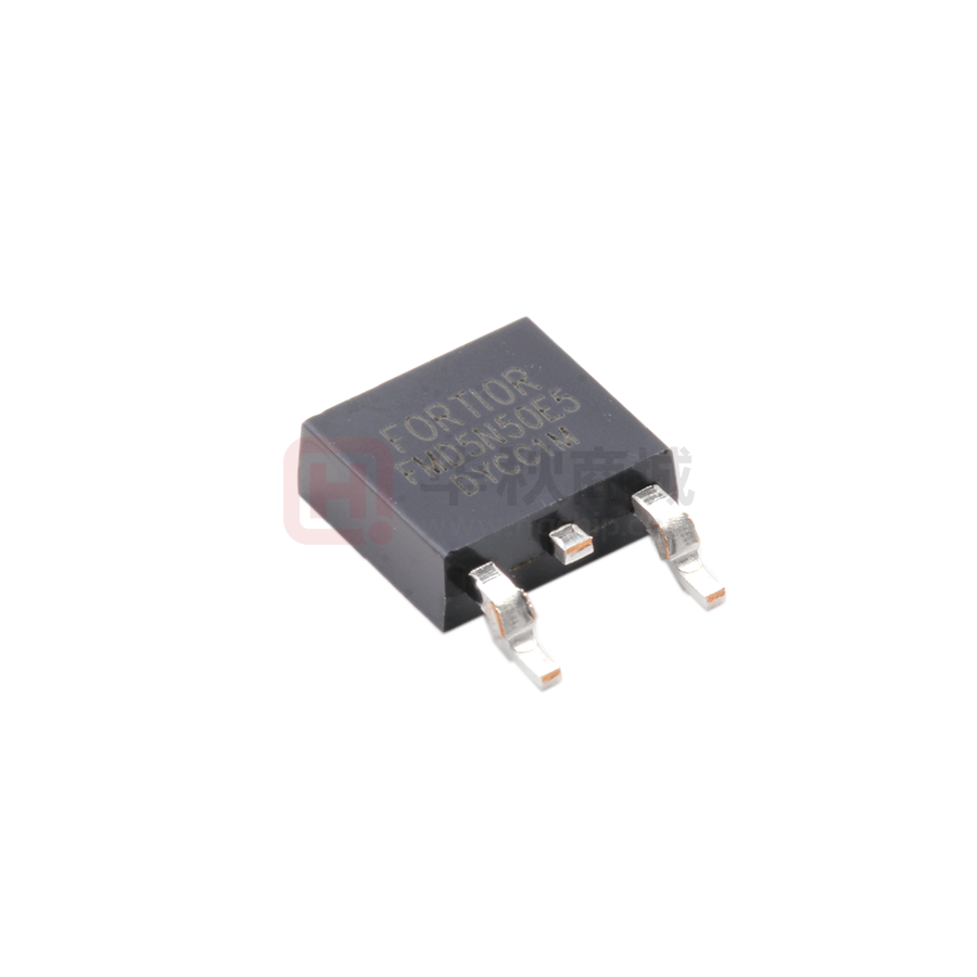
FMD5N50E5
Silicon N-Channel Power MOSFET
General Description:
FMD5N50E5, the silicon N-channel Enhanced VDMOSFETs,
VDSS
500
V
ID
5
A
Trr
85
ns
1.25
Ω
is obtained by the self-aligned planar Technology which reduce
the conduction loss, improve switching performance and
enhance the avalanche energy. The transistor can be used in
RDS(ON)Typ
various power switching circuit for system miniaturization and
higher efficiency. The package form is TO-252, which accords
with the RoHS standard.
Features :
Fast body diode eliminates the need for external
diode in ZVS applications.
Lower Gate charge results in simpler drive
requirements
Higher Gate voltage threshold offers improved noise
immunity
Applications:
Motor Control applications
Uninterruptible Power Supplies
Zero Voltage Switching SMPS
Absolute(Tc=25°C unless otherwise specified)
Symbol
Parameter
VDSS
Drain-to-Source Voltage
a1
V
5
A
2.9
A
Pulsed Drain Current
20
A
Gate-to-Source Voltage
±30
V
a2
Single Pulse Avalanche Energy
350
mJ
a1
Avalanche Energy ,Repetitive
31
mJ
Avalanche Current
2.5
A
Peak Diode Recovery dv/dt
5.0
V/ns
Power Dissipation
75
W
0.60
W/°C
150,–55 to 150
°C
300
°C
VGS
EAS
EAR
a1
dv/dt a3
PD
TJ,T stg
Rev1.0
500
Continuous Drain Current TC = 100 °C
IDM
TL
Units
Continuous Drain Current
ID
IAR
Rating
Derating Factor above 25°C
Operating Junction and Storage Temperature
Range
MaximumTemperature for Soldering
-1-
�FMD5N50E5
Electrical Characteristics(Tc= 25°C unless otherwise specified)
OFF Characteristics
Symbol
VDSS
ΔBVDSS/ΔTJ
I DSS
Parameter
Rating
Test Conditions
Drain to Source Breakdown
Voltage
Bvdss Temperature Coefficient
Typ.
Max.
500
--
--
V
--
0.55
--
V/
°C
VDS =500V, VGS= 0V,
Ta = 25°C
VDS =400V, VGS= 0V,
Ta = 125°C
--
--
1
µA
--
--
10
µA
VGS= 30V
--
--
100
nA
VGS =-30V
--
--
-100
nA
ID=250uA,Reference25°C
IGSS(F)
IGSS(R)
Gate to Source Reverse Leakage
its
Min.
VGS=0V, ID=250µA
Drain to Source Leakage
Current
Gate to Source Forward Leakage
Un
ON Characteristics
Symbol
Parameter
Rating
Test Conditions
RDS(ON)
Drain-to-Source On-Resistance
VGS=10V,ID=2.5A
VGS(TH)
Gate Threshold Voltage
VDS = VGS, ID = 250µA
Min. Typ.
-1.25
-3.0
Units
Max.
1.5
Ω
5.0
V
Pulse width tp≤380µs, δ ≤2%
Dynamic Characteristics
Symbol
Parameter
gfs
Forward Transconductance
Ciss
Input Capacitance
Rating
Test Conditions
VDS=15V, ID =2.5A
VGS =0 V VDS = 25V
f = 1.0MHz
Coss
Output Capacitance
Crss
Reverse Transfer Capacitance
Units
Min.
--
Typ.
5.0
Max.
--
--
775
--
--
79
--
--
9.5
--
S
pF
Resistive Switching Characteristics
Symbol
Parameter
td(ON)
Turn-on Delay Time
tr
Rise Time
td(OFF)
Turn-Off Delay Time
tf
Fall Time
Qg
Total Gate Charge
ID =5A VDD = 250V
RG =25Ω
Qgs
Gate to Source Charge
Qgd
Gate to Drain (“Miller”)Charge
Rev1.0
Rating
Test Conditions
ID = 5A VDD =250V
VGS = 10V
-2-
Units
Min.
--
Typ.
12
Max.
--
--
46
--
--
50
--
--
48
--
--
19
--
4.0
--
8.0
ns
nC
�FMD5N50E5
Source-Drain Diode Characteristics
Symbol
IS
ISM
VSD
trr
Qrr
Parameter
Rating
Test Conditions
Units
Min.
Typ.
Max.
--
--
5
A
--
--
20
A
IS=5.0A,VGS=0V
--
--
1.5
V
Reverse Recovery Time
IS=5.0A,T j = 25°C
--
85
--
ns
Reverse Recovery Charge
dIF/dt=100A/us,
VGS=0V
--
265
--
nC
Continuous Source Current (Body
Diode)
Maximum Pulsed Current (Body
Diode)
Diode Forward Voltage
Pulse width tp ≤380µs, δ ≤2%
Symbol
Parameter
Typ.
Units
RθJC
Junction-to-Case
1.67
℃/W
RθJA
Junction-to-Ambient
62.5
℃/W
a1 Repetitive rating; pulse width limited by maximum junction temperature
a2 L=10mH, ID=8A, Start TJ=25℃
a3 ISD =5A,di/dt ≤100A/us,VDD≤BVDS, Start TJ=25℃
Rev1.0
-3-
�FMD5N50E5
Characteristics Curve
80
PD , Power Dissipation ,Watts
Id , Drain Current , Amps
100
10
1ms
1
10ms
OPERATION IN THIS AREA
MAY BE LIMITED BY RDS(ON)
TJ=MAX RATED
TC=25°C Single Pulse
0 .1
100ms
DC
70
60
50
40
30
20
10
0
0 .0 1
1
10
100
V d s , D ra in -to -S o u rc e V o lta g e , V o lts
1000
0
Figure 1 Maximun Forward Bias Safe Operating Area
125
150
Figure 2 Maximun Power Dissipation vs Case Temperature
6
6
5
Id , Drain Current , Amps
Id , Drain Current , Amps
75
100
50
TC , Case Temperature , °C
25
4
3
2
PULSE DURATION=10µs
DUTY FACTOR=0.5%MAX
Tc =25°C
VGS=15V
4.5
VGS=7V
3
VGS=6V
VGS=6.5V
1.5
VGS=4.5V
VGS=5.5V
1
0
0
0
25
75
1 00
125
50
TC , C a se Te m p e ra tu re , °C
1 50
Figure 3 Maximum Continuous Drain Current vs Case Temperature
0
5
10
15
20
Vds , Drain-to-Source Voltage , Volts
25
Figure 4 Typical Output Characteristics
Thermal Impedance, Normalized
1
50%
20%
0.1 10%
5%
PDM
2%
0.01
Single pulse
0.001
0.00001
1%
NOTES
DUTY FACTOR D=t1/ t2
PEAK Tj=PDM*ZthJC*RthJC+TC
0.0001
0.001
0.01
Rectangular Pulse Duration,Seconds
Figure 5 Maximum Effective Thermal Impendance , Junction to Case
Rev1.0
t1
t2
-4-
0.1
1
�FD5N50E5
100
FOR TEMPERATURES
ABOVE 25°C DERATE
PEAK CURRENT AS
FOLLOWS:
Idm , Peak Current , Amps
TRANSCONDUCTANCE MAY LIMIT
CURRENT IN THIS REGION
150 TC
I I 25
125
10
1
1.00E-05
1.00E-04
1.00E-03
Rds(on), Drain to Source ON
Resistance , Ohms
PULSE DURATION = 10µs
DUTY CYCLE = 0.5%MAX
VDS=30V
7.5
6
4.5
3
-55°C
+25°C
1.5
+150°C
0
3
4
5
Vgs , Gate to Source Voltage , Volts
1.00E+01
PULSE DURATION = 10µs
DUTY FACTOR = 0.5%MAX
Tc =25°C
5
4
ID= 5A
ID= 2.5A
3
ID= 1.25A
2
1
6
Rds(on), Drain to Source ON Resistance,
Nomalized
3
PULSE DURATION = 10µs
DUTY CYCLE= 0.5%MAX
Tc =25°C
2.5
VGS=20V
2
4
6
8
10
12
Vgs , Gate to Source Voltage,Volts
14
Figure 8 Typical Drain to Source ON Resistance vs Gate Voltage
and Drain Current
Figure 7 Typical Transfer Characteristics
Rds(on), Drain to Source ON
Resistance, Ohms
1.00E+00
0
2
1.5
2.5
2.25
2
PULSE DURATION = 10µs
DUTY CYCLE= 0.5%MAX
VGS=10V ID=2.5A
1.75
1.5
1.25
1
0.75
0.5
1
0
1
2
3
Id , Drain Current , Amps
4
-50
0
50
100
Tj, Junction temperature , C
Figure 10 Typical Drian to Source on Resistance
vs Junction Temperature
Figure 9 Typical Drain to Source ON Resistance
vs Drain Current
Rev1.0
1.00E-01
Figure 6 Maximun Peak Current Capability
6
9
Id , Drain Current , Amps
1.00E-02
t ,Pulse Width , Seconds
-5-
150
�FMD5N50E5
1.1
1.1
Bvdss,Drain to Source
Breakdown Voltage, Normalized
Vgs(th),Threshold Voltage, Nomalized
1.15
1.05
1
0.95
0.9
0.85
0.8
0.75
VGS=0V
ID=250µA
0.7
0.65
-75
1.05
1
0.95
0.9
-50
-25
0
25 50 75 100 125 150 175
Tj, Junction temperature , °C
-55
10000
-5
20
45
70
95 120
Tj, Junction temperature , °C
145
170
Vgs , Gate to Source Voltage ,Volts
12
1000
Ciss
Coss
100
Crss
10
VGS=0V , f=1MHz
Ciss=Cgs+Cgd
Coss=Cds+Cgd
Crss=Cgd
1
VDS=150V
VDS=250V
VDS=400V
10
8
6
4
2
ID=5.0A
0
0.1
1
10
Vds , Drain - Source Voltage , Volts
100
0
Figure 13 Typical Capacitance vs Drain to Source Voltage
2
4
6
8
10 12 14
Qg , Total Gate Charge , nC
16
18
20
Figure 14 Typical Gate Charge vs Gate to Source Voltage
8
100
7
Id , Drain Current , Amps
Isd, Reverse Drain Current , Amps
-30
Figure 12 Typical Breakdown Voltage vs Junction Temperature
Figure 11 Typical Theshold Voltage vs Junction Temperature
Capacitance , pF
VGS=0V
ID=250µA
6
5
4
3
+150°C
2
+25°C
0.2
0.4
0.6
0.8
1
Vsd , Source - Drain Voltage , Volts
1.2
1
Figure 16 Unclamped Inductive Switching Capability
Figure 15 Typical Body Diode Transfer Characteristics
Rev1.0
STARTING Tj = 150°C
0.1
1.00E-06 1.00E-05 1.00E-04 1.00E-03 1.00E-02 1.00E-01 1.00E+00
tav,Time in Avalanche,Seconds
0
0
10
If R=0: tAV=(L* IAS) / (1.38VDSS-VDD)
If R≠0: tAV=(L/R) In[IAS*R/ (1.38VDSS-VDD)+1]
R equals total Series resistance of Drain circuit
-55°C
1
STARTING Tj = 25°C
-6-
�FMD5N50E5
TestCircuitandWaveform
Rev1.0
-7-
�FD5N50E5
Rev1.0
-8-
�FD5N50E5
Package Information
Values(mm)
Items
MIN
MAX
A
6.30
6.80
B
5.20
6.20
C
2.10
2.50
D
0.40
0.60
E1
0.60
0.80
E2
0.70
0.90
F
0.40
0.60
G
0.80
1.00
L1
9.70
10.20
L2
2.70
3.10
H
0.60
0.90
M
5.10
5.50
N
2.09
2.49
R
0.3
T
1.40
1.60
Y
5.10
6.30
TO-252 Package
Rev1.0
-9-
�FMD5N50E5
The name and content of poisonous and harmful material in products
Part’s Name
Limit
Hazardous
Pb
≤0.1%
Substance
Hg
Cd
Cr(VI)
PBB
PBDE
≤0.1%
≤0.01%
≤0.1%
≤0.1%
≤0.1%
Lead Frame
O
O
O
O
O
O
Molding Compound
O
O
O
O
O
O
Chip
O
O
O
O
O
O
Wire Bonding
O
O
O
O
O
O
Solder
X
O
O
O
O
O
O means the hazardous material is under the criterion of SJ/T11363-2006.
X means the hazardous material exceeds the criterion of SJ/T11363-2006.
Note
The plumbum element of solder exist in products presently, but within the allowed
range of Eurogroup’s RoHS.
Warnings
1. Exceeding the maximun ratings of the device in performance may cause damage to the device, even the
permanent failure, which may affect the dependability of the machine. It is suggested to be used under 80
percent of the maximun ratings of the device.
2. When installing the heatsink, please pay attention to the torsional moment and the smoothness of the heatsink.
3.
VDMOSFETs is the device which is sensitive to the static electricity, it is necessory to protect the device
from being damaged by the static electricity when using it.
4.
Rev1.0
This publication is made by Fortior technology and subject to regular change without notice.
- 10 -
�