MT613X
Omni-polar, Low Power, 360 Degree Switch IC
1 Product Description
The MT613X family is produced with monolithic
technology,which builds AMR sensor & ASIC on one
chip. The IC internally includes a Wheatstone bridge
with magnetic film, a current regulator for operating
with supply voltage from 1.65V to 5.0V, a sleep/awake
logic for low power consumption requirement, small
signal amplifier and Schmitt trigger comparator with
dynamic offset cancellation, and an output driver with
push pull output.
When combined with a magnet, it becomes a noncontact switch with low power consumption, high
sensitivity and high reliability. All directions of
horizontal magnetic field parallel to the electrode of
the package can be detected by an arbitrary polarity.
4 Application
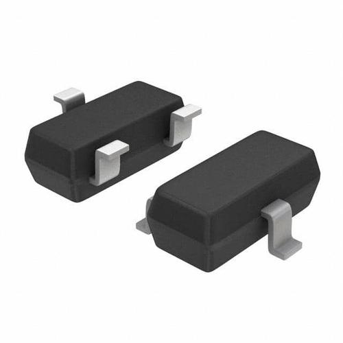
The MT613X family provide SOT-23 for surface mount,
RoHS compliant.
2 Features
■
■
■
■
■
■
■
■
■
Home appliances, Industrial
Position Detection
Proximity Switch
Smart Meter
Speed Detection
Handheld Device
Consumer Device
5. Pin Configuration and Functions
VCC
Out
GND
SOT-23
1
2
3
Description
Power
Output
Push Pull or
Open Drain
SOT-23
Top-View
GND
3
■
■
Monolithic Technology
360 Degree AMR (Anisotropic Magneto Resistance)
Omni-polar Switch
1.65~5.0V Operating Vcc Range
-40℃~125℃ Operating Temperature
Package Option:
SOT-23
Magnetic Sensitivity Option:
BOP=±18Gs, BRP=±13Gs
Push Pull & Open Drain Output Option:
MT6131 & MT6132: Push Pull
MT6133 & MT6135: Open Drain
Operation Frequency Option:
MT6131 & MT6133: 20Hz
MT6132 & MT6135: 1KHz
Low Power Consumption
RoHS Compliant: (EU)2015/863
■
■
■
■
■
■
■
按钮
SOT-23, tape & reel
(3000pcs/bag)
OUT
MT613XAT
2
Description
Vcc
Part No.
1
3 Product Overview of MT613X
Figure.1
Pin Configuration
TO-92& Functions
Top-View
magntek.com.cn | Magnetic Tech Makes Magic Change
1
Rev
1.1
Ground
�MT613X
Omni-polar, Low Power, 360 Degree Switch IC
Table of Contents
1
Product Description………….……………...…….……...…………………………………….…….………1
2
Features……………………………….……..……………………………………………………………….…….1
3
Product Overview of MT613X ..……………….…………………………………………………………1
4
Applications……………………………………………………………………………………………………….1
5
Pin Configuration and Functions…………………………………………………….………………….1
6
Definition of Switching Function……………………………………………………………………….3
7
Function Description…......…………………………………………………………………………………..3
8
Feature Description……………………………………………………………………………………………3
9
Functional Block Diagram…………………………………………………………………………………..4
10
Electrical and Magnetic Characteristics………………………………………………………………5
10.1 Absolute Maximum Ratings……………………………………………………………………………….5
10.2 Electrical Specifications………………………………….………………………………………………..5
10.3 Magnetic Characteristics……………………………………………………………………………………6
10.4 ESD Ratings………………………………………………………………………………………………………..6
10.5 Characteristic Performance………………………………………………………………….…………….6
10.6 Typical Output Waveform…………………………………………………………………………………..7
11
Typical Application Circuit………………………………………………………………………………….7
12
Power on Output Waveform………………………………………………………………………………8
13
Package Material Information……………………………………………………………………………9
13.1 SOT-23 Package Information……………………………...………………………………………………9
14
1
2
Copy Rights and Disclaimer……………………………………………………………………………..10
Originally Version
1.1 Version
Reversion History
magntek.com.cn | Magnetic Tech Makes Magic Change
Update supply current
Update the marking spec of SOT-23
2
Rev
1.1
�MT613X
Omni-polar, Low Power, 360 Degree Switch IC
6 Definition of Switching Function
Figure.2 shows the device functionality and hysteresis
Vcc
North
Figure.2
BOP N BRP N
BRP S
BOP S
South
Omni-polar Switching Function
7 Function Description
BOP: Operating Point, Magnetic flux density applied on the branded side of the package which turns the
output driver ON (VOUT=Low)
BRP: Releasing Point, Magnetic flux density applied on the branded side of the package which turns the
output driver OFF (VOUT=High)
BHYST: Hysteresis Window, |BOP - BRP|
8 Feature Description
The MT613X series is sensitive to the magnetic field that is parallel to the package (X & Y axis). To operate
the MR switch, the magnetic field should be applied to the sensor parallel to the package. MT613X series
detect the magnetic field in any parallel direction, but it does not respond to magnetic field in the vertical
direction.
GND
3
按钮
1
2
Vcc
OUT
Figure.3
Direction of magnetic field
(N or S)
Detection of magnetic field
magntek.com.cn | Magnetic Tech Makes Magic Change
3
Rev
1.1
�MT613X
Omni-polar, Low Power, 360 Degree Switch IC
9 Functional Block Diagram
Vcc
Sleep/Awake
Logic
Regulator
ESD
Dynamic
Offset
Cancellation
Out
AMR
AMP
COMP
Output Driver
AMR
GND
Figure.4
Functional Block Diagram (MT6131 & MT6132)
Vcc
Sleep/Awake
Logic
Regulator
ESD
Dynamic
Offset
Cancellation
Out
AMR
AMP
COMP
Output Driver
AMR
GND
Figure.5
Functional Block Diagram (MT6133 & MT6135)
magntek.com.cn | Magnetic Tech Makes Magic Change
4
Rev
1.1
�MT613X
Omni-polar, Low Power, 360 Degree Switch IC
10 Electrical and Magnetic Characteristics
10.1 Absolute Maximum Ratings
Absolute maximum ratings are limited values to be applied individually, and beyond which the
serviceability of the circuit may be impaired. Functional operability is not necessarily implied. Exposure to
absolute maximum rating conditions for an extended period of time may affect device reliability.
Symbol
Parameters
Min
Max
Units
VCC
Supply Voltage
-
7
V
VRCC
Reverse Battery Voltage
-0.4
-
V
VOUT
Output Voltage
-
7
V
IOUT
Continuous Output Current
-
20
mA
TA
Operating Ambient Temperature
-40
125
℃
TS
Storage Temperature
-50
150
℃
TJ
Junction Temperature
-
165
℃
B
Magnetic Flux Density
1200
Gs
10.2 Electrical Specifications
At TA=-40~125℃, VCC=1.65V~5.0V (unless otherwise specified)
Symbol
Parameters
Test Condition
Min
Typ
Max
Unit
VCC
Supply Voltage
Operating
1.65
3.60
5.00
V
MT6131 & MT6133, VCC=3.6V,
∣B∣∣BOP∣
-
-
0.4
V
IOFF
Output Leakage
Current
VOUT=5V, ∣B∣3.6V/us, B>BOP(MAX)
-
80
120
us
MT6131 & MT6133, VCC=3.6V
10
20
-
Hz
MT6132 & MT6135, VCC=3.6V
0.5K
1K
-
Hz
VCC=3.6V
-
16
-
us
MT6131 & MT6133, VCC=3.6V
-
50
-
ms
MT6132 & MT6135, VCC=3.6V
-
1
-
ms
MT6131 & MT6133, VCC=3.6V
-
0.03
-
%
MT6132 & MT6135, VCC=3.6V
-
1.50
-
%
-
301
-
℃/W
FOP
Operation Frequency
TAW
Awake Time
TSL
Sleep Time
D.C.
Duty Cycle
RTH
Thermal Resistance of SOT-23
magntek.com.cn | Magnetic Tech Makes Magic Change
5
Rev
1.1
�MT613X
Omni-polar, Low Power, 360 Degree Switch IC
10.3 Magnetic Characteristics
At TA =25℃, VCC=1.65V~5.0V (unless otherwise specified)
Part No.
Symbol
MT613X Series
Min
Typ
Max
Unit
BOP
-
±18
±28
Gs
BRP
±3
±13
-
Gs
-
5
-
Gs
BHYST
10.4 ESD Ratings
Symbol
VESD
Reference
Values
Unit
Human-body model (HBM)
AEC-Q100-002
4000
V
Charged-device model (CDM)
AEC-Q100-011
1000
V
10.5 Characteristic Performance
5
Supply Current (uA)
4.5
4
3.5
3
Vcc=1.65V
2.5
2
Vcc=3.6V
1.5
Vcc=5.0V
1
0.5
0
-40
125
30
Bop (90 Degree)
Brp (90 Degree)
Bop (180 Degree)
Brp (180 Degree)
15
25
20
15
10
5
0
Bhyst (90 Degree)
Bhyst (180 Degree)
12
9
6
3
0
-40
Figure.7
150
Supply Current vs. Temperature
35
Magnetic Field Intensity (Gs)
85
Magnetic Field Intensity (Gs)
Figure.6
25
25
85
125
150
Magnetic Characteristics vs. Temperature
-40
℃
Figure.8
25
85
125
150
Magnetic Characteristics vs. Temperature
(BOP & BRP) (At VCC=3.6V)
(BHYST) (At VCC=3.6V)
Magnetic Field @ 90 Degree & 180 Degree
Magnetic Field @ 90 Degree & 180 Degree
magntek.com.cn | Magnetic Tech Makes Magic Change
6
Rev
1.1
℃
�MT613X
Omni-polar, Low Power, 360 Degree Switch IC
10.5 Characteristic Performance (continued)
330
315
300
285
34525
0
15
20
30
45
15
60
10
75
5
270
90
0
255
105
240
225
210
Figure.9
Bop
Brp
120
195
180
165
135
150
360 Degree Magnetic Characteristics (At VCC=3.6V, TA=25 ℃)
10.6 Typical Output Waveform
MT6131AT as example
B
Sampling Pulse
Magnetic Flux
BOP S
BRP S
T
BRP N
BOP N
On
Off
Output
V
High
Low
T
Note: Output is not immediately updated until the chip wakes up from sleep mode and samples the input
Figure.10
Digital Output vs. Magnetic Flux Density & Sampling Pulse
magntek.com.cn | Magnetic Tech Makes Magic Change
7
Rev
1.1
�MT613X
Omni-polar, Low Power, 360 Degree Switch IC
11 Typical Application Circuit
C1=100nF
C1=100nF
Vcc
OUT
3
GND
RL = 100kΩ
1
按钮
Vcc
GND
2
Out
Vcc
1
按钮
Vcc
OUT
GND
GND
2
Out
C2=1nF
Figure.11
3
C2=1nF
Typical Application Circuit
Figure.12
Typical Application Circuit
Push Pull Output
Open Drain Output
MT6131 & MT 6132
MT6133 & MT 6135
12 Power on Output Waveform
Output
Magnetic Flux
VCC
VCC rise time < 1us, TPO is the time from the stable point of VCC to the valid point of output
Figure.13
∣B∣>∣BOP∣
∣B∣
很抱歉,暂时无法提供与“MT6131AT”相匹配的价格&库存,您可以联系我们找货
免费人工找货- 国内价格
- 5+2.27880
- 50+1.73880
- 150+1.50120
- 500+1.36080
- 3000+1.23120
- 6000+1.15560
- 国内价格
- 50+1.42062
- 500+1.36133