Integrated in
OVP&OCP products
provider
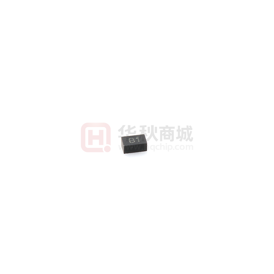
WPE0501P1
1-Line Bi-directional Low Capacitance TVS Diode
Description
Mechanical Characteristics
The WPE0501P1 is a bi-directional TVS diode, utilizing
Package: DFN1006-2 (1.0×0.6×0.5mm)
leading monolithic silicon technology to provide fast re-
Lead Finish: NiPdAu
sponse time, very low capacitance and low ESD
Case Material: “Green” Molding Compound.
clamping voltage, making this device an ideal solution
UL Flammability Classification Rating 94V-0
for protect- ing voltage sensitive data and power line.
Moisture Sensitivity: Level 3 per J-STD-020
Terminal Connections: See Diagram Below
The WP E 0 50 1 P 1 complies with the IEC 61000-4-2
(ESD)
standard with ±25kV air and ±22kV contact
Marking Information: See Below
discharge. It is assembled into an ultra-small
1.0x0.6x0.5mm lead-free DFN pack- age. The small size
Applications
and very low capacitance make WPE0501P1 an ideal
choice to protect cell phone, digital cameras, audio
Cellular Handsets and Accessories
players, data interface and many other portable
Personal Digital Assistants
Notebooks and Handhelds
Portable Instrumentation
Digital Cameras
Peripherals
Audio Players
Keypads, Side Keys, USB 2.0, LCD Displays
applications.
Features
Ultra small package: 1.0x0.6x0.5mm
Protects one data or power line
Ultra low leakage: nA level
Working voltage: 5V
Low clamping voltage
2-pin leadless package
Complies with following standards:
– IEC 61000-4-2 (ESD) immunity test
Marking information
Air discharge: ±25kV
Details marking code reference customer approval list
Contact discharge: ±22kV
– IEC61000-4-4 (EFT) 40A (5/50ns)
Ordering Information
RoHS Compliant
Dimensions & Symbol(Unit: mm Max)
Rev.A_Aug,2016
Part Number
WPE0501P1
-1-
Packaging
10000/Tape & Reel
Reel Size
7 inch
www.wpmtek.com
�WPE0501P1
Integrated in
OVP&OCP products
provider
1-Line Bi-directional Low Capacitance TVS Diode
Absolute maximum ratings (TA=25ºC, RH=45%-75%, unless otherwise noted)
Parameter
Symbol
ESD per IEC 61000−4−2 (Air)
Value
±25
VESD
ESD per IEC 61000−4−2 (Contact)
Operating Temperature Range
Storage Temperature Range
Unit
kV
±22
TJ
−55 to +125
°C
Tstg
−55 to +150
°C
Electrical characteristics (TA=25℃)
Parameter
Reverse Working Voltage
Breakdown Voltage
Symbol
Min
Typ
VRWM
VBR
6.0
Max
Unit
Test Condition
5.0
V
8.0
V
IT = 1mA
Reverse Leakage Current
IR
0.2
µA
VRWM = 5.0V
Clamping Voltage
VC
8
V
IPP = 1A (8 x 20µs pulse)
Clamping Voltage
VC
10
V
IPP = 3A (8 x 20µs pulse)
Junction Capacitance
CJ
pF
VR = 0V, f = 1MHz
Rev.A_Aug,2016
5.5
-2-
www.wpmtek.com
�Integrated in
OVP&OCP products
provider
WPE0501P1
1-Line Bi-directional Low Capacitance TVS Diode
Typical Performance Characteristics (TA=25°C unless otherwise Specified)
Junction Capacitance vs. Reverse Voltage
Peak Pulse Power vs. Pulse Time
Clamping Voltage vs. Peak Pulse Current
Power Derating Curve
200
Voltage (V)
150
TA = 25OC
Corre
rrected for 20dB
attenuator 1M Ohm
100
50
0
-50
-20
0
20 Time (ns) 40
60
80
ESD Clamping Voltage
8 X 20μs Pulse Waveform
Rev.A_Aug,2016
-3-
8 kV Contact per IEC61000−4−2
www.wpmtek.com
�Integrated in
OVP&OCP products
provider
WPE0501P1
1-Line Bi-directional Low Capacitance TVS Diode
Soldering parameters
Pb-Free assembly
(see FIG.2)
Reflow Condition
Pre Heat
-Temperature Min (Ts(min))
+150℃
-Temperature Max(Ts(max))
+200℃
-Time (Min to Max) (ts)
60-180 secs.
Average ramp up rate (Liquid us Temp (TL) to peak)
3℃/sec. Max
Ts(max) to TL - Ramp-up Rate
3℃/sec. Max
Reflow
-Temperature(TL) (Liquid us)
+217℃
-Temperature(tL)
60-150 secs.
Peak Temp (Tp)
+260(+0/-5)℃
Time within 5℃ of actual Peak Temp (tp)
30 secs. Max
Ramp-down Rate
6℃/sec. Max
Time 25℃ to Peak Temp (TP)
8 min. Max
Do not exceed
+260℃
Rev.A_Aug,2016
-4-
www.wpmtek.com
�WPE0501P1
Integrated in
OVP&OCP products
provider
1-Line Bi-directional Low Capacitance TVS Diode
Package mechanical data
DIMENSIONS
SYM
MILLIMETERS
NOM
MAX
0.50
0.55
A
A1
0.00
0.02
0.05
0.000
0.001
0.002
b
0.45
0.50
0.55
0.018
0.020
0.022
c
0.12
0.15
0.18
0.005
0.006
0.007
D
0.95
1.00
1.05
0.037
0.039
0.041
e
MIN
0.018
INCHES
NOM
0.020
MIN
0.45
0.65 BSC
MAX
0.022
0.026 BSC
E
0.55
0.60
0.65
0.022
0.024
0.026
L
0.20
0.25
0.30
0.008
0.010
0.012
h
0.07
0.12
0.17
0.003
0.005
0.007
Suggested Land Pattern
DIMENSIONS
SYM
MILLIMETERS
INCHES
X
0.60
0.024
Y1
0.50
0.020
Y2
0.30
0.012
Y3
0.80
0.032
Z
1.30
0.052
Contact information
WPMTEK Incorporated Limited
Floor 1 Building 4#, Binxianghua Industry Park, No.7,
Huada Road, Hualian Community, Longhua New District, Shenzhen
TEL:86755-29308003
FAX:86755-23739900
wpmtek Incorporated Limited (WPM) reserves the right to make changes to the product specification and data in this document without notice. WPM
makes no warranty, representation or guarantee regarding the suitability of its products for any particular purpose, nor does WPM assume any liability
arising from the application or use of any products or circuits, and specifically dis- claims any and all liability, including without limitation special,
consequential or incidental damages.
Rev.A_Aug,2016
-5-
www.wpmtek.com
�
很抱歉,暂时无法提供与“WPE0501P1”相匹配的价格&库存,您可以联系我们找货
免费人工找货- 国内价格
- 1+0.06000
- 100+0.05600
- 300+0.05200
- 500+0.04800
- 2000+0.04600
- 5000+0.04480
- 国内价格
- 50+0.11790
- 500+0.09184
- 1500+0.07736
- 10000+0.06865
- 20000+0.06115
- 50000+0.05715
- 国内价格
- 1+0.30250
- 500+0.10065
- 5000+0.06710
- 10000+0.05489
