Level: Public Information
HY-40R201
1 Bluetooth BLE 5.0 Module Specifications
(40 pin)
11 Nov. 2017
Version:V2.2
Copyright © 2010-2017
7 SHENGRUN Technology Co., Ltd.
All rights reserved.
SHENGRUN Technologies assumes no responsibility for any errors which may appear in
this manual, Furthermore, SHENGRUN Technologies reserves the right to alter the
hardware, software, and/or specifications detailed here at any time wit
without
hout notice and does
not make any commitment to update the information contained here. SHENGRUN’s
SHENGRUN
products are not authorized for use as critical components in life support devices or systems.
SHENGRUN Technologies assumes no responsibility for any patents
s or authorized the use
of intellectual property rights.
The Bluetooth trademark is owned by the Bluetooth SIG Inc., USA
�HY-40R201
40 pin module
Version History
Version
V1.0
Revision
Date
09/08/2017
Reviser
Reviewer
GKL
LYC
Revised Contents
1st issue
1. Added English address map.
2. Added ceramic antenna model and
V2.0
17/10/2017
WF/ZLL
LYC
changed Model No.
3. Added application note
4. Added FCC ID No.
5. Changed document format.
V2.1
25/10/2017
WF
LYC
V2.2
11/11/2017
WF
LYC
1.Added RF Regurations pre-certified
description; And Canada IC No.
1.Correct: 5. Pinout and GPIO function
Description UART RX/TX GIO Port pin.
�HY-40R201
40 pin module
CONTENTS
1. DESCRIPTION ........................................................................................................................................................1
1-1.APPLICATIONS: ........................................................................................................................................................... 1
1-2.KEY FEATURES: ........................................................................................................................................................... 1
2. PRODUCT MODEL NUMBER:
HARDWARE MODEL DESCRIPTION ...........................................................2
2-1. (4 KINDS ANTENNA TYPE FOR CHOICE) ,(OPTION: WITH SHIELD CASE OR NO SHIELD CASE) ............................................................ 2
2-2: FCC ID &( IC ID/ WAIT DEFIND) PRINT FORMAT ON THE SHIELD CASE :( HY-40R201PC MODEL ONLY) ........................................ 2
3. PCBA DIMENSION SIZE AND PICTURE .............................................................................................................2
3-1: HY-40R201P / WMD40R201SR6P0( PCB IFAANTENNA) ............................................................................................... 2
&HY-40R201PC / WMD40R201SR6PC (PCB IFAANTENNA, WITH SHIELD CASE);....................................................................... 2
3-2:HY-40R201I / WMD40R201SR6I0(IPEX RF CONNECTOR TERMINAL) ................................................................................. 3
&HY-40R201IC / WMD40R201SR6IC (IPEX RF CONNECTOR WITH SHIELD CASE )....................................................................... 3
3-3: HY-40R201W / WMD40R201SR6W0( METAL WIREANTENNA)(1/4Λ HALF WAVE DIPOLE)_ ................................................. 3
&HY-40R201WC / WMD40R201SR6WC ( METAL WIRE ANTENNA, WITH SHIELD CASE) ; ......................................................... 3
3-4: HY-40R201C / WMD40R201SR6C0( CERAMICANTENNA) ............................................................................................... 3
&HY-40R201CC / WMD40R201SR6CC (CERAMIC ANTENNA, WITH SHIELD CASE) ; .................................................................. 3
4.APPLICATION NOTE: .............................................................................................................................................4
5. PINOUT AND GPIOFUNCTION DESCRIPTION .................................................................................................5
6. ELECTRICAL CHARACTERISTICS ......................................................................................................................6
6-1.RADIO PERFORMANCE & CURRENT CONSUMPTION ................................................................................................................ 7
6-2. ABSOLUTE MAXIMUM RATINGS ........................................................................................................................................ 7
6-3. ESD RATINGS ................................................................................................................................................................ 7
6-4. RECOMMENDED OPERATING CONDITIONS........................................................................................................................... 8
6-5.GPIODC CHARACTERISTICS .............................................................................................................................................. 8
6-6. TIMING REQUIREMENTS .................................................................................................................................................. 8
6-7. SWITCHING CHARACTERISTICS........................................................................................................................................... 9
7. BLOCK DIAGRAM ..................................................................................................................................................9
8. FUNCTIONAL BLOCK DIAGRAM .........................................................................................................................9
9. WORKING
MODE SCHEMATIC .......................................................................................................................10
10. RECOMMEND REFLOW PROFILE( LEADLESS SOLDER CREAM: SN 96.5%, AG 3%, CU 0.5%) .........10
11.HY-40R201PC/WMD40R201SR6PC MODULE
FCC/INDUSTRY CANADA STATEMENT ....................... 11
12.CONTACT US ......................................................................................................................................................13
�HY-40R201
40 pin module
1. Description
HY-40R201 Bluetooth low energy single mode module is a single mode device targeted for low
power sensors and accessories.
HY-40R201 offers all Bluetooth low energy features: radio, stack, profiles and application space for
customer applications. The module also provides flexible hardware interfaces to connect sensors.
HY-40R201 can be powered directly with a standard 3V coin cell batteries or pair of AAA batteries.
in lowest power shutdown mode it consumes only 0.15uA and will wake up in few microseconds.
HY-40R201 transmission distance of 100 meter or more. (At face to face, free space, 1.2 Meter high
from Ground for testing).
Bluetooth IC:TTC2640R2 6*6*0.9mm 48pin IC,Used TI CC2640R2 die chip
1-1.APPLICATIONS:
Heart rate sensors
Pedometers
Watches
Blood pressure and glucose meters
Weight scales
Key fobs
Households sensors and collector devices
Security tags
Wireless keys (keyless go)
Proximity sensors
HID keyboards and mice
Indoor GPS broadcasting devices
1-2.KEY FEATURES:
Bluetooth v.5.0 single mode compliant
Supports master,slaveand master/slave modes
Integrated Bluetooth low energy stack
GAP, GATT, L2CAP, SMP Bluetooth low energy profiles
Pre-certified RF regurations for BQB BLE 5.0, CE ETSI RED, FCC, IC(Canada), (FCC and
IC certified only for HY-40R201PC PCB antenna with shield case model);
Another can Compliance for worldwide RF Regulations.
Transmit power :+5 dBm typical
Receiver sensitivity: -97dBm typical
Ultra low current consumption :Shutdown. No clocks running, no retention: 150 nA(Typical)
Programmable ARM Cortex-M3 processor for embedding full applications
1 /16
V1.0www.tuner168.com
�HY-40R201
40 pin module
2. Product model Number:
Hardware Model Description
2-1. (4 kinds Antenna type for choice) ,(Option: with shield case or no shield case)
Product Mode Item
PCB NO.
Description
1 WMD40R201SR6P0
HY-40R201P
PCB Helix Antenna
2 WMD40R201SR6I0
HY-40R201I
IPEX Connector for External Antenna
3 WMD40R201SR6W0
HY-40R201W
Metal Wire Antenna(λ/4 Half wave dipole)
4 WMD40R201SR6C0
HY-40R201C
Ceramic Antenna
6 WMD40R201SR6PC
HY-40R201PC
PCB Helix Antenna with shield case
5 WMD40R201SR6IC
HY-40R201IC
IPEX Connector for External Antenna with
shield case
7 WMD40R201SR6WC
HY-40R201WC
Metal Wire Antenna with shield case
8 WMD40R201SR6CC
HY-40R201CC
CeramicAntenna with shield case
2-2: FCC ID &( IC ID/ wait defind) Print Format on the Shield Case :( HY-40R201PC model only)
Model:HY-40R201PC
FCC ID:2ADXE-HY-40R201PC
IC :
23267-HY40R201PC
Shield Case Size:
13.0*18.4*1.5mm
Word Type: Calibri
Direction: Horizon
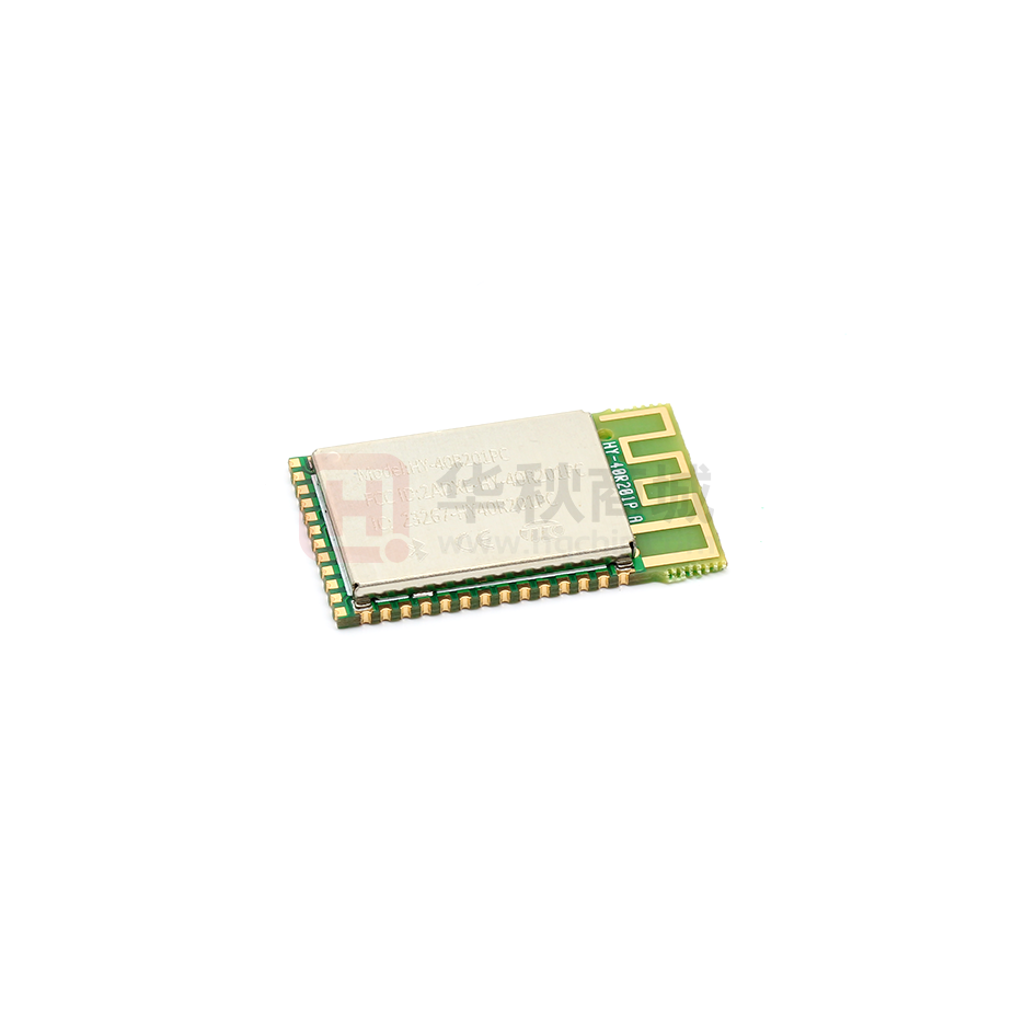
3. PCBA dimension size and picture
3-1: HY-40R201P / WMD40R201SR6P0( PCB IFAAntenna)
&HY-40R201PC / WMD40R201SR6PC (PCB IFAAntenna, with shield case);
(PCBA dimension size : ( 25.16*15.22*2.0/2.6 mm ).
2 /16
V1.0www.tuner168.com
�HY-40R201
40 pin module
3-2:HY-40R201I / WMD40R201SR6I0(IPEX RF connector terminal)
&HY-40R201IC / WMD40R201SR6IC (IPEX RF connector with shield case )
(PCBA dimension size : 25.16*15.22*2.6 mm).
3-3: HY-40R201W / WMD40R201SR6W0( Metal WireAntenna)(1/4λ half wave dipole)_
&HY-40R201WC / WMD40R201SR6WC ( Metal Wire Antenna, with shield case) ;
(PCBA dimension size : 23.2*15.22*2.0/2.6 mm).
3-4: HY-40R201C / WMD40R201SR6C0( CeramicAntenna)
&HY-40R201CC / WMD40R201SR6CC (Ceramic Antenna, with shield case) ;
(PCBA dimension size : 25.16 * 15.22 * 2.0/2.6 mm ).
3 /16
V1.0www.tuner168.com
�HY-40R201
40 pin module
4.Application Note:
4-1.Attention to the electrostatic protection, prevent the soldering iron
and the equipment grounding bad; And the workbench, working environment,
packaging materials and from the human bodyTouch with static electricity,
etc., destroy IC and software be fly; Manual welding module solder iron
temperature, should pay attention to avoid the PCB copper stripping
off;Soldering iron strictlyGrounding requirements, eliminating iron
power failure module;
4-2.Attention to avoid the overall motherboard power supply circuit of bad
welding connected to short circuit or open circuit, causing the bluetooth
chip, abnormal voltage,Thesoftwarewill fly and problems of IC was damaged.
4-3.When programming firm ware , the VDDS supply voltage must in DC 2.4~3.3V,
To avoid programming has not completely, and abnormal status occur..
4-4. Use the module in the production and the transport process, please
insure module’scomponent protection, prevent the precision parts on the
moduleDamaged (welding furnace exit and assembly, testing, delivery process,
suggest using collision buffer material, not collide with each other)
4-5. The module for the humidity sensitive components, if used in SMT reflow
soldering operations, please strictly follow the IPC/JEDECJ - STD - 020
regulation, completes the drying dehumidifying , and for this module has
second processing work after placed in the functional test environment,
the humidity of the chip is no guarantee that in a certain ratio, the honored
guest please understand;(The attention note show in below Fig.)
4-6. The diagram (show in below Fig.) of the module application on external filter parts, whenneed,
please design in the mainboard, the parts parameter can depend on the actual need to changes.
4 /16
V1.0www.tuner168.com
�HY-40R201
40 pin module
4-7.Assembly recommendation 1: Underneath the module antenna and RF circuit on themain
boardPCB copper need to clearance, and place close to the main board edge, as show in below Fig.
The antenna can't be near aroundmetal parts and prevent material existence of electromagnetic
radiation , Can affect the manipulation of the distance.
4-8. Assembly recommendation 2: Signal trace and power supply trace, don't cross layout, as show
in below Fig.To avoid crosstalk, affect the receiving sensitivity.
The module assemble in the motherboard,
must pay attention to:
Around the antenna and all layer’s copper
must be clear, Module antenna should be on
the edge, And there are no metal or obstruct
electromagnetic radiation material to
surround antenna area.
5. Pinout and GPIOfunction Description
Pin
Name
Type
Function Description
1
GND
Power GND
Ground
2
DIO_0
Digital I/O
GPIO, Sensor Controller (I:4mA max)
3
DIO_1
Digital I/O
GPIO, Sensor Controller (I:4mA max)
4
DIO_2
Digital I/O
UART RX;
GPIO, Sensor Controller (I:4mA max)
5
DIO_3
Digital I/O
6
DIO_4
Digital I/O
7
DIO_5
Digital I/O
8
DIO_6
Digital I/O
9
DIO_7
Digital I/O
10
DIO_8
Digital I/O
UART TX;
GPIO, Sensor Controller (I:4mA max)
WAKE UP; Don't floating
GPIO, Sensor Controller (I:4mA max)
GPIO, Sensor Controller, high-drive capability (8mA
max).
GPIO, Sensor Controller, high-drive capability (8mA
max).
GPIO, Sensor Controller, high-drive capability (8mA
max).
GPIO (I: 4mA max)
11
DIO_9
Digital I/O
GPIO (I: 4mA max)
12
DIO_10
Digital I/O
GPIO (I: 4mA max)
5 /16
V1.0www.tuner168.com
�HY-40R201
40 pin module
13
DIO_11
Digital I/O
GPIO (I: 4mA max)
14
GND
Power GND
Ground
15
DIO_12
Digital I/O
GPIO (I: 4mA max)
16
DIO_13
Digital I/O
GPIO (I: 4mA max)
17
DIO_14
Digital I/O
GPIO (I: 4mA max)
18
DIO_15
Digital I/O
GPIO (I: 4mA max)
JTAG
Digital I/O
20
TMSC
JTAG
TCKC
JTAG TMSC;
high-drive capability
Digital I/O
21
DIO_16
TDO
Digital I/O
GPIO,JTAG_TDO;
high-drive capability(8mA max).
22
DIO_17
TDI
Digital I/O
GPIO,JTAG_TDI;
high-drive capability(8mA max).
23
DIO_18
Digital I/O
GPIO (I: 4mA max)
24
DIO_19
Digital I/O
GPIO (I: 4mA max)
25
DIO_20
Digital I/O
GPIO (I: 4mA max)
26
DIO_21
Digital I/O
GPIO (I: 4mA max)
27
GND
Power GND
Ground
28
DIO_22
Digital I/O
GPIO (I: 4mA max)
29
VDD
Power Supply
+1.8V to +3.8V (Recommended 2.7~3.3V)
30
GND
Power GND
Ground
31
RESET
Digital input
Reset, active-low. Module have pull up.
32
DIO_23
Digital I/O
GPIO, Sensor Controller, Analog(I: 4mA max)
33
DIO_24
Digital I/O
GPIO, Sensor Controller, Analog(I: 4mA max)
34
DIO_25
Digital I/O
GPIO, Sensor Controller, Analog(I: 4mA max)
35
DIO_26
Digital I/O
GPIO, Sensor Controller, Analog(I: 4mA max)
36
DIO_27
Digital I/O
GPIO, Sensor Controller, Analog(I: 4mA max)
37
DIO_28
Digital I/O
GPIO, Sensor Controller, Analog(I: 4mA max)
38
DIO_29
Digital I/O
GPIO, Sensor Controller, Analog(I: 4mA max)
39
DIO_30
Digital I/O
GPIO, Sensor Controller, Analog(I: 4mA max)
40
GND
Power GND
Ground
19
JTAG TCKC
6. Electrical Characteristics
(Test condition: With Ta = 25 ℃, VDD =3.0V with internal DC-DC converter,
standardmeasure:1Mbps GFSKmodulation ,FRF = 2440MHz Bluetooth Low energy mode.)
6 /16
V1.0www.tuner168.com
�HY-40R201
40 pin module
6-1.Radio performance & current consumption
(Test condition:With Ta = 25 ℃, VDD =3.0V, with internal DC-DC converter,
standardmeasure:1Mbps GFSKmodulation ,FRF = 2440MHz Bluetooth Low energy mode.)
Modulation Mode: GFSK
Frequency range: 2402~2480MHZ (2.4GHz ISM band)
Transmit power setting Range: -21 ~ +5 dBm typical ( differential mode o/p point
characteristics ; programmable by software)
Receiver sensitivity: -97dBm typical( differential mode o/p point characteristics)
Pre-certified RF regurations for BQB BLE 4.2/5.0, CE ETSI RED, FCC, IC(Canada),
(FCC and IC only for HY-40R201PC PCB antenna with shield case model);
Another can Compliance for worldwide RF Regulations.
Ultra low current consumption
Transmit:6.1mA(typical)(O/P Power setting :0dBm)
Transmit:9.1mA(typical)(O/P Power setting :5dBm)
Receive(high gain setting): 6.1 mA(typical)
Idle. Supply Systems and RAM powered:550uA(Typical)
Standby. With Cache, RTC, CPU, RAM and partial register
retention. XOSC_LF: 3.0 uA(Typical)
Shutdown. No clocks running, no retention: 150 nA(Typical)
6-2. Absolute Maximum Ratings
Note: These are absolute maximum ratings beyond which the module can be permanently damaged,
these are not Maximum operating conditions, the maximum recommended operating conditions are
in the table 6.
Rating
Min
Max
Unit
VDDS
-0.3
4.1
V
Other Terminal Voltages
VSS-0.3
VDDS+0.3
V
Storage Temperature
-40
+85
°C
6-3. ESD Ratings
Value
Human
body
model
(HBM),
per
VESDElectrostatic
ANSI/ESDA/JEDECJS001
discharge
Charged device model (CDM), per
JESD22-C101
7 /16
V1.0www.tuner168.com
All pins
±2500
RF pins
±750
Non-RFpins
±750
Unit
V
�HY-40R201
40 pin module
6-4. Recommended Operating Conditions
Supply voltage noise should be less than 10mVpp. Excessive noise at the supply voltage will reduce
the RF performance.
Rating
Min
Max
Unit
VDD (when BlueTooth Active)
1.8
3.8
V
VDD( whenflash programming)
2.4
3.3
V
+85
°C
Operating Temperature Range
-40
Note: (1).VDD power supply recommended voltage : 2.7~3.3V
(2).When programming firm ware , the VDD supply voltage must in DC 2.4~3.3V,
To avoid programming has not completely, or abnormal status occur..
(3).For smaller coin cell batteries, with high worst-case end-of-life equivalent source resistance, a
22-μF VDDS input capacitor must be used to ensure compliance with this slew rate(6-6 timing req.).
6-5.GPIODC Characteristics
Parameter
Test Condition
Typical
Unit
GPIO VOH at 8-mA load
IOCURR = 2, high-drive GPIOs only
2.68
V
GPIO VOL at 8-mA load
IOCURR = 2, high-drive GPIOs only
0.33
V
GPIO VOH at 4-mA load
IOCURR = 1
2.72
V
GPIO VOL at 4-mA load
IOCURR = 1
0.28
V
6-6. Timing Requirements
Description
MIN
Rising supply-voltage slew rate
Falling supply-voltage slew rate
NOM
MAX
UNIT
0
100
0
20
mV/uS
mV/uS
3
mV/uS
5
°C/s
Falling supply-voltage slew rate, with low-power flash settings(1)
No limitation for negative
temperature gradient, or
outside standby mode
CONTROL INPUT AC CHARACTERISTICS(3)
Positive temperature gradient in
standby(2)
RESET_N low duration
1
uS
(1) For smaller coin cell batteries, with high worst-case end-of-life equivalent source resistance, a
22-μF VDDS input capacitor must be used to ensure compliance with this slew rate.
(2) Applications using RCOSC_LF as sleep timer must also consider the drift in frequency caused by
a change in temperature .
8 /16
V1.0www.tuner168.com
�HY-40R201
40 pin module
6-7. Switching Characteristics
Measured with Tc = 25°C, VDDS = 3.0 V, unless otherwise noted.
Parameter
Test Condition
Min
Typical
Max
Unit
Wakeup and Timing
Idle →Active
14
μs
Standby →Active
151
μs
Shutdown →Active
1015
μs
7. Block Diagram
8. Functional Block Diagram
9 /16
V1.0www.tuner168.com
�HY-40R201
40 pin module
9. Working
mode schematic
10. Recommend Reflow Profile( Leadless solder cream: Sn 96.5%, Ag 3%, Cu 0.5%)
Pb-Free Assembly
Profile Feature
Large Body
Average ramp-up rate(TL to TP)
3°C/second max
Preheat-Temperature Min (Tsmin)
150°C
-Temperature Max (Tsmax)
-Time
Small Body
200°C
(min to max)(ts)
60-180 seconds
Tsmaxto TL-Ramp-up Rate
3°C/second max
Time maintained above-Temperature (TL)
217°C
-Time (tL)
60-150 seconds
Peak Temperature (TP)
245 +0/-5°C
250 +0/-5°C
Time within 5°C of actualPeakTemperature (tp)
10-30 seconds
20-40 seconds
Ramp-down Rate
6°C/second max
Time 25°C to PeakTemperature
8 minutes max
10 /16
V1.0www.tuner168.com
�HY-40R201
40 pin module
Reflow Curve Classification
11.HY-40R201PC/WMD40R201SR6PC Module
FCC/Industry Canada Statement
(to be placed on End Products)Federal Communications Commission (FCC) Statement
FCC Statements
(OEM) Integrator has to assure compliance of the entire end-product incl. the integrated RF Module.
For 15 B (§15.107 and if applicable §15.109) compliance, the host manufacturer is required to show
compliance with 15 while the module is installed and operating.
Furthermore the module should be transmitting and the evaluation should confirm that the module's
intentional emissions (15C) are compliant (fundamental / out-of-band). Finally the integrator has to
apply the appropriate equipment authorization (e.g. Verification) for the new host device per
definition in §15.101.
Integrator is reminded to assure that these installation instructions will not be made available to the
end-user of the final host device.
The final host device, into which this RF Module is integrated" has to be labeled with an auxiliary
label stating the FCC ID of the RF Module, such as "Contains FCC ID: 2ADXE-HY-40R201PC
"This device complies with part 15 of the FCC rules. Operation is subject to the following two
conditions:
(1)this device may not cause harmful interference, and
11 /16
V1.0www.tuner168.com
�HY-40R201
40 pin module
(2)this device must accept any interference received, including interference that may cause
undesired operation."
"Changes or modifications to this unit not expressly approved by the party responsible for
compliance could void the user’s authority to operate the equipment."
the Integrator will be responsible to satisfy SAR/ RF Exposure requirements, when the module
integrated into the host device.
Module statement
The single-modular transmitter is a self-contained, physically delineated, component for which
compliance can be demonstrated independent of the host operating conditions, and which complies
with all eight requirements of § 15.212(a)(1) as summarized below.
1) The radio elements have the radio frequency circuitry shielded.
2) The module has buffered modulation/data inputs to ensure that the device will complywith Part 15
requirements with any type of input signal.
3) The module contains power supply regulation on the module.
4) The module contains a permanently attached antenna.
5) The module demonstrates compliance in a stand-alone configuration.
6) The module is labeled with its permanently affixed FCC ID label.
7) The module complies with all specific rules applicable to the transmitter, including all the
conditions provided in the integration instructions by the grantee.
8) The module complies with RF exposure requirements.
NOTE: This equipment has been tested and found to comply with the limits for a
Class B digital device, pursuant to part 15 of the FCC Rules. These limits are
designed to provide reasonable protection against harmful interference in a
residential installation. This equipment generates uses and can radiate radio
frequency energy and, if not installed and used in accordance with the instructions,
may cause harmful interference to radio communications. However, there is no
guarantee that interference will not occur in a particular installation. If this
equipment does cause harmful interference to radio or television reception, which
can be determined by turning the equipment off and on, the user is encouraged to
try to correct the interference by one or more of the following measures:
- Reorient or relocate the receiving antenna.
- Increase the separation between the equipment and receiver.
-Connect the equipment into an outlet on a circuit different from that to which the
receiver is connected.
-Consult the dealer or an experienced radio/TV technician for help
12 /16
V1.0www.tuner168.com
�HY-40R201
40 pin module
Industry Canada (IC) Statement
This device complies with Industry Canada licence‐exempt
icence‐exempt RSS standard(s).
Operation is subject to the followingtwo conditions:
(1) This
his device may not cause interference, and
(2) This device must accept any interference,including interference that may cause undesired
operation of the device.
Canada, avisd’Industry Canada (IC)
Le présentappareilestconforme aux CNR d'Industrie Canada applicables aux appareils radio
exempts de licence.
L'exploitationestautorisée
exploitationestautorisée aux deux conditions suivantes:
(1) l'appareil ne doit pas produire de brouillage, et
(2) l'utilisateur de l'appareildoit accepter tout brouillageradioélectriquesubi, mêmesi
lebrouillageest susceptible d'en comp
12.Contact Us
ShenZhenShengRun
ShengRun Technology Co.,Ltd.
Phone: +86-755-86233846
Fax: +86-755-82970906
Official Website:www.tuner168.com
www.tuner168.com
Alibaba Website:http://shop1439435278127.1688.com
http://shop1439435278127.1688.com
E-mail: marketing@tuner168.com
Address: Room 602,B Block of Longjing Jingu Hi-tech Pioneer Park, Longzhu 4th Road, Xili Town,
Nanshan District, Shenzhen, Guangdong, China
China.
13 /16
V1.0www.tuner168.com
�