PJM4602DNSG-S
Dual N-Channel MOSFET
Features
SOT-23-6
⚫
Fast Switching
⚫
Low Gate Charge and RDS(on)
⚫
High power and current handing capability
4
5
Applications
⚫
Battery protection
⚫
Load switch
⚫
Power management
3
6
2
1
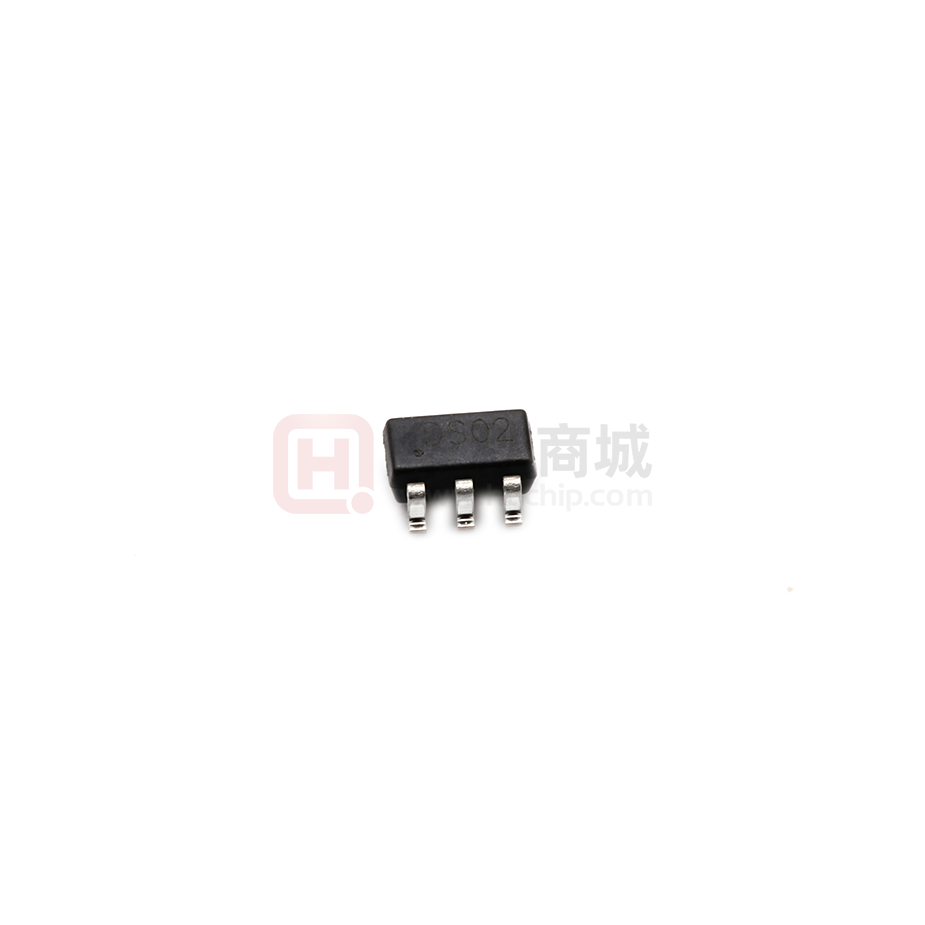
Marking Code: DS02
Schematic Diagram
6.Drain1
4.Drain2
1.Gate1
3.Gate2
5.Source1
2.Source2
Absolute Maximum Ratings
Ratings at TA = 25℃ unless otherwise specified.
Symbol
Rating
Unit
Drain-Source Voltage
VDS
20
V
Gate-Source Voltage
VGS
±12
V
Drain Current-Continuous
ID
2
A
Drain Current-Plused Note1
IDM
10
A
Maximum Power Dissipation
PD
1
W
TJ,TSTG
-55 To 150
℃
Parameter
Operating Junction and Storage Temperature Range
Thermal Characteristics
Parameter
Thermal Resistance,Junction-to-Ambient Note2
www.pingjingsemi.com
Revision:1.0 Apr-2020
Symbol
Max.
Unit
RθJA
125
℃/W
1/5
�PJM4602DNSG-S
Dual N-Channel MOSFET
Electrical Characteristics
TA =25℃ unless otherwise specified.
Parameter
Symbol
Condition
Min
Typ
Max
Unit
Drain-Source Breakdown Voltage
V(BR)DSS
VGS=0V ID=250μA
20
-
-
V
Zero Gate Voltage Drain Current
IDSS
VDS=20V,VGS=0V
-
-
1
μA
Gate-Body Leakage Current
IGSS
VGS=±12V,VDS=0V
-
-
±100
nA
Gate Threshold Voltage
VGS(th)
VDS=VGS,ID=250μA
0.4
0.8
1.2
V
Drain-Source On-State Resistance Note3
RDS(ON)
-
60
80
mΩ
VGS=4.5V, ID=2A
-
48
60
mΩ
VDS=5V,ID=2A
-
5
-
S
-
260
-
pF
-
48
-
pF
Static Characteristics
Forward Transconductance Note3
VGS=2.5V, ID=1A
gFS
Dynamic Characteristics
Input Capacitance
Clss
VDS=10V,VGS=0V,
Output Capacitance
Coss
Reverse Transfer Capacitance
Crss
-
27
-
pF
Turn-on Delay Time
td(on)
-
2.5
-
nS
Turn-on Rise Time
tr
-
3.2
-
nS
-
21
-
nS
f=1.0MHz
Switching Characteristics
Turn-Off Delay Time
td(off)
VDD=10V, RL=3.3Ω
VGS=4.5V,RGEN=6Ω
Turn-Off Fall Time
tf
-
3
-
nS
Total Gate Charge
Qg
-
2.9
5
nC
Gate-Source Charge
Qgs
-
0.4
-
nC
Gate-Drain Charge
Qgd
-
0.6
-
nC
-
-
1.2
V
-
-
2
A
VDS=10V,ID=2A,
VGS=4.5V
Drain-Source Diode Characteristics
Diode Forward Voltage Note 3
VSD
Diode Forward Current Note 2
IS
VGS=0V,IS=2A
Notes: 1. Repetitive rating: pulsed width limited by maximum junction temperature.
2. Surface Mounted on FR4 Board, t ≤ 10 sec.
3. Pulse width ≤ 300μs, duty cycle ≤ 2%
www.pingjingsemi.com
Revision:1.0 Apr-2020
2/5
�PJM4602DNSG-S
Dual N-Channel MOSFET
ID- Drain Current (A)
Rdson On-Resistance(mΩ)
Electrical Characteristics Curves
ID- Drain Current (A)
VDS Drain-Source Voltage (V)
Figure 2 Drain-Source On-Resistance
ID- Drain Current (A)
Normalized On-Resistance
Figure 1 Output Characteristics
Vgs Gate-Source Voltage (V)
TJ-Junction Temperature(℃)
Figure 3 Transfer Characteristics
Figure 4 Drain-Source On-Resistance
C Capacitance (pF)
Rdson On-Resistance(mΩ)
ID=2A
VGS Gate-Source Voltage (V)
Figure 5 RDS(on) vs VGS
www.pingjingsemi.com
Revision:1.0 Apr-2020
VDS Drain-Source Voltage (V)
Figure 6 Capacitance vs VDS
3/5
�VDS=10V
ID=2A
Is- Reverse Drain Current (A)
Vgs Gate-Source Voltage (V)
PJM4602DNSG-S
Dual N-Channel MOSFET
Qg Gate Charge (nC)
VSD Source-Drain Voltage (V)
Figure 7 Gate Charge
ID- Drain Current (A)
Figure 8 Source- Drain Diode Forward
VDS Drain-Source Voltage (V)
r(t),Normalized Effective
Transient Thermal Impedance
Figure 9 Safe Operation Area
Square Wave Pluse Duration(sec)
Figure 10 Normalized Maximum Transient Thermal Impedance
www.pingjingsemi.com
Revision:1.0 Apr-2020
4/5
�PJM4602DNSG-S
Dual N-Channel MOSFET
Package Outline
SOT-23-6
Dimensions in mm
2.92
±0.05
0.15 ±0.02
10
1.6
2.8
±0.1
±0.05
1.9
12
R0.15MAX
0.95
0.35
R0.15MAX
0.06
12
± 0.05
0.65
± 0.03
1.1
±0.05
10
Ordering Information
Device
PJM4602DNSG-S
www.pingjingsemi.com
Revision:1.0 Apr-2020
Package
SOT-23-6
Shipping
3000/Reel&Tape(7inch)
5/5
�
很抱歉,暂时无法提供与“PJM4602DNSG-S”相匹配的价格&库存,您可以联系我们找货
免费人工找货- 国内价格
- 10+0.44723
- 100+0.36170
- 300+0.31893
- 3000+0.24797
- 6000+0.22227
- 9000+0.20942