PJM3400NSQ
N- Enhancement Mode Field Effect Transistor
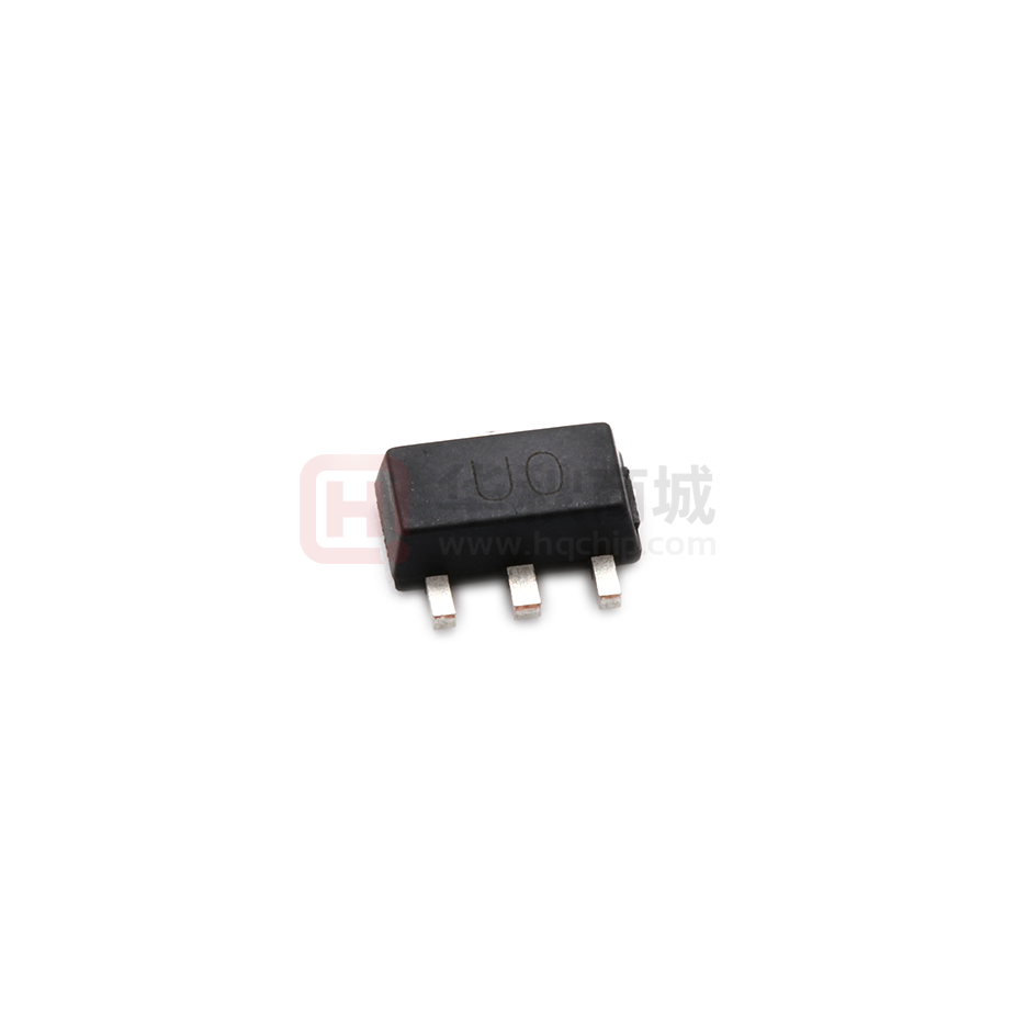
SOT-89
Features
VDS = 30V,ID = 6A
RDS(ON) < 45mΩ @ VGS=2.5V
RDS(ON) < 31mΩ @ VGS=4.5V
RDS(ON) < 27mΩ @ VGS=10V
High power and current handing capability
1. Gate
2.Drain
3.Source
Marking: U0
Applications
Load switch and in PWM applications
Power management
Schematic diagram
3Drain
1
Gate
2 Source
Absolute Maximum Ratings
Ratings at 25℃ ambient temperature unless otherwise specified.
Parameter
Symbol
Limit
Unit
Drain-Source Voltage
VDS
30
V
Gate-Source Voltage
VGS
±12
V
Drain Current-Continuous
ID
6
A
Drain Current-Pulsed Note1
IDM
30
A
Maximum Power Dissipation
PD
1.4
W
TJ,TSTG
150,-55 To 150
℃
RθJA
89
℃/W
Operating Junction and Storage Temperature Range
Thermal Characteristics
Thermal Resistance,Junction-to-Ambient Note2
www.pingjingsemi.com
Revision:1.0 May-2019
1/5
�PJM3400NSQ
N- Enhancement Mode Field Effect Transistor
Electrical Characteristics
(TA=25℃ unless otherwise noted)
Parameter
Symbol
Condition
Min
Typ
Max
Unit
Drain-Source Breakdown Voltage
V(BR)DSS
VGS=0V ID=250μA
30
-
-
V
Zero Gate Voltage Drain Current
IDSS
VDS=30V,VGS=0V
-
-
1
μA
Gate-Body Leakage Current
IGSS
VGS=±12V,VDS=0V
-
-
±100
nA
VGS(th)
VDS=VGS,ID=250μA
0.7
0.9
1.4
V
VGS=2.5V, ID=4A
-
-
45
mΩ
VGS=4.5V, ID=5A
-
-
31
mΩ
VGS=10V, ID=5.8A
-
-
27
mΩ
VDS=5V,ID=5A
10
-
-
S
-
825
-
pF
-
100
-
pF
-
78
-
pF
-
3.3
-
nS
-
4.8
-
nS
-
26
-
nS
-
4
-
nS
-
10
-
nC
-
1.6
-
nC
-
3.1
-
nC
-
-
1.2
V
-
-
5.8
A
Static Characteristics
Gate Threshold
Voltage Note3
Drain-Source On-State Resistance Note3
Forward
Transconductance Note3
RDS(ON)
gFS
Dynamic Characteristics
Input Capacitance
Ciss
Output Capacitance
Coss
Reverse Transfer Capacitance
Crss
VDS=15V,VGS=0V,
f=1.0MHz
Switching Characteristics
Turn-on Delay Time
td(on)
Turn-on Rise Time
tr
Turn-Off Delay Time
td(off)
Turn-Off Fall Time
tf
Total Gate Charge
Qg
Gate-Source Charge
Qgs
Gate-Drain Charge
Qgd
VDD=15V, RL=2.7Ω
VGS=10V,RGEN=3Ω
VDS=15V,ID=5.8A,
VGS=4.5V
Drain-Source Diode Characteristics
Diode Forward Voltage Note3
Diode Forward Current
Note2
VSD
VGS=0V,IS=5.8A
IS
Notes:
1.
2.
3.
Repetitive Rating: Pulse width limited by maximum junction temperature.
Surface Mounted on FR4 Board, t ≤ 10 sec.
Pulse Test: Pulse Width ≤ 300μs, Duty Cycle ≤ 2%.
www.pingjingsemi.com
Revision:1.0 May-2019
2/5
�PJM3400NSQ
N- Enhancement Mode Field Effect Transistor
PD Power(W)
ID- Drain Current (A)
Typical Characteristics Curves
TJ-Junction Temperature(℃)
TJ-Junction Temperature(℃)
Drain Current
ID- Drain Current (A)
Rdson On-Resistance(Ω)
Power Dissipation
ID- Drain Current (A)
Vds Drain-Source Voltage (V)
Drain-Source On-Resistance
ID- Drain Current (A)
Normalized On-Resistance
Output Characteristics
Vgs Gate-Source Voltage (V)
TJ-Junction Temperature(℃)
Transfer Characteristics
Drain-Source On-Resistance
www.pingjingsemi.com
Revision:1.0 May-2019
3/5
�C Capacitance (pF)
Rdson On-Resistance(Ω)
PJM3400NSQ
N- Enhancement Mode Field Effect Transistor
Vds Drain-Source Voltage (V)
Rdson vs Vgs
Capacitance vs Vds
Vgs Gate-Source Voltage (V)
Is- Reverse Drain Current (A)
Vgs Gate-Source Voltage (V)
Qg Gate Charge (nC)
Vsd Source-Drain Voltage (V)
Gate Charge
Source- Drain Diode Forward
www.pingjingsemi.com
Revision:1.0 May-2019
4/5
�PJM3400NSQ
N- Enhancement Mode Field Effect Transistor
Package Outline
SOT-89
Ordering Information
Device
PJM3400NSQ
www.pingjingsemi.com
Revision:1.0 May-2019
Package
SOT-89
Shipping
1000/Reel&Tape(7inch)
5/5
�
很抱歉,暂时无法提供与“PJM3400NSQ”相匹配的价格&库存,您可以联系我们找货
免费人工找货- 国内价格
- 10+0.47013
- 100+0.37163
- 300+0.32238