PJM2307PSA
P- Enhancement Mode Field Effect Transistor
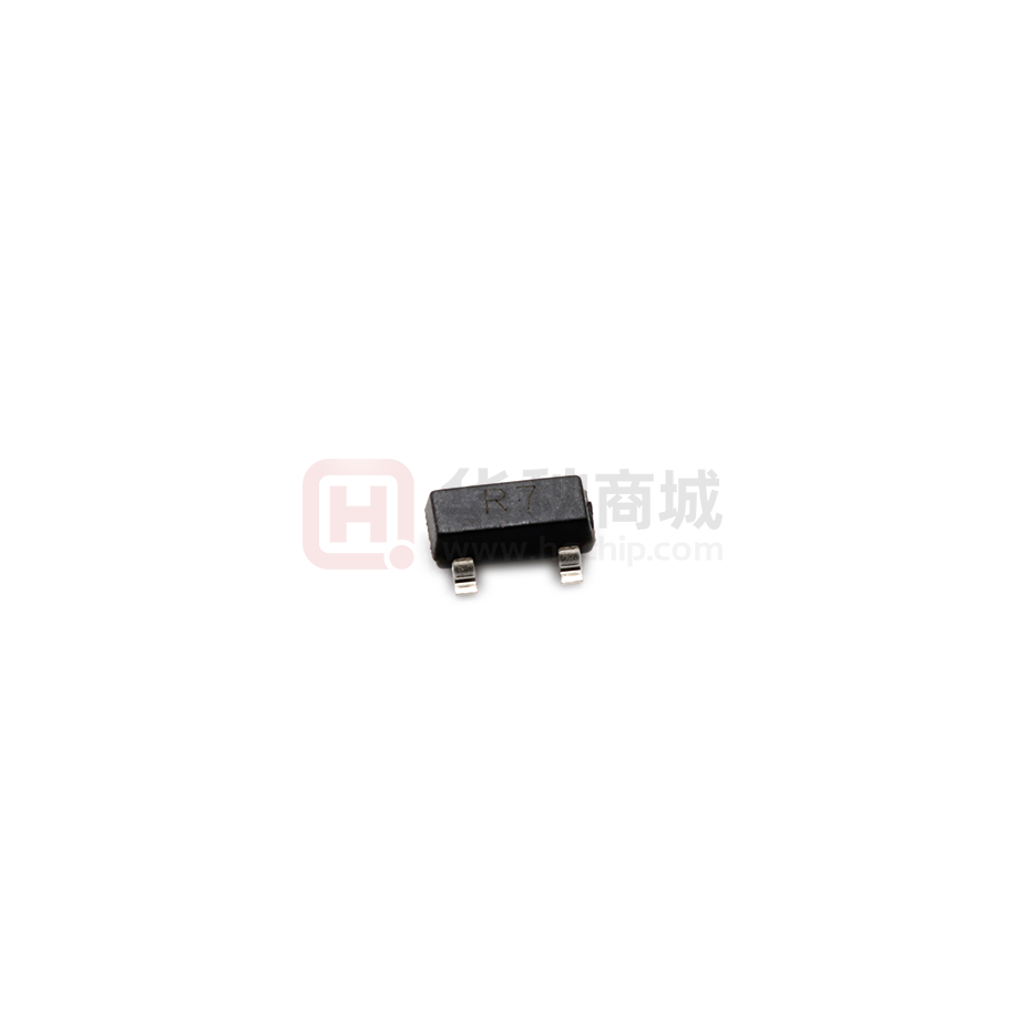
SOT-23
Features
VDS = -30V,ID = -2.7A
RDS(ON) = 110mΩ (Typ.) @ VGS=-4.5V
RDS(ON) = 73mΩ (Typ.) @ VGS=-10V
Low gate charge and RDS(ON)
Low reverse transfer capacitances
1. Gate
2.Source
3.Drain
Marking: R7
Schematic Diagram
Application
Load switch and in PWM applicatopns
Power management
Drain
3
1
Gate
2 Source
Absolute Maximum Ratings
Ratings at TC =25℃ unless otherwise specified.
Symbol
Value
Units
Drain-Source Voltage
Parameter
-VDS
30
V
Gate-Source Voltage
VGS
±20
V
Continuous Drain Current
-ID
2.7
A
Power Dissipation
PD
0.9
W
150, -55 to 150
°C
Junction and Storage Temperature Range
TJ, TSTG
Thermal Characteristics
Parameter
Symbol
Typ.
Units
Maximum Junction-to-Ambient Note1
RθJA
139
°C/W
www.pingjingsemi.com
Revision:1.1 Jun-2019
1/6
�PJM2307PSA
P- Enhancement Mode Field Effect Transistor
Electrical Characteristics
TA=25℃ unless otherwise noted
Parameter
Symbol
Test Condition
Min
Typ
Max
Unit
Static Characteristics
-V(BR)DSS
VGS = 0V, ID =-250µA
Gate-Source Leakage
IGSS
VDS =0V, VGS =±20V
±100
nA
Zero Gate Voltage Drain Current
-IDSS
VDS =-30V, VGS =0V
1
µA
3
V
Drain-Source Breakdown Voltage
Gate threshold voltage Note2
-VGS(th)
Drain-Source On-State Resistance Note2
RDS(on)
Forward Transconductance Note2
gfs
VDS =VGS, ID = -250µA
30
V
1
VGS =-4.5V, ID =-2.5A
110
138
VGS =-10V, ID =-3.5A
73
88
VDS =-10V, ID =-3.5A
7
mΩ
S
Dynamic Characteristics
Input Capacitance
Ciss
Output Capacitance
Coss
Reverse Transfer Capacitance
Crss
340
VDS =-15V,VGS =0V,f =1MHz
pF
67
51
Switching Characteristics
Total Gate Charge
Qg
Gate-Source Charge
Qgs
Gate-Drain Charge
Qgd
Turn-On Delay Time
td(on)
Rise Time
Turn-Off Delay Time
Fall Time
tr
td(off)
VDS =-15V,VGS =-4.5V,
ID =-2.5A
4.1
6.2
nC
1.3
1.8
VDD=-15V,
RL=15Ω, ID =-1A,
VGEN=-4.5V,Rg=1Ω
tf
40
60
40
60
20
40
17
30
0.8
1.2
ns
Source-Drain Diode characteristics
Body Diode Voltage
-VSD
IS=-0.75A, ,VGS =0
V
Notes:
1. Surface mounted on FR4 board,t ≤ 10 sec.
2. Pulse Test :pulse width < 300µs, duty cycle ≤2%.
www.pingjingsemi.com
Revision:1.1 Jun-2019
2/6
�PJM2307PSA
P- Enhancement Mode Field Effect Transistor
Typical Characteristics Curves
Output Characteristics
-20
Pulsed
Ta=25℃
Pulsed
VGS=-4.5V
(A)
-8
(A)
-16
ID
ID
VGS=-4.0V
-6
VGS=-3.5V
-8
VGS=-3.0V
DRAIN CURRENT
DRAIN CURRENT
-12
-4
-0
-0
-1
-2
-3
-4
DRAIN TO SOURCE VOLTAGE
RDS(ON) ——
VDS
-5
-0
-1
-2
-3
GATE TO SOURCE VOLTAGE
(V)
ID
RDS(ON) ——
500
-4
VGS
-5
(V)
VGS
Ta=25℃
Ta=25℃
Pulsed
Pulsed
400
RDS(ON)
(m)
250
200
ON-RESISTANCE
(m)
300
RDS(ON)
-4
-2
-0
ON-RESISTANCE
Transfer Characteristics
-10
VGS=-10V,-8V,-6V
Ta=25℃
VGS=-4.5V
150
VGS=-10V
100
300
ID=-3.5A
200
100
50
0
-0
-4
-8
DRAIN CURRENT
-12
ID
-16
-20
(A)
-0
-4
-8
-12
GATE TO SOURCE VOLTAGE
-16
VGS
-20
(V)
IS —— VSD
-10
Ta=25℃
SOURCE CURRENT
IS (A)
Pulsed
-1
-0.1
-0.01
-0.0
-0.3
-0.6
-0.9
SOURCE TO DRAIN VOLTAGE
www.pingjingsemi.com
Revision:1.1 Jun-2019
-1.2
-1.5
VSD (V)
3/6
�PJM2307PSA
P- Enhancement Mode Field Effect Transistor
Package Outline
SOT-23
0.8
Max.
1.025
1.150
A1
0.000
0.050
0.100
b
c
D
0.300
0.080
2.800
0.400
0.115
2.900
0.500
0.150
3.000
E
1.200
1.300
1.400
HE
2.250
2.400
2.550
e
1.800
1.900
2.000
0.550REF
L1
L
0.300
0o
θ
0.500
8o
2.2
Typ.
0.900
0.8
1.0
Min.
A
1.0
Dimensions in millimeter
Symbol
1.9
SOT-23 (TO-236)
Recommended Soldering Pad
Ordering Information
Device
PJM2307PSA
www.pingjingsemi.com
Revision:1.1 Jun-2019
Package
SOT-23
Shipping
3000/Reel&Tape(7inch)
4/6
�PJM2307PSA
P- Enhancement Mode Field Effect Transistor
Conditions of Soldering and Storage
Recommended condition of reflow soldering
Figure
Recommended peak temperature is over 245℃. If peak temperature is below 245℃, you may adjust
the following parameters:
Time length of peak temperature (longer)
Time length of soldering (longer)
Thickness of solder paste (thicker)
Conditions of hand soldering
Temperature: 370 ℃
Time: 3s max.
Times: one time
Storage conditions
Temperature
5 to 40 ℃
Humidity
30 to 80% RH
Recommended period
One year after manufacturing
www.pingjingsemi.com
Revision:1.1 Jun-2019
5/6
�PJM2307PSA
P- Enhancement Mode Field Effect Transistor
Package Specifications
The method of packaging
Cover Tape
SOT-23
3,000 pcs per reel
1
3
2
Carrier Tape
30,000 pcs per box
10 reels per box
220
195
0
435
21
43
5
120,000 pcs per carton
4 boxes per carton
210
Embossed tape and reel data
D
A
T2
T1
4.0
4.0
B
8.0
C
E
1Pin
G
N
Tape (8mm)
F
Reel (7'')
www.pingjingsemi.com
Revision:1.1 Jun-2019
Symbol
A
B
C
E
F
D
T1
T2
N
G
Value (unit: mm)
Ø 177.8±1
2.7±0.2
Ø 13.5±0.2
Ø 54.5±0.2
12.3±0.3
9.6+2/-0.3
1.0±0.2
1.2±0.2
3.15±0.1
1.25±0.1
6/6
�
很抱歉,暂时无法提供与“PJM2307PSA”相匹配的价格&库存,您可以联系我们找货
免费人工找货- 国内价格
- 10+0.34647
- 100+0.27389
- 300+0.23760