PJM123NSA
N- Enhancement Mode Field Effect Transistor
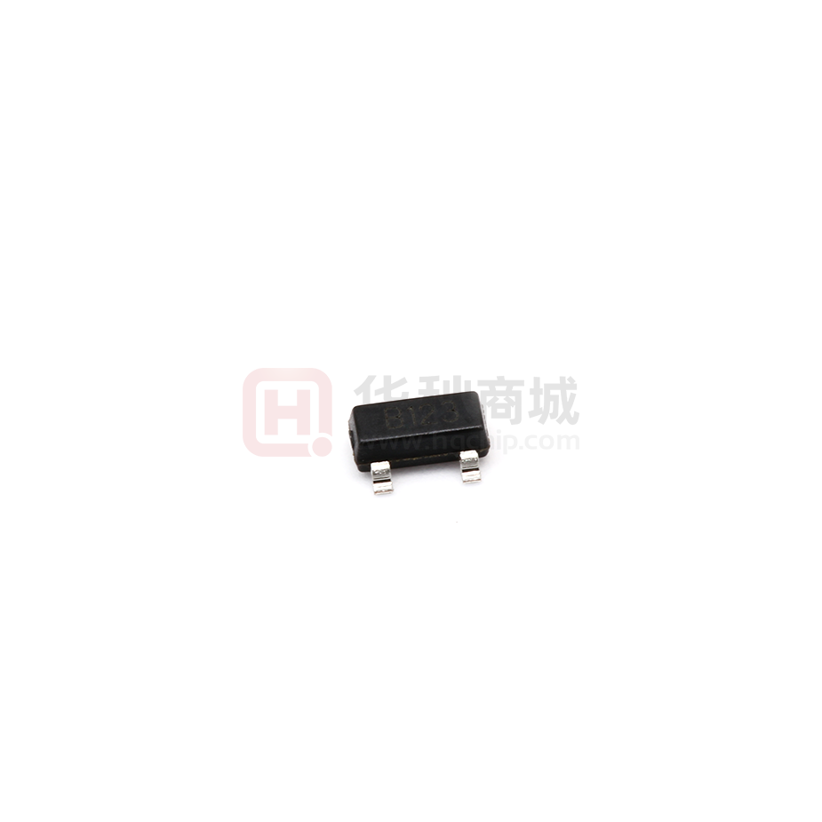
SOT-23
Features
◆
Surface Mount Package
◆
Low RDS(ON)
◆
ESD protected(HBM) up to 2KV
1. Gate
2.Source 3.Drain
Marking: B123
Applications
◆
Switching Application
◆
Small Servo Motor Controls
Schematic diagram
D
G
S
Absolute Maximum Ratings
(TC=25℃, unless otherwise noted)
Parameter
Symbol
Value
Unit
Drain-Source Voltage
VDS
100
V
Gate-Source Voltage
VGS
±20
V
ID
0.17
IDM
0.68
Power Dissipation
PD
0.9
W
Junction Temperature
TJ
150
°C
TSTG
-55 to 150
°C
Symbol
Typ.
Units
RθJA
139
°C/W
Continuous Drain Current
Pulsed Drain Current
tp=10μs
Storage Temperature Range
A
Thermal Characteristics
Parameter
Maximum Junction-to-Ambient Note1
www.pingjingsemi.com
Revision:1.1 Jan-2019
1/6
�PJM123NSA
N- Enhancement Mode Field Effect Transistor
Electrical Characteristics
(TA=25℃, unless otherwise noted)
Parameter
Symbol
Test Conditions
Min
Typ
Max
Unit
100
-
-
V
Static Parameters
Drain-Source Breakdown Voltage
V(BR)DSS VGS = 0V, ID = 250μA
Gate Leakage Current
IGSS
VDS = 0V, VGS = ±20V
-
-
±10
μA
Zero Gate Voltage Drain Current
IDSS
VDS =100V, VGS = 0V
-
-
1
μA
VGS(th)
VDS = VGS, ID = 250μA
1
-
3
V
VGS = 10V, ID =0.17A
-
3.5
6
Ω
VGS = 4.5V, ID =0.17A
-
3.8
10
Ω
VDS = 10V, ID = 0.17A
80
-
-
mS
-
29
60
-
10
15
-
2
6
-
-
8
-
-
8
Gate Threshold Voltage Note2
Drain-Source On-Resistance
Note2
Forward transconductance Note2
RDS(ON)
gfs
Dynamic Parameters
Input Capacitance
Ciss
Output Capacitance
Coss
Reverse Transfer Capacitance
Crss
VDS = 25V,
VGS = 0V,
f = 1MHz
pF
Switching Parameters
Turn-On Delay Time
td(on)
Turn-On Rise Time
tr
Turn-Off Delay Time
td(off)
-
-
13
Turn-Off Fall Time
tf
-
-
16
Total Gate Charge
Qg
-
1.4
2
Gate-Source Charge
Qgs
-
0.15
0.25
Gate-Drain Charge
Qgd
-
0.2
0.4
IS
-
-
0.17
A
-
-
1.3
V
VDD=30V, VGS=10V
RGEN=50Ω, ID=0.28A
VDS=10V,VGS=10V,ID=0.22A
ns
nC
Drain-source Diode Parameters
Source-Drain Diode Current
Forward Diode Voltage
VSD
VGS = 0V, IS = 0.34A
Notes:1. Surface mounted on FR4 board using the minimum recommended pad size.
2. Pulse Test: Pulse width=300μs, duty cycle≤2%.
www.pingjingsemi.com
Revision:1.1 Jan-2019
2/6
�PJM123NSA
N- Enhancement Mode Field Effect Transistor
Ratings And Characteristic Curves
Output Characteristics
Transfer Characteristics
450
450
Ta=25℃
VGS=4V,5V,6V
400
Pulsed
VGS=3V
Pulsed
(mA)
350
300
ID
300
VGS=2.5V
250
DRAIN CURRENT
ID
(mA)
350
DRAIN CURRENT
VDS=3V
400
200
150
100
Ta=100℃
200
150
100
VGS=2V
50
0
0.0
Ta=25℃
250
50
0.5
1.0
1.5
2.0
2.5
3.0
3.5
DRAIN TO SOURCE VOLTAGE
VDS
4.0
4.5
0
0.0
5.0
0.5
1.0
(V)
1.5
2.0
2.5
3.0
GATE TO SOURCE VOLTAGE
VGS
3.5
RDS(ON) —— VGS
RDS(ON) —— ID
6
30
Pulsed
Ta=25℃
ID=0.17A
25
RDS(ON)
( )
5
RDS(ON)
VGS=4.5V
ON-RESISTANCE
( )
Pulsed
ON-RESISTANCE
4.0
(V)
4
VGS=10V
3
20
15
10
Ta=100℃
5
Ta=25℃
2
50
100
150
200
DRAIN CURRENT
250
D
300
0
350
0
(mA)
1
2
3
4
5
6
7
GATE TO SOURCE VOLTAGE
GS
8
9
10
(V)
Threshold Voltage
IS —— VSD
400
2.0
1.8
VTH
Ta=25℃
Ta=100℃
10
0.0
0.2
0.4
0.6
0.8
SOURCE TO DRAIN VOLTA
VOLTAGE
www.pingjingsemi.com
Revision:1.1 Jan-2019
THRESHOLD VOLTAGE
100
SOURCE CURRENT
IS (mA)
(V)
Pulsed
1.0
SD
1.2
(V)
1.4
1.6
ID=250uA
1.4
1.2
1.0
25
50
75
JUNCTION TEMPERATURE
100
Tj
125
(℃ )
3/6
�PJM123NSA
N- Enhancement Mode Field Effect Transistor
Package Outline
SOT-23(TO-236)
0.8
Typ.
Max.
0.900
1.025
1.150
A1
0.000
0.050
0.100
b
c
D
0.300
0.080
2.800
0.400
0.115
2.900
0.500
0.150
3.000
E
1.200
1.300
1.400
HE
2.250
2.400
2.550
e
1.800
1.900
2.000
0.550REF
L1
L
0.300
θ
0°
0.500
8°
2.2
Min.
A
1.0
Dimensions in millimeter
0.8
1.0
Symbol
1.9
SOT-23 (TO-236)
Recommended soldering pad
Ordering Information
Device
PJM123NSA
www.pingjingsemi.com
Revision:1.1 Jan-2019
Package
SOT-23
Shipping
3000/Reel&Tape(7inch)
4/6
�PJM123NSA
N- Enhancement Mode Field Effect Transistor
Conditions of Soldering and Storage
Recommended condition of reflow soldering
Recommended peak temperature is over 245 OC. If peak temperature is below 245 OC, you may adjust
the following parameters:
Time length of peak temperature (longer)
Time length of soldering (longer)
Thickness of solder paste (thicker)
Conditions of hand soldering
Temperature: 370 OC
Time: 3s max.
Times: one time
Storage conditions
Temperature
5 to 40 OC
Humidity
30 to 80% RH
Recommended period
One year after manufacturing
www.pingjingsemi.com
Revision:1.1 Jan-2019
5/6
�PJM123NSA
N- Enhancement Mode Field Effect Transistor
Package Specifications
The method of packaging
Cover Tape
SOT-23 (TO-236)
3,000 pcs per reel
1
3
2
Carrier Tape
30,000 pcs per box
10 reels per box
220
195
0
435
21
43
5
120,000 pcs per carton
4 boxes per carton
210
Embossed tape and reel data
D
A
T2
T1
4.0
4.0
B
8.0
C
E
1Pin
G
N
Tape (8mm)
F
Reel (7'')
www.pingjingsemi.com
Revision:1.1 Jan-2019
Symbol
A
B
C
E
F
D
T1
T2
N
G
Value (unit: mm)
Ø 177.8±1
2.7±0.2
Ø 13.5±0.2
Ø 54.5±0.2
12.3±0.3
9.6+2/-0.3
1.0±0.2
1.2±0.2
3.15±0.1
1.25±0.1
6/6
�
很抱歉,暂时无法提供与“PJM123NSA”相匹配的价格&库存,您可以联系我们找货
免费人工找货- 国内价格
- 20+0.20682
- 200+0.16481
- 600+0.14148
- 3000+0.11070
- 9000+0.09861
- 21000+0.09202
- 国内价格
- 5+1.07270
- 20+0.97805
- 100+0.88340
- 500+0.78875
- 1000+0.74458
- 2000+0.71303