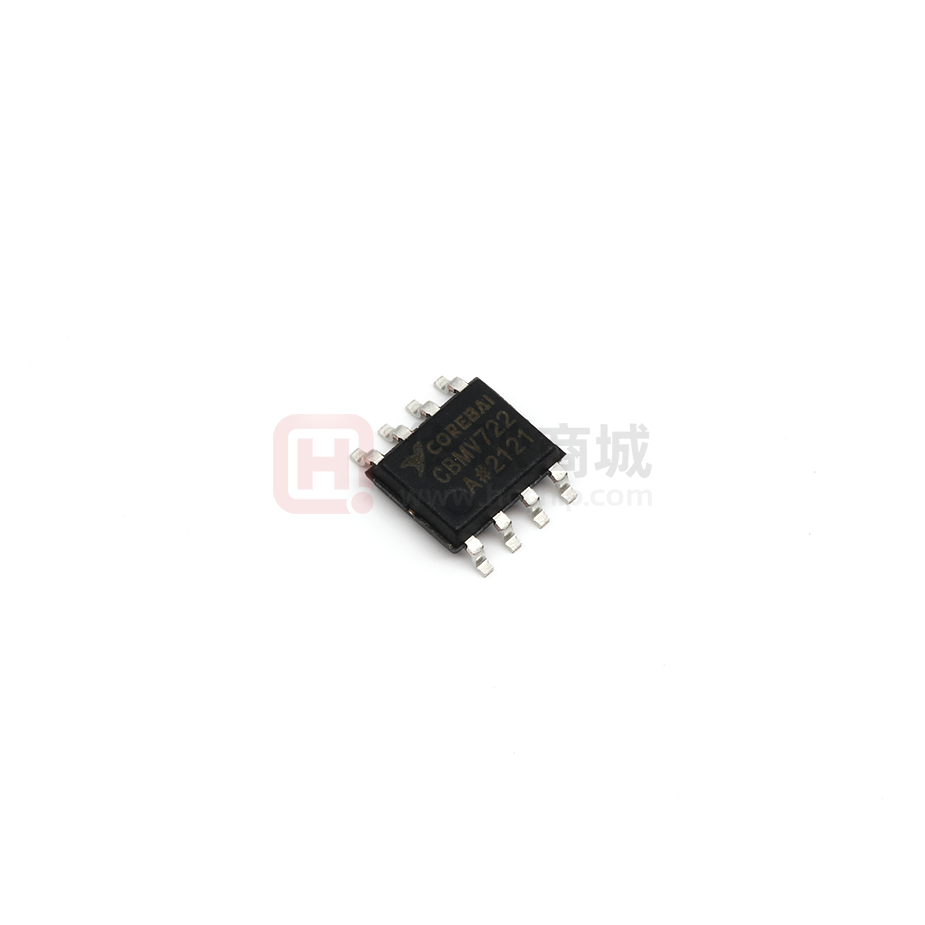
CBMV721S-CBMV722S-CBMV721-CBMV722-CBMV724
OPERATION INSTRUCTION
FEATURES
APPLICATIONS
HIGH GAIN BANDWIDTH:10MHz
SENSORS
RAIL-TO-RAIL INPUT AND OUTPUT
PHOTODIODE AMPLIFICATION
0.9mV Typical Vos
ACTIVE FILTERS
INPUT VOLTAGE RANGE: -0.1V to +5.6V
TEST EQUIPMENT
with Vs = 5.5V
DRIVING A/D CONVERTERS
SUPPLY RANGE: +2.5V to +5.5V
SHUTDOWN: CBMV721S/CBMV722S
SPECIFIED UP TO +125°C
MicroSIZE PACKAGES: SOT23-5, SOT23-6
DESCRIPTION
The CBMV72X families of products offer low voltage operation and rail-to-rail input and
output, as well as excellent speed/power consumption ratio, providing an excellent bandwidth
(10MHz) and slew rate of 7V/us. The op-amps are unity gain stable and feature an ultra-low input
bias current.
The devices are ideal for sensor interfaces, active filters and portable applications. The
CBMV721S, CBMV722S include a shutdown mode. Under logic control, the amplifiers can be
switched from normal operation to a standby current that is less than 1uA.The CBMV72X families
of operational amplifiers are specified at the full temperature range of −40°C to +125°C under
single or dual power supplies of 2.5V to 5.5V.
1
www.corebai.com
�CBMV721S-CBMV722S-CBMV721-CBMV722-CBMV724
OPERATION INSTRUCTION
PIN CONFIGURATIONS
ABSOLUTE MAXIMUM RATINGS (1)
Supply Voltage, V+ to V-........................................7.0V
(1)
Stresses above these ratings may cause
Input Terminals, Voltage (2) .... – 0.5 to (V+) + 0.5V
permanent damage. Exposure to absolute
Current (2)..……..……...…..... ±10mA
maximum conditions for extended periods
Storage Temperature ……….…..… −65°C to +150°C
may degrade device reliability. These are
Operating Temperature ……….… −40°C to +125°C
stress ratings only, and functional operation
Junction Temperature...........................................150°C
of the device at these or any other conditions
Package Thermal Resistance @ TA = +25°C
beyond those specified is not implied.
SOT23-5, SOT23-6………………….………..……200°C/W
(2)
MSOP-10, SOIC-8 ……………..……….…..….... 150°C/W
the power-supply rails. Input signals that can
SOIC-14, TSSOP-14………….……….………...…100°C/W
swing more than 0.5V beyond the supply rails
Lead Temperature (Soldering, 10s) ……….......260°C
should be current-limited to 10mA or less.
Input terminals are diode-clamped to
ESD Susceptibility
HBM ….......................................................................5000V
MM ……………………….........…………………….……….400V
2
www.corebai.com
�CBMV721S-CBMV722S-CBMV721-CBMV722-CBMV724
OPERATION INSTRUCTION
ELECTRICAL CHARACTERISTICS
(At TA = +25℃, Vs=5V, RL = 10kΩ connected to VS/2, and VOUT = VS/2, unless otherwise noted.)
CBMV721S,CBMV722S,
PARAMETER
CONDITIONS
TJ
CBMV721,CBMV722,
CBMV724
MIN
TYP
UNIT
MAX
POWER SUPPLY
Vs
IQ
PSRR
Operating Voltage Range
25℃
Quiescent
2.5
25℃
Current/Amplifier
1.15
Power-Supply Rejection
Vs=2.5V to 5.5V,
25℃
75
Ratio
Vcm=(V-)+0.5V
-40℃ to
125℃
65
5.5
V
1.4
mA
85
dB
INPUT
VOS
Input Offset Voltage
VOS TC
Input Offset Voltage
Average Drift
25℃
-40℃ to 125℃
0.5
2.5
2.6
mV
uV/℃
IB
Input Bias Current
25℃
1
10
pA
Ios
Input Offset Current
25℃
1
10
pA
3
www.corebai.com
�CBMV721S-CBMV722S-CBMV721-CBMV722-CBMV724
OPERATION INSTRUCTION
Vcm
CMRR
Common-Mode Voltage
Range
Common-Mode Rejection
Ratio
Vs= 5.5V
25℃
-0.1
Vs= 5.5V,
25℃
73
-40℃ to
125℃
67
25℃
60
Vcm=-0.1V to 5.6V
-40℃ to
125℃
57
RL=2KΩ, Vo=0.15V
25℃
86
-40℃ to
125℃
65
25℃
90
-40℃ to
125℃
66
Vcm=-0.1V to 4V
Vs= 5.5V,
5.6
V
85
dB
75
OUTPUT
to 4.85V
AOL
Open-Loop Voltage Gain
RL=10KΩ,Vo=0.05V
to 4.95V
Output Swing From Rail
Iout
RL=2KΩ
dB
Output Short-Circuit
Current
96
52
25℃
RL=10KΩ
95
mV
7
25℃
70
mA
FREQUENCY RESPONSE
SR
Slew Rate
25℃
7
V/us
GBP
Gain-Bandwidth Product
25℃
10
MHz
PM
Phase Margin
25℃
62
°
ts
Setting Time,0.1%
0.2
us
0.35
us
Overload Recovery Time
VIN·Gain≥VS
NOISE
f=1 KHz
25℃
9.5
nV/√Hz
f=10KHz
25℃
6.5
nV/√Hz
25℃
很抱歉,暂时无法提供与“CBMV722AS8”相匹配的价格&库存,您可以联系我们找货
免费人工找货- 国内价格
- 1+3.38000
- 10+3.12000
- 30+3.06800
