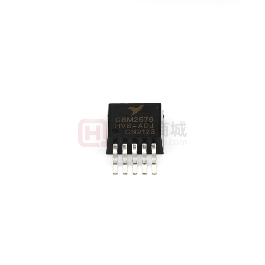
CBM2576HVS-3.3/5.0/12/ADJ
OPERATION INSTRUCTION
FEATURES
APPLICATIONS
3.3 V, 5.0 V, 12 V, and Adjustable Output
Versions
Adjustable version output voltage range,
1.23V
to 57V 土 4% max over line and load
conditions
Output load current: 3A
Input voltage range up to 60V
Requires only 4 external components
52 kHz fixed frequency internal oscillator
TTL shutdown capability, low power
standby mode
High efficiency
Thermal shutdown and current limit
protection
Built-in switching transistor on chip
5-lead T0-220 package
Simple High-Efficiency Step-Down (Buck)
Regulator
Efficient
Pre-Regulator
for
Linear
Regulators
On-Ca「d Switching Regulators
Positive
to
Negative
Converter
(Buck-Boost)
Negative Step-Up Converters
Power Supply for Battery Chargers
GENERAL DESCRIPTION
The CBM2576HVSseries of regulators are monolithic integrated circuits that provide all the
active functions for a step-down (buck) switching regulator, capable of driving 3A load with
excellent line and load regulation. These devices are available in fixed output voltages of 3.3V,
5.0V, 12V, and adjustable output version. Requiring a minimum number of external components,
these regulators are simple to use and include internal frequency compensation and a
fixedfrequency oscillator.
The CBM2576HVSseries offers a high-efficiency replacement for popular three-terminal
linear regulators. It substantially reduces the size of the heat sink, and in some cases no heat sink
is required. A standard series of inductors optimized for use with the CBM2576HVSare available
from several different manufacturers. This feature greatly simplifies the design of switch-mode
power supplies.
Other features include a guaranteed 士 4% tolerance on output voltage within specified input
voltages and output load conditions, and 士 10% on the oscillator frequency. The external
shutdown function can be controlled by logic level and then come into standby mode. The
output switch includes cycle-by-cycle current limiting, as well as thermal shutdown for full
protection under fault conditions.
The CBM2576HVSseries a「e available in a standard 5-lead T0-220 package.
1
www.corebai.com
�CBM2576HVS-3.3/5.0/12/ADJ
OPERATION INSTRUCTION
Block diagram
Figure 1.
3.3V R2 = 2.02k
5.0V, R2 = 3.69k
12V, R2 = 10.56k
For adjustable version
R1 = Open, R2 = on
Typical Electrical Parameters
Parameter, unit
Efficiency,%
Typ. value
Test condition
CBM2576HVS-ADJ
77
VIN = 12V, ILOAD = 3A, VOUT = 5V
CBM2576HVS-3.3
75
CBM2576HVS-5.0
77
CBM2576HVS-12
88
VIN = 15V, ILOAD = 3A
98
VFB = 0V
Max. Duty Cycle {ON), %
Symbol
DCmax
VIN = 12V, ILOAD = 3A
2
www.corebai.com
�CBM2576HVS-3.3/5.0/12/ADJ
OPERATION INSTRUCTION
Typical Application (Fixed Output voltage versions)
Figure 2.
C1—aluminum electrolytic capacitor(100uF, 75V);
C2—aluminum electrolytic capacitor(1000uF, 25V);
L1—inductor (100uH);
D1—Schottky diode
Adjustable Output Voltage Versions
Figure 3.
弈
=
th
=
弈
th
Where Vref = 1.23 V, R1 between 1.0 k and 5.0 k
C1 = 10 nF
C2 = 1 nF
3
www.corebai.com
�CBM2576HVS-3.3/5.0/12/ADJ
OPERATION INSTRUCTION
ABSOLUTE MAXIMUM RATINGS
(Absolute Maximum Ratings indicate limits beyond which damage to the device may occur.)
Rating
Maximum Supply Voltaqe
Symbol
Vin
Value
Unit
63
V
ON/OFF Pin Input Voltage
-0.3V ≤ V ≤ +25
V
Output Voltaoe to Ground (Steadv-State)
-0.1
V
Power Dissipation
TO-220,5-Lead
PD
Internally Limited
W
Thermal Resistance, Junction-to-Ambient
RθJA
65
℃/W
Thermal Resistance, Junction-to-Case
RθJC
5.0
℃/W
T0-263, 5-Lead (D2PAK)
PD
Internally Limited
W
Thermal Resistance, Junction-to-Ambient
RθJA
70
℃/W
Thermal Resistance, Junction-to-Case
RθJC
5.0
℃/W
Storage Temperature Range
Tstg
℃
Minimum ESD Rating (Human Body Model:
2.0
kV
260
℃
150
℃
C=100pF,R=1.5kΩ)
Lead Temperature (Soldering, 10 seconds)
Maximum Junction Temperature
TJ
* Stresses beyond those listed under "absolute maximum ratings" may cause permanent damage
to the device These are stress ratings only and functional operation of the device at these or any
other conditions beyond those indicated under "recommended operating conditions" is not
implied.
Exposure to absolute-maximum-rated conditions for extended periods may affect device
reliability.
OPERATING RATINGS
(Operating Ratings indicate conditions for which the device is intended to be functional, but do
not guarantee specific performance limits. For guaranteed specifications and test conditions, see
the Electrical Characteristics.)
Rating
Symbol
Value
Unit
Operating Junction Temperature Range
TJ
-40 to +125
℃
Supply Voltage
VIN
60
V
4
www.corebai.com
�CBM2576HVS-3.3/5.0/12/ADJ
OPERATION INSTRUCTION
ELECTRICAL CHARACTERISTICS
(Unless otherwise specified, Vin = 12V for the 3.3V, 5.0V, and Adjustable version, Vin = 25V for
the 12V version, and Vin = 30V for the 15V version. ILoad = 500mA, TJ = 25℃, for min/max values
TJ is the operating junction temperature range that applies unless otherwise noted)
IC
CBM2576
HVS-ADJ
Parameter, unit
Symbol
Feedback bias current, nA
IB
Oscillator frequency, kHz
fOSC
Saturation voltage, V
VSAT
Current limit, A
ICL
min
47
42
-
Limit
max
100
500
58
63
1.8
2,0
4.2
3.5
6.9
7.5
IL(O)
2
IL(-1)
30
Quiescent current, mA
IQ
10
Standby quiescent current,
uA
ISTBY
200
ON/OFF pin low level input
voltage (switch on), V
ON/OFF pin high level input
voltage (switch off), V
ON/OFF pin high level input
current (switch off}, uA
VIL
IIH
2.2
2.4
30
ON/OFF pin low level input
current (switch on), uA
IIL
10
Feedback voltage, V
VFB
Output leakage current, mA
1.0
0.8
VIH
1.217
1.243
1.193
1.180
1.273
1.286
Test condition
VFB = 1,3V;
VIN= 12V
VIN= 12V
TA,℃
25±10
125*
-40
VFB = OV;
VIN= 12V;
IOUT = 3A
no external circuit
VFB = OV;
VIN= 12V;
3A ≤ IOUT ≤ 8A
no external circuit
VFB = 12V;
VIN= 60V;
VOUT = OV
no external circuit
VFB = 12V;
VIN= 60V;
VOUT =-1V
no external circuit
VFB = 12V;
VIN= 12V
VFB = OV;
VIN= 60V;
VON/OFF =5V
FB = 0V;
N = 12V
VFB = 0V;
VIN= 12V;
VON/OFF = 5V
VFB = 0V;
VIN= 12V;
VON/OFF= 0V
VIN=12V;ILOAD=0.5A;
VOUT = 5V
8V ≤ VIN ≤ 60V;
0.5A ≤ ILOAD ≤ 3A;
VOUT = 5V
25±10
25士10
125*
-40
25±10
25±10
125*
-40
5
www.corebai.com
�CBM2576HVS-3.3/5.0/12/ADJ
OPERATION INSTRUCTION
Limit
IC
CBM2576
HVS-3.3
Parameter, unit
Symbol
Test condition
min
47
42
max
58
63
1.8
2.0
Oscillator frequency, kHz
fOSC
Saturation voltage, V
VSAT
Current limit, A
ICL
Output leakage current, mA
IL(0)
2
IL(-1)
30
Quiescent current, mA
IQ
10
Standby quiescent current,
uA
lSTBY
200
ON/OFF pin low level input
voltage (switch on), V
ON/OFF pin high level input
voltage (switch off), V
ON/OFF pin high level input
current (switch off), uA
VIL
ON/OFF pin low level input
current (switch on), uA
IIL
-
10
Output voltage, V
VOUT
3.234
3.366
3.168
3.135
3.450
3.682
4.2
3.5
6.9
7.5
1.0
0.8
VIH
2.2
2.4
30
IIH
VIN = 12V
VFB = 0V;
VIN = 12V;
IOUT = 3A
no external circuit
VFB = 0V;
VIN = 12V;
3A ≤ IOUT ≤ 8A;
no external circuit
VFB = 12V;
VIN = 60V;
3A ≤ IOUT ≤ 8A
no external circuit
VFB = 12V;
VIN = 60V;
VOUT = -1V;
no external circuit
VFB = 12V;
VIN = 12V
VFB = 0V;
VIN = 60V;
VON/OFF = 5V
VFB = 0V;
VIN = 12V
VFB = 0V;
VIN = 12V;
VON/OFF = 5V
VFB = 0V;
VIN = 12V;
VON/OFF = 0V
VIN = 12V;
VLOAD=0.5A
6V ≤ VIN ≤ 60V;
0.5A ≤ ILOAD ≤ 3A
TA,℃
25±10
125*
-40
25±10
25±10
125*
-40
25±10
25±10
125*
-40
6
www.corebai.com
�CBM2576HVS-3.3/5.0/12/ADJ
OPERATION INSTRUCTION
IC
CBM2576
HVS-5.0
Parameter, unit
Symbol
Limit
min
max
47
58
42
63
1.8
2.0
Oscillator frequency, kHz
fSOC
Saturation voltage, V
VSAT
Current limit, A
ICL
Output leakage current, mA
IL(0)
2
IL(-1)
30
Quiescent current, mA
IQ
10
Standby quiescent current,
uA
ISTBY
200
ON/OFF pin low level input
voltage (switch on), V
ON/OFF pin high level input
voltage (switch off), V
ON/OFF pin high level input
current (switch off), uA
VIL
IIH
2.2
2.4
30
ON/OFF pin low level input
current (switch on), uA
IIL
10
Output voltage, V
VOUT
4.2
3.5
6.9
7.5
1.0
0.8
VIH
4.90
5.10
4.800
4.750
5.225
5.275
Test condition
VIN = 12V
VFB = 0V;
VIN = 12V;
IOUT = 3A
no external circuit
VFB = 0V;
VIN = 12V;
3A ≤ IOUT ≤ 8A
no external circuit
VFB = 12V;
VIN = 60V;
VOUT = 0A
no external circuit
VFB = 12V;
VIN = 60V;
VOUT = -1A
no external circuit
VFB = 12V;
VIN = 12V
VFB = 0V;
VIN = 60V;
VON/OFF = 5V
VFB = 0V;
VIN = 12V
VFB = 0V;
VIN = 12V;
VON/OFF = 5V
VFB = 0V;
VIN = 12V;
VON/OFF = 0V
VIN = 12V;
ILOAD = 0.5A
8V ≤ VIN ≤ 60V;
0.5A ≤ ILOAD ≤ 3A
TA,℃
25±10
125*
-40
25±10
25±10
125*
-40
25±10
25±10
125*
-40
7
www.corebai.com
�CBM2576HVS-3.3/5.0/12/ADJ
OPERATION INSTRUCTION
IC
CBM2576
HVS-12
Parameter, unit
Symbol
Limit
min
max
47
58
42
63
1.8
2.0
Oscillator frequency, kHz
FOSC
Saturation voltage, V
VSAT
Current limit, A
ICL
Output leakage current, mA
IL(0)
2
IL(-1)
30
Quiescent current, mA
IQ
10
Standby quiescent current,
uA
ON/OFF pin low level input
voltage (switch on), V
ON/OFF pin high level input
voltage (switch off), V
ON/OFF pin high level input
current (switch off), uA
ISTBY
200
IIH
2.2
2.4
30
ON/OFF pin low level input
current (switch on), uA
IIL
10
Output voltage, V
VOUT
VIL
4.2
3.5
6.9
7.5
1.0
0.8
VIH
11.76
12.24
11.52
11.40
12.54
12.66
Test condition
VIN = 25V
VFB = 0V;
VIN = 25V;
IOUT = 3A
no external circuit
VFB = 0V;
VIN = 25V;
3A ≤ IOUT ≤ 8A
no external circuit
VFB = 25V;
VIN = 60V;
VOUT = 0V
no external circuit
VFB = 25V;
VIN = 60V;
VOUT = -1V
no external circuit
VFB = 25V;
VIN = 25V
VFB = 0V; VIN = 60V;
VON/OFF = 5V
VFB = 0V;
VIN = 25V
VFB = 0V;
VIN = 25V;
VON/OFF = 5V
VFB = 0V;
VIN = 25V;
VON/OFF = 0V
VIN = 25V;
ILOAD = 0.5A
15V ≤ VIN ≤ 60V;
0.5A ≤ ILOAD ≤ 3A
TA,℃
25±10
125*
-40
25±10
25±10
125*
-40
25±10
25±10
125*
-40
* Junction temperature. Junction temperature is equal to ambient because of measurements of electric
parameters are executed in pulse mode.
8
www.corebai.com
�CBM2576HVS-3.3/5.0/12/ADJ
OPERATION INSTRUCTION
Application Information
INVERTING REGULATOR
Figure 4 shows a CBM2576-12 in a buck-boost configuration to generate a negative 12V
output from a positive input voltage. This circuit bootstraps the regulator's ground pin to the
negative output voltage, then by grounding the feedback pin, the regulator senses the inverted
output voltage and regulates it to -12V.
For an input voltage of 12V or more, the maximum available output current in this
configuration is approximately 700 mA. At lighter loads, the minimum input voltage required
drops to approximately 4.7V.
The switch currents in this buck-boost configuration are higher than in the standard
buck-mode design, thus lowering the available output current. Also, the start-up input current of
the buck-boost converter is higher than the standard buck-mode regulator, and this may
overload an input power source with a current limit less than 5A. Using a delayed turn-on or an
undervoltage lockout circuit (described in the next section) would allow the input voltage to rise
to a high enough level before the switcher would be allowed to turn on.
Because of the structural differences between the buck and the buck-boost regulator
topologies, the buck regulator design procedure section can not be used to to select the
inductor or the output capacitor. The recommended range of inductor values for the buck-boost
design is between 68µH and 220µH, and the output capacitor values must be larger than what is
normally required for buck designs. Low input voltages or high output currents require a large
value output capacitor (in the thousands of micro Farads).
The peak inductor current, which is the same as the peak switch current, can be calculated
from the following formula:
Ip ≈
ILOAD VIN
VIN
VO
VIN |VO |
×
VIN |VO |
L FOSC
Where fOSC = 52 kHz. Under normal continuous inductor current operating conditions, the
minimum VIN represents the worst case. Select an inductor that is rated for the peak current
anticipated.
9
www.corebai.com
�CBM2576HVS-3.3/5.0/12/ADJ
OPERATION INSTRUCTION
FIGURE 4. Inverting Buck-Boost Develops -12V
Also, the maximum voltage appearing across the regulator is the absolute sum of the input
and output voltage. For a -12V output, the maximum input voltage for the IL2576 is +28V.
NEGATIVE BOOST REGULATOR
Another variation on the buck-boost topology is the negative boost configuration. The
circuit in Figure 5 accepts an input voltage ranging from -SV to -12V and provides a regulated
-12V output. Input voltages greater than-12V will cause the output to rise above -12V, but will
not damage the regulator
Typical Load Current
400 mA for VIN= -5.2V
750 mA for VIN = -7V
Note: Heat sink may be required
FIGURE 5. Negative Boost
10
www.corebai.com
�CBM2576HVS-3.3/5.0/12/ADJ
OPERATION INSTRUCTION
Because of the boosting function of this type of regulator, the switch current is relatively
high, especially at low input voltages.
Output load current limitations are a result of the maximum current rating of the switch. Also,
boost regulators can not provide current limiting load protection in the event of a shorted load,
so some other means (such as a fuse) may be necessary.
UNDERVOLTAGE LOCKOUT
In some applications it is desirable to keep the regulator off until the input voltage reaches a
certain threshold. An undervoltage lockout circuit which accomplishes this task is shown in
Figure 6 while Figure 7 shows the same circuit applied to a buck-boost configuration. These
circuits keep the regulator off until the input voltage reaches a predetermined level.
VTH =VZ1 + 2VBE(Q1)
FIGURE 6. Undervoltage Lockout for Buck Circuit
FIGURE 7. Undervoltage Lockout for Buck-Boost Circuit
11
www.corebai.com
�CBM2576HVS-3.3/5.0/12/ADJ
OPERATION INSTRUCTION
DELAYED STARTUP
The ON /OFF pin can be used to provide a delayed startup feature as shown in Figure 8. With
an input voltage of 20V and for the part values shown, the circuit provides approximately 10 ms
of delay time before the circuit begins switching
Increasing the RC time constant can provide longer delay times. But excessively large RC
time constants can cause problems with input voltages that are high in 60Hz or 120Hz ripple, by
coupling the ripple into the ON /OFF pin.
FIGURE 8. Delayed Startup
ADJUSTABLE OUTPUT, LOW-RIPPLE POWER SUPPLY
A 3A power supply that features an adjustable output voltage is shown in Figure 9. An
additional L-C filter that reduces the output ripple by a factor of 10 or more is included in this
circuit.
FIGURE 9. Adjustable 3A Power Supply with Low Output Ripple
12
www.corebai.com
�CBM2576HVS-3.3/5.0/12/ADJ
OPERATION INSTRUCTION
Definition of Terms
BUCK REGULATOR
A switching regulator topology in which a higher voltage is converted to a lower voltage.
Also known as a step-down switching regulator.
BUCK-BOOST REGULATOR
A switching regulator topology in which a positive voltage is converted to a negative voltage
without a transformer.
DUTY CYCLE (D)
Ratio of the output switch's on-time to the oscillator period.
for buck regulator
D=
tON
=
for buck-boost regulator
D=
tON
=
T
T
VOUT
VIN
|VO |
|VO | VIN
CATCH DIODE OR CURRENT STEERING DIODE
The diode which provides a return path for the load current when the IL2576 switch is OFF.
EFFICIENCY (η)
The proportion of input power actually delivered to the load.
η=
POUT
POUT
≈
PIN
POUT PLOSS
13
www.corebai.com
�CBM2576HVS-3.3/5.0/12/ADJ
OPERATION INSTRUCTION
PACKAGE INFORMATION
TO-220-5L
SYMBOL
DIMENSIONS IN MILLIMETERS
DIMENSIONS IN INCHES
MIN
NOM
MAX
MIN
NOM
MAX
A
4.07
4.45
4.82
0.160
0.175
0.190
b
0.76
0.89
1.02
0.030
0.035
0.040
C
0.36
0.50
0.64
0.014
0.020
0.025
D
14.22
14.86
15.50
0.560
0.585
0.610
E
9.78
10.16
10.54
0..385
0.400
0.415
e
1.57
1.71
1.85
0.062
0.067
0.073
e1
6.68
6.81
6.93
0.263
0.268
0.273
F
1.14
1.27
1.40
0.045
0.050
0.055
H1
5.46
6.16
6.86
0.215
0.243
0.270
J1
2.29
2.74
3.18
0.090
0.108
0.125
L
13.21
13.97
14.73
0.520
0.550
0.580
øp
3.68
3.81
3.94
0.145
0..150
0.155
Q
2.54
2.73
2.92
0.100
0.107
0.115
14
www.corebai.com
�CBM2576HVS-3.3/5.0/12/ADJ
OPERATION INSTRUCTION
TO-263-5L
SYMBOL
DIMENSIONS IN MILLIMETERS
DIMENSIONS IN INCHES
MIN
NOM
MAX
MIN
NOM
MAX
A
4.07
4.46
4.85
0.160
0.176
0.191
B
0.66
0.84
1.02
0.026
0.033
0.040
C
0.36
0.50
0.64
0.014
0.020
0.025
C2
1.14
1.27
1.40
0.045
0.050
0.055
D
8.65
9.15
9.65
0.341
0.360
0.380
E
9.78
10.16
10.54
0.385
0.400
0.415
e
1.57
1.71
1.85
0.062
0.068
0.073
F
6.60
6.86
7.11
0.260
0.270
0.280
L
14.61
15.24
15.88
0.575
0.600
0.625
L1
2.29
2.54
2.79
0.090
0.100
0.110
L2
2.92
0.115
15
www.corebai.com
�CBM2576HVS-3.3/5.0/12/ADJ
OPERATION INSTRUCTION
TO-220-5L(Bent Staggered)
SYMBOL
DIMENSIONS IN MILLIMETERS
DIMENSIONS IN INCHES
MIN
NOM
MAX
MIN
NOM
MAX
A
4.4
4.6
4.7
0.175
0.180
0.185
b
0.7
0.8
0.9
0.027
0.032
0.037
D
8.4
8.7
8.9
0.330
0.340
0.350
d1
1.0
0.039
d2
6.3
0.248
E
9.91
10.16
10.41
0.390
0.400
0.410
e
1.6
1.7
1.8
0.062
0.067
0.072
F
1.2
1.25
1.3
0.048
0.050
0.052
H1
6.4
0.250
H2
20.8
21.6
22.4
0.820
0.850
0.880
H3
23.9
24.7
25.5
0.942
0.972
1.002
J1
J2
2.7
3.7
J3
Q
4..5
0.105
5.3
0.147
8.4
2.5
2.8
0.177
0.207
0.331
3.0
0.100
0.110
0.120
16
www.corebai.com
�CBM2576HVS-3.3/5.0/12/ADJ
OPERATION INSTRUCTION
PACKAGE/ORDERING INFORMATION
PRODUCT
ORDERING
TEMPRANG
NUMBER
E
PACKAGE
PAKEAGE
TRANSPOT
MARKING
MEDIA,QUANTILY
CBM2576HVT-ADJ -40℃~125℃
TO-220
2576HVT-ADJ
Tape and Reel,46
CBM2576HVS-ADJ -40℃~125℃
TO-263-5
2576HVS-ADJ
Tape and Reel,500
CBM72576HVT-3.3 -40℃~125℃
TO-220
2576HVT-3.3
Tape and Reel,46
CBM2576HVS-3.3 -40℃~125℃
TO-263-5
2576HVS-3.3
Tape and Reel,500
CBM2576HVT-5.0 -40℃~125℃
TO-220
2576HVT-5.0
Tape and Reel,46
CBM2576HVS-5.0 -40℃~125℃
TO-263-5
2576HVS-5.0
Tape and Reel,500
CBM2576HVT-12 -40℃~125℃
TO-220
2576HVT-12
Tape and Reel,46
CBM2576HVS-12 -40℃~125℃
TO-263-5
2576HVS-12
Tape and Reel,500
CBM2576
CBM2576-3.3
CBM2576-5
CBM2576-12
17
www.corebai.com
�