物料型号为ESD5B5.0ST1G-P,是一款双向TVS二极管。
器件简介包括保护数据线或电源线、超低漏电流、低工作电压、低钳位电压,符合IEC 61000-4-2和IEC61000-4-4标准,并且符合RoHS标准。
引脚分配如下:
- A:阳极
- K:阴极
参数特性包括:
- 反向工作电压:5V
- 反向击穿电压:6至8V
- 反向漏电流:0.2μA
- 钳位电压:8V(1A脉冲电流时)和10V(8A脉冲电流时)
- 钳位电压下的峰值脉冲电流:8A
- 寄生电容:20pF
功能详解为保护数据线或电源线免受静电放电(ESD)和电气快速瞬变(EFT)的损害。
应用信息包括显示端口、串行ATA、手机及其配件、数字视觉接口(DVI)、MDDI端口、USB端口和PCI Express。
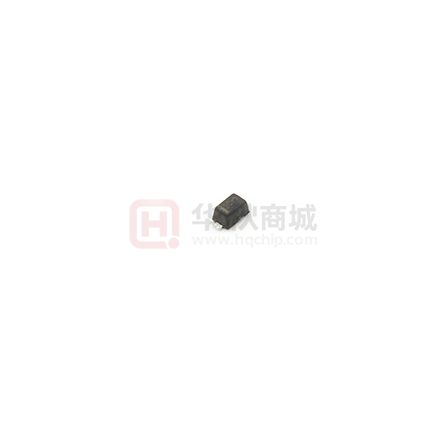
封装信息为SOD-523,引脚镀层为雾锡,外壳材料为“绿色”塑封料,UL阻燃等级为94V-0,湿度敏感等级为J-STD-020标准的3级,终端连接见下图,包装为3000pcs/7英寸胶带和卷轴。