WST2088A
N-Ch MOSFET
Product Summery
General Description
The WST2088A is the highest performance
trench N-ch MOSFETs with extreme high cell
density , which provide excellent RDSON and
gate charge for most of the small power
switching and load switch applications.
BVDSS
20V
RDSON
ID
10.7mΩ
7.5A
Applications
The WST2088A meet the RoHS and
Green Product requirement with full
function reliability approved.
● Power switching application
● Hard Switched and High Frequency Circuits
● Uninterruptible Power Supply
Features
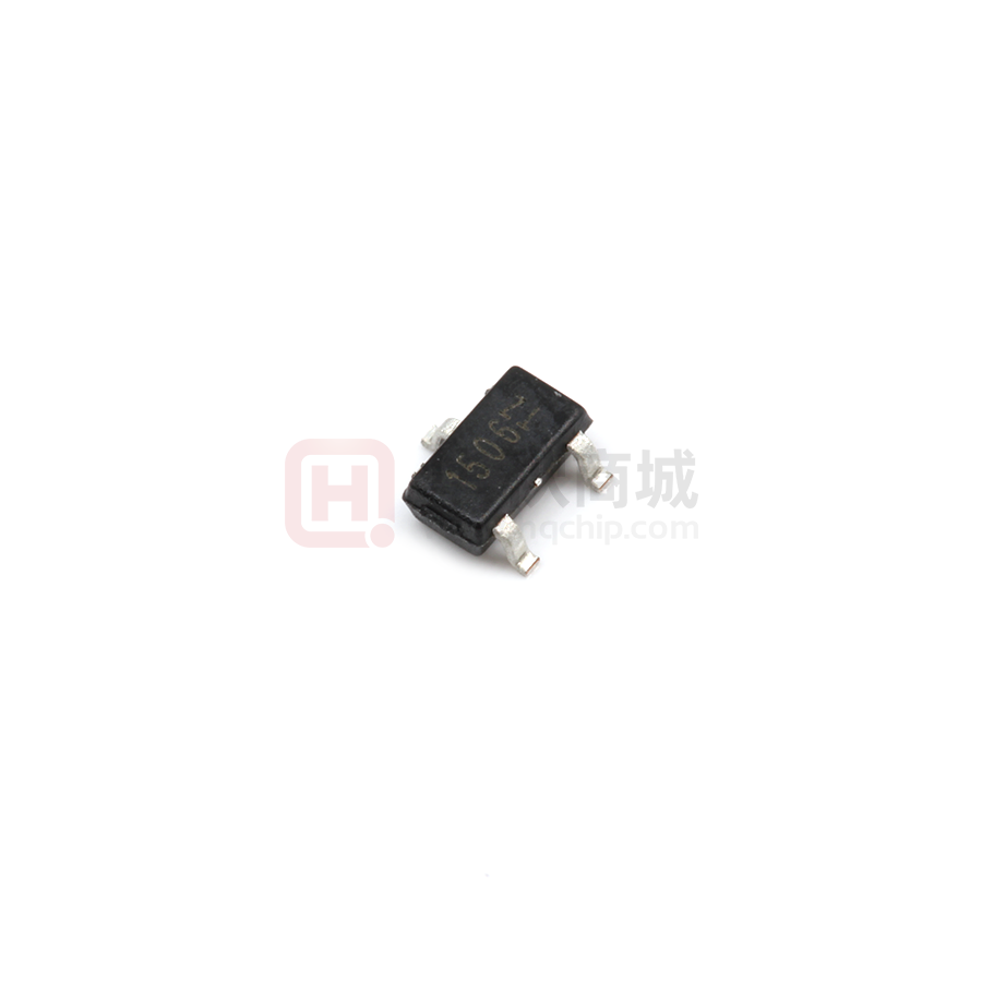
SOT-23-3L Pin Configuration
z Advanced high cell density Trench technology
z Super Low Gate Charge
z Excellent Cdv/dt effect decline
z Green Device Available
Absolute Maximum Ratings
Symbol
Parameter
Rating
Units
VDS
Drain-Source Voltage
20
V
VGS
Gate-Source Voltage
±12
V
ID@Tc=25℃
Continuous Drain Current, VGS @ 4.5V
7.5
A
ID@Tc=70℃
Continuous Drain Current, VGS @ 4.5V
4.5
A
IDP
Pulsed Drain Current
24
A
PD@TA=25℃
Total Power Dissipation
1.25
W
TSTG
Storage Temperature Range
-55 to 150
℃
TJ
Operating Junction Temperature Range
-55 to 150
℃
Thermal Data
Symbol
Rthj-a
Rthj-c
www.winsok.tw
Parameter
Typ.
Maximum Thermal Resistance, Junction-ambient
Maximum Thermal Resistance, Junction-case
Page 1
---
Max.
100
Unit
℃/W
---
8
℃/W
Rev:1.0 May.2019
�WST2088A
N-Ch MOSFET
Electrical Characteristics (TJ=25 ℃, unless otherwise noted)
Symbol
BVDSS
Parameter
Drain-Source Breakdown Voltage
△BVDSS/△TJ BVDSS Temperature Coefficient
RDS(ON)
Static Drain-Source On-Resistance2
Conditions
Min.
Typ.
Max.
Unit
VGS=0V , ID=250uA
20
---
---
V
Reference to 25℃ , ID=1mA
---
0.018
---
V/℃
---
10.7
14
VGS=2.5V , ID=5A
---
12.8
17
VGS=4.5V , ID=6A
mΩ
VGS=VDS , ID =250uA
0.4
0.63
1.2
IDSS
Drain-Source Leakage Current
VDS=16V , VGS=0V.
---
---
10
uA
IGSS
Gate-Source Leakage Current
VGS=±12V , VDS=0V
---
---
±100
nA
Qg
Total Gate Charge
---
10
---
Qgs
Gate-Source Charge
---
1.6
---
Qgd
Gate-Drain Charge
---
3.4
---
Turn-On Delay Time
---
8
---
VGS(th)
Td(on)
Tr
Td(off)
Tf
Ciss
Gate Threshold Voltage
VDS=15V , VGS=4.5V , ID=6A
V
nC
Rise Time
VDS=10V , VGS=4.5V ,
---
15
---
Turn-Off Delay Time
RG=3.3Ω ID=1A
---
33
---
---
13
---
---
590
---
---
125
---
---
90
---
Min.
Typ.
Max.
Unit
---
---
1.2
V
---
---
---
nS
---
---
---
nC
Fall Time
Input Capacitance
Coss
Output Capacitance
Crss
Reverse Transfer Capacitance
VDS=15V , VGS=0V , f=1MHz
ns
pF
Diode Characteristics
Symbol
Parameter
VSD
Diode Forward Voltage
trr
Reverse Recovery Time
Qrr
Reverse Recovery Charge
Conditions
VGS=0V , IS=1A
IF=1A , VGS=0V,
dI/dt=100A/µs
A: The value of RθJA is measured with the device mounted on 1in2 FR-4 board with 2oz. Copper, in a still air environment with TA=25°C. The value in any given
application depends on the user's specific board design.
B: Repetitive rating, pulse width limited by junction temperature.
C: The current rating is based on the t≤ 10s junction to ambient thermal resistance rating.
www.winsok.tw
Page 2
Rev:1.0 May.2019
�WST2088A
N-Ch MOSFET
Typical Characteristics
www.winsok.tw
Page 3
Rev:1.0 May.2019
�WST2088A
N-Ch MOSFET
www.winsok.tw
Page 4
Rev:1.0 May.2019
�Attention�
1,�Any�and�all�Winsok�power�products�described�or�contained�herein�do�not�have�specifications�that�can�handle�
applications�that�require�extremely�high�levels�of�reliability,�such�as�lifeͲsupport�systems,�aircraft's�control�systems,�or�
other�applications�whose�failure�can�be�reasonably�expected�to�result�in�serious�physical�and/or�material�damage.� �
Consult�with�your�Winsok�power�representative�nearest�you�before�using�any�Winsok�power�products�described�or�
contained�herein�in�such�applications.�
2,Winsok�power�assumes�no�responsibility�for�equipment�failures�that�result�from�using�products�at�values�that�exceed,� �
even�momentarily,�rated�values�(such�as�maximum�ratings,�operating�condition�ranges,�or�other�parameters)�listed�in�
products�specifications�of�any�and�all�Winsok�power�products�described�or�contained�herein.�
3,�Specifications�of�any�and�all�Winsok�power�products�described�or�contained�herein�stipulate�the�performance,�
characteristics,�and�functions�of�the�described�products�in�the�independent�state,�and�are�not�guarantees�of�the�
performance,�characteristics,�and�functions�of�the�described�products�as�mounted�in�the�customer’s�products�or�
equipment.�To�verify�symptoms�and�states�that�cannot�be�evaluated�in�an�independent�device,�the�customer�should�always�
evaluate�and�test�devices�mounted�in�the�customer’s�products�or�equipment.�
4,�Winsok�power�Semiconductor�CO.,�LTD.�strives�to�supply�highͲquality�highͲreliability�products.�However,�any�and�all�
semiconductor�products�fail�with�some�probability.�It�is�possible�that�these�probabilistic�failures�could�give�rise�to�accidents�
or�events�that�could�endanger�human�lives�that�could�give�rise�to�smoke�or�fire,�or�that�could�cause�damage�to�other�
property.�When�designing�equipment,�adopt�safety�measures�so�that�these�kinds�of�accidents�or�events�cannot�occur.�Such�
measures�include�but�are�not�limited�to�protective�circuits�and�error�prevention�circuits�for�safe�design,�redundant�design,�
and�structural�design.�
5,In�the�event�that�any�or�all�Winsok�power�products(including�technical�data,�services)�described�or�contained�herein�are�
controlled�under�any�of�applicable�local�export�control�laws�and�regulations,�such�products�must�not�be�exported�without�
obtaining�the�export�license�from�the�authorities�concerned�in�accordance�with�the�above�law.�
6,�No�part�of�this�publication�may�be�reproduced�or�transmitted�in�any�form�or�by�any�means,�electronic�or�mechanical,�
including�photocopying�and�recording,�or�any�information�storage�or�retrieval�system,�or�otherwise,�without�the�prior�
written�permission�of�Winsok�power�Semiconductor�CO.,�LTD.�
7,�Information�(including�circuit�diagrams�and�circuit�parameters)�herein�is�for�example�only;�it�is�not�guaranteed�for�
volume�production. Winsok�power�believes�information�herein�is�accurate�and�reliable,�but�no�guarantees�are�made�or�
implied�regarding�its�use�or�any�infringements�of�intellectual�property�rights�or�other�rights�of�third�parties.�
8,�Any�and�all�information�described�or�contained�herein�are�subject�to�change�without�notice�due�to�product/technology�
improvement,etc.�When�designing�equipment,�refer�to�the�"Delivery�Specification"�for�the�Winsok�power�product�that�you� �
Intend�to�use.�
9,�this�catalog�provides�information�as�of�Sep.2014. Specifications�and�information�herein�are�subject�to�change�without�
notice.�
�