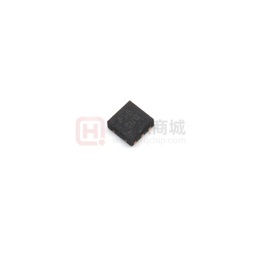
WSD2018ADN22
N-Ch MOSFET
Product Summery
General Description
The WSD2016ADN22 is the highest
performance trench N-Ch MOSFET with
extreme high cell density , which provide
excellent RDSON and gate charge for most of
the small power switching and load switch
applications.
BVDSS
RDSON
ID
20V
9.5mΩ
11A
Applications
The WSD2016ADN22 meet the RoHS and
Green Product requirement with full function
reliability approved.
z High Frequency Point-of-Load Synchronous s
Small power switching for MB/NB/UMPC/VGA
z Networking DC-DC Power System
z Load Switch
Features
DFNWB2×2-6L-J Pin Configuration
z Advanced high cell density Trench technology
z Super Low Gate Charge
z Excellent Cdv/dt effect decline
z Green Device Available
Absolute Maximum Ratings
Symbol
Parameter
VDS
VGS
ID@TC=25℃
ID@TC=70℃
IDM
Rating
Units
Drain-Source Voltage
20
V
Gate-Source Voltage
±10
V
1
11
A
1
9.5
A
40
A
Continuous Drain Current, VGS @ 4.5V
Continuous Drain Current, VGS @ 4.5V
Pulsed Drain Current
2
3
PD@TA=25℃
Total Power Dissipation
2.0
W
TSTG
Storage Temperature Range
-55 to 150
℃
TJ
Operating Junction Temperature Range
-55 to 150
℃
Thermal Data
Symbol
Parameter
RθJA
Thermal Resistance Junction-ambient
RθJC
1
www.winsok.tw
Thermal Resistance Junction-Case
Page 1
1
Typ.
Max.
Unit
---
167
℃/W
---
65
℃/W
Rev1.0 May.2019
�WSD2018ADN22
N-Ch MOSFET
Electrical Characteristics (TJ=25 ℃, unless otherwise noted)
Symbol
BVDSS
Parameter
Conditions
Drain-Source Breakdown Voltage
△BVDSS/△TJ BVDSS Temperature Coefficient
RDS(ON)
2
Static Drain-Source On-Resistance
Min.
Typ.
Max.
Unit
VGS=0V , ID=250uA
20
---
---
V
Reference to 25℃ , ID=1mA
---
0.027
---
V/℃
VGS=4.5V , ID=5A
---
9.5
12
VGS=2.5V , ID=5A
---
11
14
14.5
18
0.4
0.7
1.0
V
mV/℃
VGS=1.8V , ID=5A
VGS(th)
△VGS(th)
Gate Threshold Voltage
VGS(th) Temperature Coefficient
VGS=VDS , ID =250uA
---
2.56
---
VDS=16V , VGS=0V , TJ=25℃
---
---
1
VDS=16V , VGS=0V , TJ=55℃
---
---
5
mΩ
uA
IDSS
Drain-Source Leakage Current
IGSS
Gate-Source Leakage Current
VGS=±12V , VDS=0V
---
---
±100
nA
gfs
Forward Transconductance
VDS=4V , ID=9.7A
20
---
---
S
Rg
Gate Resistance
f=1MHz
---
2.5
---
Ω
Qg
Total Gate Charge (4.5V)
---
16
32
Qgs
Gate-Source Charge
---
1.3
---
Qgd
Gate-Drain Charge
---
1.6
---
VDS=4V , VGS=5V , ID=10A
---
16
20
Rise Time
VDD=4V , VGS=4.5V , RG=1Ω
---
25
45
Turn-Off Delay Time
ID=10A ,RL=0.4Ω
---
124
150
Fall Time
---
101
120
Ciss
Input Capacitance
---
1177
---
Coss
Output Capacitance
---
157
---
Crss
Reverse Transfer Capacitance
---
138
---
Td(on)
Tr
Td(off)
Tf
Turn-On Delay Time
VDS=4V , VGS=0V , f=1MHz
nC
ns
pF
Notes :
1.Surface mounted on FR4 board using 1 square inch pad size,1oz copper.
2.Surface mounted on FR4 board using the minimum pad size,1oz copper.
3. Pulse test : Pulse width=300μs, duty cycle≤2%.
4. These parameters have no way to verify.
www.winsok.tw
Page 2
Rev1.0 May.2019
�WSD2018ADN22
N-Ch MOSFET
Typical Characteristics
TYPICAL CHARACTERISTIC CURVES
Fig.1 On-Region Characteristics
Fig.2 Transfer Characteristics
Fig.3 On-Resistance vs. Drain Current
Fig.4 On-Resistance vs. Junction temperature
Fig.5 On-Resistance Variation with VGS
Fig.6 Body Diode Characteristics
www.winsok.tw
Page 3
Rev1.0 May.2019
�WSD2018ADN22
N-Ch MOSFET
TYPICAL CHARACTERISTIC CURVES
Fig.7 Gate-Charge Characteristics
Fig.9 Threshold Voltage Variation with Temperature
www.winsok.tw
Fig.8 Breakdown Voltage Variation vs. Temperature
Fig.10 Capacitance vs. Drain-Source Voltage
Page 4
Rev1.0 May.2019
�Outline Dimensions
DFNWB2X2-6L-J Package
Symbol
A
A1
A3
D
E
D1
E1
D2
E2
k
b
e
L
Dimensions In Millimeters
Min.
Max.
0.700
0.800
0.000
0.050
0.203REF.
1.924
2.076
1.924
2.076
0.800
1.000
0.850
1.050
0.200
0.400
0.460
0.660
0.200MIN.
0.250
0.350
0.650TYP.
0.174
0.326
Dimensions In Inches
Min.
Max.
0.032
0.000
0.002
0.008REF.
0.076
0.082
0.076
0.082
0.031
0.039
0.033
0.041
0.008
0.016
0.018
0.026
0.008MIN.
0.010
0.014
0.026TYP.
0.007
0.013
DFNWB2X2-6L-J Suggested Pad Layout
www.winsok.tw
Page 5
Rev1.0 May.2019
�Attention�
1,�Any�and�all�Winsok�power�products�described�or�contained�herein�do�not�have�specifications�that�can�handle�
applications�that�require�extremely�high�levels�of�reliability,�such�as�lifeͲsupport�systems,�aircraft's�control�systems,�or�
other�applications�whose�failure�can�be�reasonably�expected�to�result�in�serious�physical�and/or�material�damage.� �
Consult�with�your�Winsok�power�representative�nearest�you�before�using�any�Winsok�power�products�described�or�
contained�herein�in�such�applications.�
2,Winsok�power�assumes�no�responsibility�for�equipment�failures�that�result�from�using�products�at�values�that�exceed,� �
even�momentarily,�rated�values�(such�as�maximum�ratings,�operating�condition�ranges,�or�other�parameters)�listed�in�
products�specifications�of�any�and�all�Winsok�power�products�described�or�contained�herein.�
3,�Specifications�of�any�and�all�Winsok�power�products�described�or�contained�herein�stipulate�the�performance,�
characteristics,�and�functions�of�the�described�products�in�the�independent�state,�and�are�not�guarantees�of�the�
performance,�characteristics,�and�functions�of�the�described�products�as�mounted�in�the�customer’s�products�or�
equipment.�To�verify�symptoms�and�states�that�cannot�be�evaluated�in�an�independent�device,�the�customer�should�always�
evaluate�and�test�devices�mounted�in�the�customer’s�products�or�equipment.�
4,�Winsok�power�Semiconductor�CO.,�LTD.�strives�to�supply�highͲquality�highͲreliability�products.�However,�any�and�all�
semiconductor�products�fail�with�some�probability.�It�is�possible�that�these�probabilistic�failures�could�give�rise�to�accidents�
or�events�that�could�endanger�human�lives�that�could�give�rise�to�smoke�or�fire,�or�that�could�cause�damage�to�other�
property.�When�designing�equipment,�adopt�safety�measures�so�that�these�kinds�of�accidents�or�events�cannot�occur.�Such�
measures�include�but�are�not�limited�to�protective�circuits�and�error�prevention�circuits�for�safe�design,�redundant�design,�
and�structural�design.�
5,In�the�event�that�any�or�all�Winsok�power�products(including�technical�data,�services)�described�or�contained�herein�are�
controlled�under�any�of�applicable�local�export�control�laws�and�regulations,�such�products�must�not�be�exported�without�
obtaining�the�export�license�from�the�authorities�concerned�in�accordance�with�the�above�law.�
6,�No�part�of�this�publication�may�be�reproduced�or�transmitted�in�any�form�or�by�any�means,�electronic�or�mechanical,�
including�photocopying�and�recording,�or�any�information�storage�or�retrieval�system,�or�otherwise,�without�the�prior�
written�permission�of�Winsok�power�Semiconductor�CO.,�LTD.�
7,�Information�(including�circuit�diagrams�and�circuit�parameters)�herein�is�for�example�only;�it�is�not�guaranteed�for�
volume�production. Winsok�power�believes�information�herein�is�accurate�and�reliable,�but�no�guarantees�are�made�or�
implied�regarding�its�use�or�any�infringements�of�intellectual�property�rights�or�other�rights�of�third�parties.�
8,�Any�and�all�information�described�or�contained�herein�are�subject�to�change�without�notice�due�to�product/technology�
improvement,etc.�When�designing�equipment,�refer�to�the�"Delivery�Specification"�for�the�Winsok�power�product�that�you� �
Intend�to�use.�
9,�this�catalog�provides�information�as�of�Sep.2014. Specifications�and�information�herein�are�subject�to�change�without�
notice.�
�