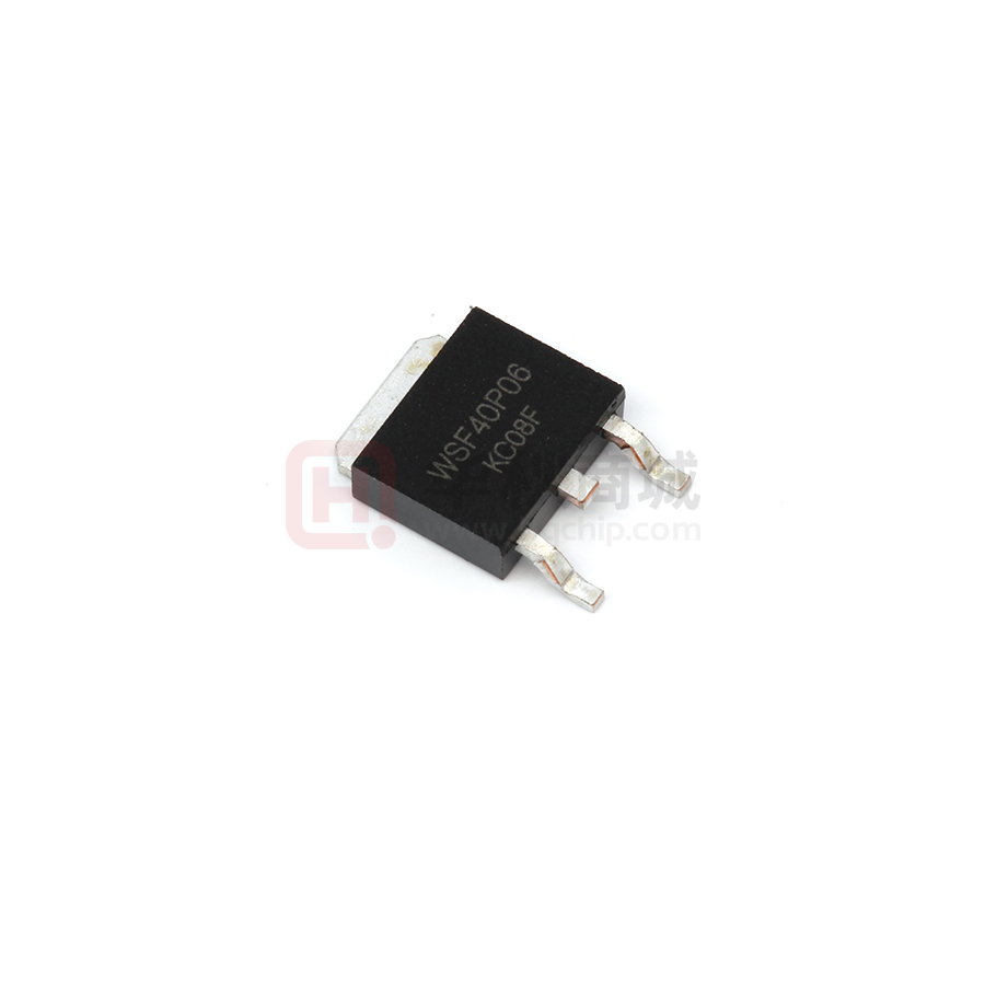
WSF40P06
P-Ch MOSFET
General Description
The WSF40P06 is the highest performance
trench P-ch MOSFETs with extreme high cell
density , which provide excellent RDSON and
gate charge for most of the synchronous
buck converter applications .
The WSF40P06 meet the RoHS and Green
Product requirement , 100% EAS
guaranteed with full function reliability
approved.
Product Summery
BVDSS
RDSON
ID
-60V
62mΩ
-17A
Applications
z Brushless motor
z Load switch
zUninterruptible power supply
Features
z Advanced high cell density Trench technology
TO-252 Pin Configuration
z Super Low Gate Charge
z Excellent CdV/dt effect decline
z 100% EAS Guaranteed
z Green Device Available
ABSOLUTE MAXIMUM RATINGS (TC = 25 °C Unless Otherwise Noted)
SYMBOL
PARAMETERS/TEST CONDITIONS
LIMITS
VDS
Drain‐Source Voltage
-60
VGS
Gate‐Source Voltage
±20
ID
Continuous Drain Current
TC = 25 °C
‐17
TC = 100 °C
‐11
IDM
Pulsed Drain Current1
‐60
IAS
Avalanche Current
‐12
EAS
Avalanche Energy
L = 0.1mH
7.2
EAR
Repetitive Avalanche Energy2
L = 0.05mH
3.6
PD
Power Dissipation
TC = 25 °C
27
TC = 100 °C
8
Tj, Tstg
Operating Junction & Storage Temperature Range
UNIT
V
A
mJ
W
‐55 to 150
°C
MAXIMUM
UNIT
THERMAL RESISTANCE RATINGS
SYMBOL
THERMAL RESISTANCE
RɵJC
Junction‐to‐Case
4.5
RɵJA
Junction‐to‐Ambient
85
www.winsok.tw
Page 1
°C / W
Rev1.0 May.2021
�WSF40P06
P-Ch MOSFET
P-Channel Electrical Characteristics (TJ=25 ℃, unless otherwise noted)
SYMBOL PARAMETER
TEST CONDITIONS
LIMITS
MIN
TYP
MAX
UNIT
STATIC
Drain‐Source Breakdown Voltage
VGS = 0V, ID = ‐250μA
‐60
---
---
Gate Threshold Voltage
VDS = VGS, ID = ‐250μA
‐1.0
‐1.8
‐3.0
IGSS
Gate‐Body Leakage
VDS = 0V, VGS = ±20V
---
---
±100
VDS = ‐48V, VGS = 0V
---
---
‐1
IDSS
Zero Gate Voltage Drain Current
VDS = ‐40V, VGS = 0V, TJ
= 125 °C
---
---
‐25
VDS = ‐5V, VGS = ‐4.5V
‐17
---
---
VGS = ‐10V, ID = ‐15A
---
55
62
VGS = ‐4.5V, ID = ‐7A
---
75
90
VDS = ‐5V, ID = ‐15A
---
12
---
---
1485
---
---
93
---
---
81
---
---
7.0
---
---
25.3
---
---
3.2
---
V(BR)DSS
VGS(th)
ID(ON)
RDS(ON)
gfs
On‐State Drain Current1
Drain‐Source On‐State Resistance1
Forward Transconductance1
V
nA
μA
A
mΩ
S
DYNAMIC
Ciss
Input Capacitance
Coss
Output Capacitance
Crss
Reverse Transfer Capacitance
Rg
Gate Resistance
Qg
Total Gate Charge1,2
VGS = 0V, VDS = ‐25V, f =
1MHz
VGS = 15mV, VDS = 0V, f =
1MHz
VDS = ‐30V, VGS = ‐10V, ID
= ‐10A
Qgs
Gate‐Source Charge1,2
Qgd
Gate‐Drain Charge1,2
---
4
---
td(on)
Turn‐On Delay Time1,2
---
12
---
---
24
---
---
45
---
---
60
---
tr
Rise Time1,2
td(off)
tf
Turn‐Off Delay Time1,2
VDS = ‐10V,
ID = ‐1A, VGS = ‐10V, RGS =
6Ω
Fall Time1,2
pF
Ω
nC
nS
SOURCE‐DRAIN DIODE RATINGS AND CHARACTERISTICS (TC = 25 °C)
IS
Continuous Current
---
---
‐17
ISM
Pulsed Current3
---
---
‐60
VSD
Forward Voltage1
---
---
1.3
V
---
12
---
nS
---
9
---
nC
trr
Reverse Recovery Time
Qrr
Reverse Recovery Charge
1Pulse
IF = IS, VGS = 0V
IF = ‐5A, dlF/dt = 100A/μS
A
test : Pulse Width≤300μsec, Duty Cycle≤ 2%.
2Independent
of operating temperature.
www.winsok.tw
Page 2
Rev1.0 May.2021
�WSF40P06
P-Ch MOSFET
TYPICAL CHARACTERISTICS
On‐Resistance Variation with Drain Current and Gate Voltage
On‐Region Characteristics
50
2.5
R ‐Normalized
DS(ON)
Drain‐Source On‐Resistance
V = ‐ 10.0V
GS
40
‐I ‐ Drain Current( A )
D
‐ 8.0V
30
‐ 7.0V
‐ 6.0V
20
‐ 5.0V
10
V = ‐ 4.5 V
GS
2
‐ 5.0 V
1.5
‐ 6.0 V
‐ 7.0 V
‐ 8.0 V
‐ 10.0 V
1
‐ 4.5V
0
0
4
6
8
‐V ‐ Drain‐Source Voltage( V )
DS
2
0.5
10
20
30
‐ I ‐ Drain Current( A )
D
40
0.20
I = ‐12 A
D
I = ‐ 6 A
D
R ‐ On‐Resistance(
Ω)
DS(ON)
1.3
1.0
0.7
0.15
0.10
T = 125°C
A
0.05
T = 25°C
A
0.4
‐50
‐25
0
25
50
75 100
T ‐ Junction Temperature (°C)
J
125
V = ‐ 10V
DS
50
T = ‐55°C
A
25°C
30
125°C
10
0
4.5
2.5
3.5
‐V ‐ Gate‐Source Voltage( V )
GS
www.winsok.tw
10
Body Diode Forward Voltage Variation
with Source Current and Temperature
100
40
20
4
6
8
‐ V ‐ Gate‐Source Voltage( V )
GS
2
Transfer Characteristics
60
1.5
0
150
‐Is ‐ Reverse Drain Current( A )
R ‐ Normalized
DS(on)
Drain‐Source On‐Resistance
V = ‐ 10V
GS
1.6
‐I ‐ Drain Current( A )
D
50
On‐Resistance Variation with Gate‐Source Voltage
On‐Resistance Variation with Temperature
1.9
10
0
5.5
10
V = 0V
GS
1
T = 125°C
A
0.1
25°C
‐55°C
0.01
0.001
0
Page 3
0.2
0.8
1.0
1.2
0.4
0.6
‐V ‐ Body Diode Forward Voltage( V )
SD
1.4
Rev1.0 May.2021
�WSF40P06
P-Ch MOSFET
Gate Charge Characteristics
10
Capacitance Characteristics
2500
8
V = ‐ 15V
DS
Capacitance( pF )
‐ 30V
6
4
Ciss
1500
1000
500
2
Coss
0
Crss
0
0
10
20
Q ‐ Gate Charge( nC )
g
30
40
it
Lim
N )
D S ( O
R
1ms
10ms
100ms
1s
10s
DC
V = ‐10V
GS
Single Pulse
R = 4.5°C/W
JC
T = 25°C
C
1
60
Single Pulse Maximum Power Dissipation
50
100μs
10
30
45
15
‐ V , Drain‐Source Voltage( V )
DS
0
Maximum Safe Operating Area
80
‐I ‐ Drain Current(A)
D
f = 1 MHz
V = 0 V
GS
2000
P(pk),Peak Transient Power(W)
‐ V ‐ Gate‐Source Voltage( V )
GS
I = ‐ 12A
D
Single Pulse
R = 4.5°C/W
θJC
T = 25°C
C
40
30
20
10
0
0
1
10
‐V ‐ Drain‐Source Voltage( V )
DS
100
0.001
0.01
0.1
t ,Time (sec)
1
1
10
100
Effective Transient Thermal Impedance
1
Normalized Thermal Response(R )
thjc
Duty Cycle = 0.5
0.2
0.1
0.1
Notes:
0.05
PDM
t1
0.02
t2
1.Duty Cycle,D =
t1
t2
2.R =4.5°C/W
θJC
0.01
3.T ‐ T = P * R (t)
J
C
θJC
Single Pulse
4.R (t)=r(t) * R
θJC
θJC
0.01
0.00001
www.winsok.tw
0.0001
0.001
t , Pulse Width(s)
1
0.01
Page 4
0.1
1
Rev1.0 May.2021
�Attention�
1,�Any�and�all�Winsok�power�products�described�or�contained�herein�do�not�have�specifications�that�can�handle�
applications�that�require�extremely�high�levels�of�reliability,�such�as�lifeͲsupport�systems,�aircraft's�control�systems,�or�
other�applications�whose�failure�can�be�reasonably�expected�to�result�in�serious�physical�and/or�material�damage.� �
Consult�with�your�Winsok�power�representative�nearest�you�before�using�any�Winsok�power�products�described�or�
contained�herein�in�such�applications.�
2,Winsok�power�assumes�no�responsibility�for�equipment�failures�that�result�from�using�products�at�values�that�exceed,� �
even�momentarily,�rated�values�(such�as�maximum�ratings,�operating�condition�ranges,�or�other�parameters)�listed�in�
products�specifications�of�any�and�all�Winsok�power�products�described�or�contained�herein.�
3,�Specifications�of�any�and�all�Winsok�power�products�described�or�contained�herein�stipulate�the�performance,�
characteristics,�and�functions�of�the�described�products�in�the�independent�state,�and�are�not�guarantees�of�the�
performance,�characteristics,�and�functions�of�the�described�products�as�mounted�in�the�customer’s�products�or�
equipment.�To�verify�symptoms�and�states�that�cannot�be�evaluated�in�an�independent�device,�the�customer�should�always�
evaluate�and�test�devices�mounted�in�the�customer’s�products�or�equipment.�
4,�Winsok�power�Semiconductor�CO.,�LTD.�strives�to�supply�highͲquality�highͲreliability�products.�However,�any�and�all�
semiconductor�products�fail�with�some�probability.�It�is�possible�that�these�probabilistic�failures�could�give�rise�to�accidents�
or�events�that�could�endanger�human�lives�that�could�give�rise�to�smoke�or�fire,�or�that�could�cause�damage�to�other�
property.�When�designing�equipment,�adopt�safety�measures�so�that�these�kinds�of�accidents�or�events�cannot�occur.�Such�
measures�include�but�are�not�limited�to�protective�circuits�and�error�prevention�circuits�for�safe�design,�redundant�design,�
and�structural�design.�
5,In�the�event�that�any�or�all�Winsok�power�products(including�technical�data,�services)�described�or�contained�herein�are�
controlled�under�any�of�applicable�local�export�control�laws�and�regulations,�such�products�must�not�be�exported�without�
obtaining�the�export�license�from�the�authorities�concerned�in�accordance�with�the�above�law.�
6,�No�part�of�this�publication�may�be�reproduced�or�transmitted�in�any�form�or�by�any�means,�electronic�or�mechanical,�
including�photocopying�and�recording,�or�any�information�storage�or�retrieval�system,�or�otherwise,�without�the�prior�
written�permission�of�Winsok�power�Semiconductor�CO.,�LTD.�
7,�Information�(including�circuit�diagrams�and�circuit�parameters)�herein�is�for�example�only;�it�is�not�guaranteed�for�
volume�production. Winsok�power�believes�information�herein�is�accurate�and�reliable,�but�no�guarantees�are�made�or�
implied�regarding�its�use�or�any�infringements�of�intellectual�property�rights�or�other�rights�of�third�parties.�
8,�Any�and�all�information�described�or�contained�herein�are�subject�to�change�without�notice�due�to�product/technology�
improvement,etc.�When�designing�equipment,�refer�to�the�"Delivery�Specification"�for�the�Winsok�power�product�that�you� �
Intend�to�use.�
9,�this�catalog�provides�information�as�of�Sep.2014. Specifications�and�information�herein�are�subject�to�change�without�
notice.�
�