85
DATA SHEET
SURFACE MOUNT MULTILAYER
CERAMIC CAPACITORS
High Frequency Automotive Grade
NP0
16 V TO 50 V
Product Specification – December 19, 2018 V.0
0.2 pF to 100 pF
RoHS compliant & Halogen Free
�Product specification
High Frequency
Automotive grade
Surface-Mount Ceramic Multilayer Capacitors
NP0
16 V to 50 V
2
15
SCOPE
ORDERING INFORMATION - GLOBAL PART NUMBER
This specification describes
Automotive grade NPO series
chip capacitors with lead-free
terminations and used for
automotive equipments.
All part numbers are identified by the series, size, tolerance, TC material,
packing style, voltage, process code, termination and capacitance value.
GLOBAL PART NUMBER
AQ
XXXX X X XXX X
(1)
APPLICATIONS
All general purpose applications
Entertainment applications
Comfort / security applications
Information applications
(2) (3) (4)
B
(5)
X XXX
(6) (7)
(1) SIZE – INCH BASED (METRIC)
0603 (1608)
(2) TOLERANCE
0.2pF to 2.0pF
A = ± 0.05 pF
FEATURES
AEC-Q200 qualified
MSL class: MSL 1
AC series soldering is
compliant with J-STD-020D
Halogen free epoxy
RoHS compliant
Reduce environmentally
hazardous waste
High component and
equipment reliability
The capacitors are 100%
performed by automatic optical
inspection prior to taping.
B = ± 0.1 pF
C = ± 0.25 pF
2.1pF to 5.0pF
A = ± 0.05 pF
B = ± 0.1 pF
C = ± 0.25 pF
D = ± 0.5 pF
5.1pF to 9.9pF
B = ± 0.1 pF
C = ± 0.25 pF
D = ± 0.5 pF
10pF and over
F = ± 1%
G = ± 2%
J = ± 5%
(3) PACKING STYLE
R = Paper/PE taping reel; Reel 7 inch
P = Paper/PE taping reel; Reel 13 inch
(4) TC MATERIAL
NPO
(5) RATED VOLTAGE
7 = 16 V
8 = 25 V
9 = 50 V
(6) PROCESS
N = NP0
(7) CAPACITANCE VALUE
2 significant digits+number of zeros
The 3rd digit signifies the multiplying factor, and letter R is decimal point
Example: 121 = 12 x 101 = 120 pF
www.yageo.com
Dec. 19, 2018 V.0
�Product specification
Surface-Mount Ceramic Multilayer Capacitors
High Frequency
Automotive grade
NP0
16 V to 50 V
3
15
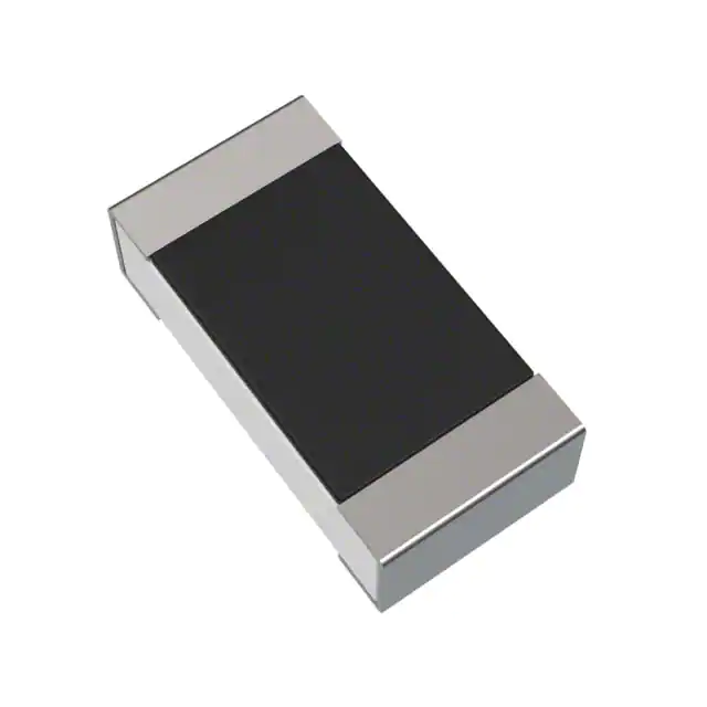
CONSTRUCTION
The capacitor consists of a
rectangular block of ceramic
dielectric in which a number of
interleaved metal electrodes are
contained. This structure gives
rise to a high capacitance per
unit volume.
The inner electrodes are
connected to the two end
terminations and finally covered
with a layer of plated tin (Matte
Sn). The terminations are leadfree. A cross section of the
structure is shown in Fig.1.
Fig. 1 Surface mounted multilayer ceramic capacitor construction
DIMENSION
OUTLINES
Table 1 For outlines see fig. 2
TYPE
0603
L1 (mm)
1.6 ± 0.10
W (mm)
0.8 ± 0.10
T (MM)
L2 / L3 (mm) L4 (mm)
min.
max.
min.
0.8 ± 0.10
0.20
0.60
For dimension see Table 1
0.40
Fig. 2 Surface mounted multilayer
ceramic capacitor dimension
www.yageo.com
Dec. 19, 2018 V.0
�Product specification
Surface-Mount Ceramic Multilayer Capacitors
CAPACITANCE RANGE & THICKNESS FOR NP0
Table 3 Sizes 0603
0603
CAP.
16 V
25 V
50 V
0.2 pF
0.8± 0.1
0.8± 0.1
0.8± 0.1
0.3 pF
0.8± 0.1
0.8± 0.1
0.4 pF
0.8± 0.1
0.5 pF
CAP.
High Frequency
Automotive grade
NP0
16 V to 50 V
4
15
0603
16 V
25 V
50 V
9 pF
0.8± 0.1
0.8± 0.1
0.8± 0.1
0.8± 0.1
10 pF
0.8± 0.1
0.8± 0.1
0.8± 0.1
0.8± 0.1
0.8± 0.1
12 pF
0.8± 0.1
0.8± 0.1
0.8± 0.1
0.8± 0.1
0.8± 0.1
0.8± 0.1
15 pF
0.8± 0.1
0.8± 0.1
0.8± 0.1
0.6 pF
0.8± 0.1
0.8± 0.1
0.8± 0.1
18 pF
0.8± 0.1
0.8± 0.1
0.8± 0.1
0.7 pF
0.8± 0.1
0.8± 0.1
0.8± 0.1
22 pF
0.8± 0.1
0.8± 0.1
0.8± 0.1
0.8 pF
0.8± 0.1
0.8± 0.1
0.8± 0.1
27 pF
0.8± 0.1
0.8± 0.1
0.8± 0.1
0.9 pF
0.8± 0.1
0.8± 0.1
0.8± 0.1
33 pF
0.8± 0.1
0.8± 0.1
0.8± 0.1
1.0 pF
0.8± 0.1
0.8± 0.1
0.8± 0.1
39 pF
0.8± 0.1
0.8± 0.1
0.8± 0.1
1.2 pF
0.8± 0.1
0.8± 0.1
0.8± 0.1
47 pF
0.8± 0.1
0.8± 0.1
0.8± 0.1
1.5 pF
0.8± 0.1
0.8± 0.1
0.8± 0.1
56 pF
0.8± 0.1
0.8± 0.1
0.8± 0.1
1.8 pF
0.8± 0.1
0.8± 0.1
0.8± 0.1
68 pF
0.8± 0.1
0.8± 0.1
0.8± 0.1
2.0 pF
0.8± 0.1
0.8± 0.1
0.8± 0.1
82 pF
0.8± 0.1
0.8± 0.1
0.8± 0.1
2.2 pF
0.8± 0.1
0.8± 0.1
0.8± 0.1
100 pF
0.8± 0.1
0.8± 0.1
0.8± 0.1
2.4 pF
0.8± 0.1
0.8± 0.1
0.8± 0.1
2.7 pF
0.8± 0.1
0.8± 0.1
0.8± 0.1
3.0 pF
0.8± 0.1
0.8± 0.1
0.8± 0.1
3.3 pF
0.8± 0.1
0.8± 0.1
0.8± 0.1
3.6 pF
0.8± 0.1
0.8± 0.1
0.8± 0.1
3.9 pF
0.8± 0.1
0.8± 0.1
0.8± 0.1
4.0 pF
0.8± 0.1
0.8± 0.1
0.8± 0.1
4.7 pF
0.8± 0.1
0.8± 0.1
0.8± 0.1
5.0 pF
0.8± 0.1
0.8± 0.1
0.8± 0.1
5.6 pF
0.8± 0.1
0.8± 0.1
0.8± 0.1
6.0 pF
0.8± 0.1
0.8± 0.1
0.8± 0.1
6.8 pF
0.8± 0.1
0.8± 0.1
0.8± 0.1
7.0 pF
0.8± 0.1
0.8± 0.1
0.8± 0.1
8.0 pF
0.8± 0.1
0.8± 0.1
0.8± 0.1
8.2 pF
0.8± 0.1
0.8± 0.1
0.8± 0.1
NOTE
1. Values in shaded cells indicate thickness class in mm
2. Capacitance value of non E-12 series is on request
www.yageo.com
Dec. 19, 2018 V.0
�Product specification
Surface-Mount Ceramic Multilayer Capacitors
High Frequency
Automotive grade
NP0
16 V to 50 V
5
15
THICKNESS CLASSES AND PACKING QUANTITY
Table 13
SIZE
CODE
0603
THICKNESS
CLASSIFICATION
TAPE WIDTH
QUANTITY PER REEL
0.8 ± 0.1 mm
8 mm
Ø 180 MM / 7 INCH
Paper
Blister
Ø 330 MM / 13 INCH
Paper
Blister
4,000
15,000
---
---
www.yageo.com
Dec. 19, 2018 V.0
�Product specification
Surface-Mount Ceramic Multilayer Capacitors
High Frequency
Automotive grade
NP0
6
15
16 V to 50 V
ELECTRICAL CHARACTERISTICS
NP0 DIELECTRIC CAPACITORS; NI/SIN TERMINATIONS
Unless otherwise specified, all test and measurements shall be made under standard atmospheric conditions
for testing as given in 5.3 of IEC 60068-1:
-
Temperature: 15 °C to 35 °C
Relative humidity: 25% to 75%
Air pressure: 86 kPa to 106 kPa
Before the measurements are made, the capacitor shall be stored at the measuring temperature for a time
sufficient to allow the entire capacitor to reach this temperature.
The period as prescribed for recovery at the end of a test is normally sufficient for this purpose.
Table 14
VALUE
DESCRIPTION
Capacitance range
0.2 pF to 100 µpF
Capacitance tolerance
NP0
C < 10 pF
±0.05 pF, ± 0.1 pF, ± 0.25 pF, ± 0.5 pF
C ≥ 10 pF
± 1%, ± 2%, ± 5%
Dissipation factor (D.F.)
NP0
C < 30 pF
≤ 1 / ( 400 + 20C )
C ≥ 30 pF
≤ 0.1 %
Insulation resistance after 1 minute at Ur (DC)
Maximum capacitance change as a function of temperature
(temperature characteristic/coefficient):
NP0
Operating temperature range:
NP0
IR ≥ 10 GΩ
± 30 ppm/°C
–55 °C to +125 °C
www.yageo.com
Dec. 19, 2018 V.0
�Product specification
Surface-Mount Ceramic Multilayer Capacitors
High Frequency
Automotive grade
NP0
7
15
16 V to 50 V
SOLDERING RECOMMENDATION
Table 15
SOLDERING
METHOD
SIZE
0402
0603
0805
1206
≥ 1210
Reflow
≥ 0.1 µF
≥ 1.0 µF
≥ 2.2 µF
≥ 4.7 µF
Reflow only
Reflow/Wave
< 0.1 µF
< 1.0 µF
< 2.2 µF
< 4.7 µF
---
SOLDERING CONDITIONS
The lead free MLCCs are able to stand the reflow soldering conditions as below:
Temperature: above 220 °C
Endurance: 95 to 120 seconds
Cycles: 3 times
The test of "soldering heat resistance" is carried out in accordance with the schedule of "MIL-STD-202F-method 210F", "The robust
construction of chip capacitors allows them to be completely immersed in a solder bath of 270 °C for 10 seconds". Therefore, it is possible
to mount MLCCs on one side of a PCB and other discrete components on the reverse (mixed PCBs). Surface Mount Capacitors are tested
for solderability at 245 °C during 2 seconds. The test condition for no leaching is 260°C for 30 seconds.
TESTS AND REQUIREMENTS
Table 16 Test procedures and requirements
TEST
Mounting
TEST METHOD
PROCEDURE
REQUIREMENTS
IEC 60384-
4.3
The capacitors may be mounted on printed-circuit
boards or ceramic substrates
No visible damage
4.5.1
Class 1:
At 20 °C, 24 hours after annealing
Within specified tolerance
21/22
Capacitance
IEC 6038421/22
f = 1 MHz for C ≤ 1nF, measuring at voltage 1 Vrms at
20 °C
f = 1 KHz for C > 1nF, measuring at voltage 1 Vrms at
20 °C
Dissipation
Factor (D.F.)
IEC 60384-
4.5.2
21/22
Class 1:
At 20 °C, 24 hours after annealing
In accordance with specification
f = 1 MHz for C ≤ 1nF, measuring at voltage 1 Vrms at
20 °C
f = 1 KHz for C > 1nF, measuring at voltage 1 Vrms at
20 °C
Insulation
Resistance
IEC 60384-
4.5.3
At Ur (DC) for 1 minute
In accordance with specification
21/22
www.yageo.com
Dec. 19, 2018 V.0
�Product specification
Surface-Mount Ceramic Multilayer Capacitors
TEST
TEST METHOD
4.6
Temperature
coefficient
High Frequency
Automotive grade
NP0
16 V to 50 V
PROCEDURE
REQUIREMENTS
Capacitance shall be measured by the steps shown in
the following table.
Class1:
∆ C/C: ± 30ppm
The capacitance change should be measured after 5
min at each specified temperature stage.
Step
Temperature(℃)
a
25± 2
b
Lower temperature± 3℃
c
25± 2
d
Upper Temperature± 2℃
e
25± 2
8
15
(1) Class I
Temperature Coefficient shall be calculated from the
formula as below
C2 - C1
Temp, Coefficient =
106 [ppm/℃]
C1 xΔT
C1: Capacitance at step c
C2: Capacitance at 125℃
∆T: 100℃(=125℃-25℃)
(2) Class II
Capacitance Change shall be calculated from the
formula as below
C2 - C1
∆C =
x 100%
C1
C1: Capacitance at step c
C2: Capacitance at step b or d
High
Temperature
Exposure
AEC-Q200
3
Unpowered ; 1000hours @ T=150℃
No visual damage
Measurement at 24± 2 hours after test conclusion.
Δ C/C:
Class1:
NP0: within ± 0.5% or 0.5 pF
whichever is greater
Temperature
Cycling
AEC-Q200
4
Preconditioning;
150 +0/–10 °C for 1 hour, then keep for
24 ± 1 hours at room temperature
1000 cycles with following detail:
30 minutes at lower category temperature
30 minutes at upper category temperature
Recovery time 24 ± 2 hours
Destructive
Physical Analysis
AEC-Q200
5
No visual damage
∆C/C
Class1:
NP0: Within ± 1% or 0.5pF,
whichever is greater.
D.F. meet initial specified value
IR meet initial specified value
10ea X 3 lots.
Note: Only applies to SMD ceramics.
Electrical test not required.
www.yageo.com
Dec. 19, 2018 V.0
�Product specification
Surface-Mount Ceramic Multilayer Capacitors
TEST
Moisture
Resistance
High Frequency
Automotive grade
NP0
16 V to 50 V
TEST METHOD
PROCEDURE
REQUIREMENTS
AEC-Q200
T=24 hrs/per cycle; 10 continuous cycles unpowered.
Measurement at 24 ± 2 hours after test condition.
No visual damage
6
9
15
∆C/C
NP0: Within ± 3% or 3 pF, whichever
is greater
D.F.
Within initial specified value
IR
NP0: ≥ 10,000 MΩ
Fig. 4 Moisture resistant
Biased Humidity
AEC-Q200
7
1. Preconditioning, class 2 only:
150 +0/-10 °C /1 hour, then keep for
24 ± 1 hour at room temp
No visual damage after recovery
2. Initial measure:
Parameter: IR
Measuring voltage: 1.5V ± 0.1 VDC
Note: Series with 100 KΩ & 6.8 KΩ
Initial requirement:
3. Test condition:
85 °C, 85% R.H. connected with 100 KΩ resistor,
applied 1.5V/Ur for 1,000 hours.
4. Recovery:
Class1: 6 to 24 hours
Class2: 24 ± 2 hours
5. Final measure: IR
Class1:
- Connected to 100 KΩ:
C ≤ 10 nF: I.R ≥ 10,000 MΩ or
C > 10 nF: (I.R-100 KΩ) x C ≥ 100s.
- Connected to 6.8 KΩ:
C ≤ 10 nF: I.R ≥ 10,000 MΩ or
C > 10 nF: (I.R-6.8 KΩ) x C ≥ 100s.
Final measurement:
The insulation resistance shall be
greater than 0.1 time initial value.
www.yageo.com
Dec. 19, 2018 V.0
�Product specification
Surface-Mount Ceramic Multilayer Capacitors
TEST
Operational Life
High Frequency
Automotive grade
NP0
TEST METHOD
PROCEDURE
REQUIREMENTS
AEC-Q200
1. Preconditioning, class 2 only:
150 +0/-10 °C /1 hour, then keep for
24 ± 1 hour at room temp
No visual damage
8
2. Initial measure:
Spec: refer to initial spec C, D, IR
3. Endurance test:
Specified stress voltage applied for 1,000 hours:
Applied 2.0 x Ur for general products
4. Recovery time: 24 ± 2 hours
5. Final measure: C, D, IR
10
16 V to 50 V
15
∆C/C
NP0: Within ± 2% or 1 pF, whichever
is greater
D.F.
NP0: ≤ 2 x specified value.
IR
NP0: ≥ 4,000 MΩ or IR x Cr ≥ 40s
whichever is less
Note: If the capacitance value is less than the minimum
value permitted, then after the other measurements
have been made the capacitor shall be preconditioned
according to “IEC 60384 4.1” and then the
requirement shall be met.
External Visual
AEC-Q200
9
Any applicable method using × 10 magnification
In accordance with specification
Physical
Dimension
AEC-Q200
10
Verify physical dimensions to the applicable device
specification.
In accordance with specification
Mechanical
Shock
AEC-Q200
13
Three shocks in each direction shall be applied along
the three mutually perpendicular axes of the test
specimen (18 shocks)
∆C/C
NP0: Within ± 0.5% or 0.5 pF,
whichever is greater
Peak value: 1,500 g’s
Duration: 0.5 ms
Velocity change: 15.4 ft/s
D.F.
Waveform: Half-sin
Within initial specified value
IR
Within initial specified value
Vibration
AEC-Q200
14
5 g’s for 20 minutes, 12 cycles each of 3 orientations.
Note:
Use 8” x 5” PCB. 0.31” thick 7 secure points on one
long side and 2 secure points at corners of opposite
sides. Parts mounted within 2” from any secure point.
Test from
10-2000 Hz.
Resistance to
Soldering Heat
AEC-Q200
15
Precondition: 150 +0/–10 °C for 1 hour, then keep for
24 ± 1 hours at room temperature
Preheating: for size ≤ 1206: 120 °C to 150 °C for 1
∆C/C
NP0: Within ± 0.5% or 0.5 pF,
whichever is greater
D.F: meet initial specified value
IR meet initial specified value
Dissolution of the end face plating
shall not exceed 25% of the length of
the edge concerned
www.yageo.com
Dec. 19, 2018 V.0
�Product specification
Surface-Mount Ceramic Multilayer Capacitors
TEST
TEST METHOD
High Frequency
Automotive grade
NP0
16 V to 50 V
PROCEDURE
REQUIREMENTS
minute
∆C/C
Preheating: for size >1206: 100 °C to 120 °C for 1
minute and 170 °C to 200 °C for 1 minute
Class1:
NP0: Within ± 1% or 0.5 pF,
whichever is greater.
Solder bath temperature: 260 ± 5 °C
11
15
Dipping time: 10 ± 0.5 seconds
Recovery time: 24 ± 2 hours
D.F. within initial specified value
IR within initial specified value
Thermal Shock
AEC-Q200
16
1. Preconditioning, class 2 only:
150 +0/-10 °C /1 hour, then keep for 24 ± 1 hour at
room temp
2. Initial measure:
Spec: refer to initial spec C, D, IR
No visual damage
∆C/C
NP0: Within ± 1% or 1 pF, whichever
is greater
3. Rapid change of temperature test:
NP0: -55 °C to +125 °C; 300 cycles
15 minutes at lower category temperature; 15
minutes at upper category temperature.
D.F: meet initial specified value
IR meet initial specified value
4. Recovery time:
Class1: 6 to 24 hours
Class2: 24 ± 2 hours
5. Final measure: C, D, IR
ESD
AEC-Q200
17
Per AEC-Q200-002
A component passes a voltage level if
all components stressed at that
voltage level pass.
Solderability
AEC-Q200
18
Preheated to a temperature of 80 °C to 140 °C and
maintained for 30 seconds to 60 seconds.
The solder should cover over 95% of
the critical area of each termination.
Test conditions for lead containing solder alloy
Temperature: 235 ± 5 °C
Dipping time: 2 ± 0.2 seconds
Depth of immersion: 10 mm
Alloy Composition: 60/40 Sn/Pb
Number of immersions: 1
Test conditions for lead-free containing solder alloy
Temperature: 245 ± 5 °C
Dipping time: 3 ± 0.3 seconds
Depth of immersion: 10 mm
Alloy Composition: SAC305
Number of immersions: 1
Electrical
Characterization
AEC-Q200
19
Parametrically test per lot and sample size
requirements, summary to show Min, Max, Mean and
Standard deviation at room as well as Min and Max
operating temperatures.
∆C/C
Class 1:
NP0: ± 30 ppm/°C
Class 1:
NP0: -55 °C to +125 °C
Normal temperature: 20 °C
www.yageo.com
Dec. 19, 2018 V.0
�Product specification
Surface-Mount Ceramic Multilayer Capacitors
TEST
Board Flex
High Frequency
Automotive grade
NP0
TEST METHOD
PROCEDURE
REQUIREMENTS
AEC-Q200
Part mounted on a 100 mm X 40 mm FR4 PCB board,
which is 1.6 ± 0.2 mm thick and has a layer-thickness 35
µm ± 10 µm.
Part should be mounted using the following soldering
reflow profile.
No visible damage
21
Conditions:
Class1:
Bending 3 mm at a rate of 1 mm/s, radius jig 340 mm
∆C/C
Class1:
NP0: Within ± 1% or 0.5 pF,
whichever is greater
Dimension(mm)
Test Substrate:
b
4.5
YNSC147Type
C
a
100
unit: mm
Terminal
Strength
AEC-Q200
22
With the component mounted on a PCB obtained
with the device to be tested, apply a 17.7N (1.8Kg)
force to the side of a device being tested.
This force shall be applied for 60+1 seconds.
Also the force shall be applied gradually as not to apply
a shock to the component being tested.
* Apply 2N force for 0402 size.
Beam Load Test
AEC-Q200
23
12
15
16 V to 50 V
Place the part in the beam load fixture. Apply a force
until the part breaks or the minimum acceptable force
level required in the user specification(s) is attained.
a
b
c
0201
0.3
0.9
0.3
0402
0.4
1.5
0.5
40 0603
1.0
3.0
1.2
0805
1.2
4.0
1.65
1206
2.2
5.0
1.65
1210
2.2
5.0
2.0
1808
3.5
7.0
3.7
Magnification of 20X or greater may
be employed for inspection of the
mechanical integrity of the device
body, terminals and body/terminal
junction.
Before, during and after the test, the
device shall comply with all electrical
requirements stated in this
specification.
≤ 0805
Thickness > 0.5mm: 20N
Thickness ≤ 0.5mm: 8N
≥ 1206
Thickness ≥1.25 mm: 54N
Thickness < 1.25 mm: 15N
Voltage Proof
1. Specified stress voltage applied for 1~5 seconds
No breakdown or flashover
2. Ur ≤ 100 V: series applied 2.5 Ur
3. 100 V < Ur ≤ 200 V series applied (1.5 Ur + 100)
4. 200 V < Ur ≤ 500 V series applied (1.3 Ur + 100)
5. Ur > 500 V: 1.3 Ur
6. Ur ≥ 1000 V: 1.2 Ur
Charge/Discharge current is less than 50 mA
www.yageo.com
Dec. 19, 2018 V.0
�Product specification
Surface-Mount Ceramic Multilayer Capacitors
TEST
ESR
TEST METHOD
High Frequency
Automotive grade
NP0
16 V to 50 V
13
15
PROCEDURE
REQUIREMENTS
Measuring frequency: 1 ± 0.2GHz at room
temperature.
0.2pF ≤ C ≤ 1pF : 350mΩ / C max
1pF < C ≤ 5pF : 300mΩ max
5pF < C ≤ 10pF : 250mΩ max
C : Nominal cap (pF)
Measuring frequency: 500 ± 50MHz at room
temperature.
10pF < C ≤ 100pF :400mΩ max
Note: Classify the components according to the highest ESD voltage level survived during
ESD testing.
Fig. 5 Passive component HBM ESD test flow diagram (DC = Direct Contact Discharge, AD = Air Discharge)
www.yageo.com
Dec. 19, 2018 V.0
�Product specification
Surface-Mount Ceramic Multilayer Capacitors
High Frequency
Automotive grade
NP0
16 V to 50 V
14
15
REVISION HISTORY
REVISION DATE
CHANGE NOTIFICATION
Version 0
-
Dec. 14, 2018
DESCRIPTION
- New
www.yageo.com
Dec. 19, 2018 V.0
�Product specification
Surface-Mount Ceramic Multilayer Capacitors
High Frequency
Automotive grade
NP0
16 V to 50 V
15
15
LEGAL DISCLAIMER
Yageo, its distributors and agents (collectively, “Yageo”), hereby disclaims any and all liabilities for any errors,
inaccuracies or incompleteness contained in any product related information, including but not limited to
product specifications, datasheets, pictures and/or graphics. Yageo may make changes, modifications and/or
improvements to product related information at any time and without notice.
Yageo makes no representation, warranty, and/or guarantee about the fitness of its products for any particular
purpose or the continuing production of any of its products. To the maximum extent permitted by law, Yageo
disclaims (i) any and all liability arising out of the application or use of any Yageo product, (ii) any and all
liability, including without limitation special, consequential or incidental damages, and (iii) any and all implied
warranties, including warranties of fitness for a particular purpose, non-infringement and merchantability.
Yageo statements regarding the suitability of products for certain types of applications are based on Yageo’s
knowledge of typical operating conditions for such types of applications in a gener ic nature. Such statements
are neither binding statements of Yageo nor intended to constitute any warranty concerning the suitability for a
specific customer application or use. They are intended for use only by customers with requisite knowledge and
experience for determining whether Yageo products are the correct products for their application or use. In
addition, unpredicatable and isolated cases of product failure may still occur, therefore, customer application or
use of Yageo products which requires higher degree of reliability or safety, shall employ additional protective
safeguard measures to ensure that product failure would not result in personal injury or property damage.
Yageo products are not designed for application or use in medical, life -saving, or life-sustaining devices or for
any other application or use in which the failure of Yageo products could result in personal injury or death.
Customers using or selling Yageo products not expressly indicated for above -mentioned purposes shall do so at
their own risk and agree to fully indemnify Yageo and hold Yageo harmless.
Information provided here is intended to indicate product specifications only. Yageo reserves all the rights for
revising this content without further notification, as long as products are unchanged. Any product change will
be announced by PCN.
www.yageo.com
Dec. 19, 2018 V.0
�


 工商网监
湘ICP备2023018690号
工商网监
湘ICP备2023018690号
