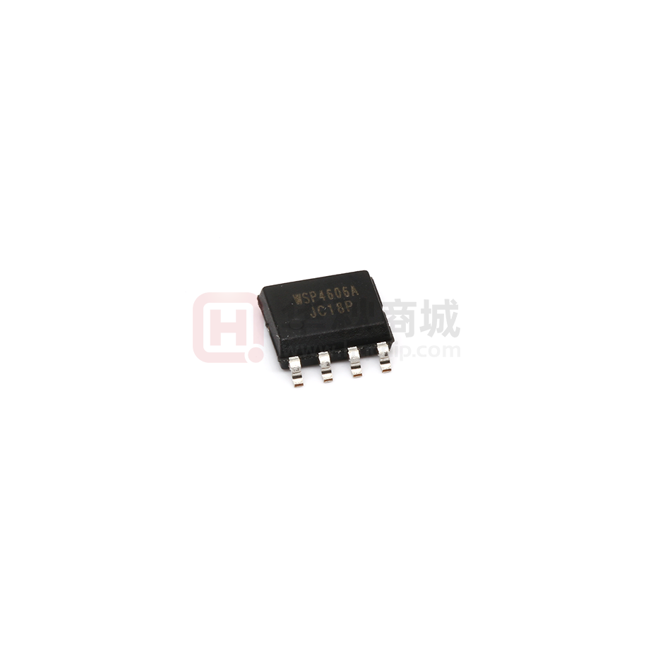
WSP4606A
N-Ch and P-Channel MOSFET
General Description
Product Summery
The WSP4606A is the highest performance
trench N-ch and P-ch MOSFETs with extreme
high cell density , which provide excellent
RDSON and gate charge for most of the
synchronous buck converter applications .
The WSP4606A meet the RoHS and Green
Product requirement , 100% EAS
guaranteed with full function reliability
approved.
BVDSS
RDSON
ID
30V
22mΩ
6.8A
-30V
45mΩ
-5.6A
Applications
z Power management in half bridge and inverters
z DC-DC Converter
Features
z Load Switch
z Advanced high cell density Trench technology
SOP-8 Pin Configuration
z Super Low Gate Charge
z Excellent CdV/dt effect decline
z 100% EAS Guaranteed
z Green Device Available
Absolute Maximum Ratings
Rating
Symbol
Parameter
VDS
Drain-Source Voltage
VGS
Gate-Source Voltage
ID@TC=25℃
ID@TC=100℃
IDM
N-Channel P-Channel
30
-30
V
±20
±20
V
1
6.8
-5.6
A
1
5.8
-3.9
A
19
-11
A
Continuous Drain Current, VGS @ 10V
Continuous Drain Current, VGS @ 10V
Pulsed Drain Current
Units
2
3
EAS
Single Pulse Avalanche Energy
71
58
mJ
IAS
Avalanche Current
20
-18
A
4
PD@TC=25℃
Total Power Dissipation
2.5
2.08
W
TSTG
Storage Temperature Range
-55 to 150
-55 to 150
℃
TJ
Operating Junction Temperature Range
-55 to 150
-55 to 150
℃
Max.
Unit
---
85
℃/W
---
50
℃/W
Thermal Data
Symbol
Parameter
Typ.
RθJA
Thermal Resistance Junction-Ambient
RθJC
Thermal Resistance Junction-Case1
www.winsok.tw
Page 1
1
Rev 2: Apr.2019
�WSP4606A
N-Ch and P-Channel MOSFET
Electrical Characteristics (TJ=25 ℃, unless otherwise noted)
Symbol
BVDSS
Parameter
Conditions
Drain-Source Breakdown Voltage
△BVDSS/△TJ BVDSS Temperature Coefficient
RDS(ON)
VGS(th)
Static Drain-Source On-Resistance2
Gate Threshold Voltage
Min.
Typ.
Max.
Unit
VGS=0V , ID=250uA
30
---
---
V
Reference to 25℃ , ID=1mA
---
0.034
---
V/℃
---
22
35
---
30
45
1.0
1.5
2.5
V
---
-5.8
---
mV/℃
VDS=30V , VGS=0V , TJ=25℃
---
---
1
VDS=30V , VGS=0V , TJ=55℃
---
---
5
VGS=10V , ID=6.3A
VGS=4.5V , ID=4.5A
VGS=VDS , ID =250uA
mΩ
△VGS(th)
VGS(th) Temperature Coefficient
IDSS
Drain-Source Leakage Current
IGSS
Gate-Source Leakage Current
VGS=±20V , VDS=0V
---
---
±100
nA
gfs
Forward Transconductance
VDS=15V , ID=5A
---
20
---
S
Rg
Gate Resistance
VDS=24V , VGS=0V , f=1MHz
---
1.8
---
Ω
Qg
Total Gate Charge (4.5V)
---
3.5
---
Qgs
Gate-Source Charge
---
1.3
---
Qgd
Gate-Drain Charge
---
1.7
---
VDS=20V , VGS=4.5V , ID=6A
uA
nC
---
4.5
---
Rise Time
VDD=12V , VGS=10V , RG=3.3Ω
---
2.7
---
Turn-Off Delay Time
ID=5A
---
14.9
---
Fall Time
---
2.9
---
Ciss
Input Capacitance
---
373
---
Coss
Output Capacitance
---
67
---
Crss
Reverse Transfer Capacitance
---
41
---
Min.
Typ.
Max.
Unit
A
Td(on)
Tr
Td(off)
Tf
Turn-On Delay Time
VDS=25V , VGS=0V , f=1MHz
ns
pF
Diode Characteristics
Symbol
Parameter
Conditions
1,6
IS
Continuous Source Current
ISM
Pulsed Source Current2,6
VSD
2
Diode Forward Voltage
VG=VD=0V , Force Current
VGS=0V , IS=5A , TJ=25℃
---
---
2.5
---
---
64
A
---
---
1.2
V
Note :
1.The data tested by surface mounted on a 1 inch2 FR-4 board with 2OZ copper,t
很抱歉,暂时无法提供与“WSP4606A”相匹配的价格&库存,您可以联系我们找货
免费人工找货- 国内价格
- 5+0.65638
- 50+0.53326
- 150+0.47170