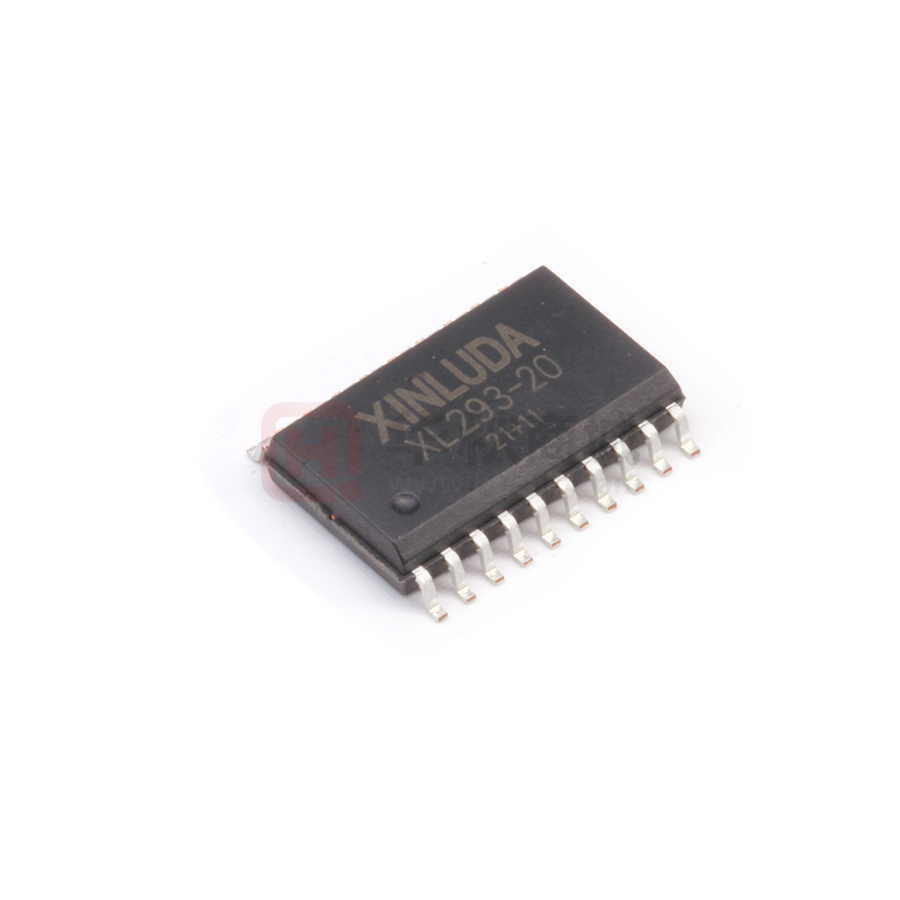
XD293-16 DIP16 XL293-20 SOP20
The XD293-16 is assembled in a 16 lead plastic
packaage which has 4 center pins connected together and used for heatsinking
The XL293-20 is assembled in a 20 lead surface
mount which has 8 center pins connected together and used for heatsinking.
600mA OUTPUT CURRENT CAPABILITY
PER CHANNEL
1.2A PEAK OUTPUT CURRENT (non repetitive) PER CHANNEL
ENABLE FACILITY
OVERTEMPERATURE PROTECTION
LOGICAL "0" INPUT VOLTAGE UP TO 1.5 V
(HIGH NOISE IMMUNITY)
INTERNAL CLAMP DIODES
DESCRIPTION
The Device is a monolithic integrated high voltage, high current four channel driver designed to
accept standard DTL or TTL logic levels and drive
inductive loads (such as relays solenoides, DC
and stepping motors) and switching power transistors.
To simplify use as two bridges each pair of channels is equipped with an enable input. A separate
supply input is provided for the logic, allowing operation at a lower voltage and internal clamp diodes are included.
This device is suitable for use in switching applications at frequencies up to 5 kHz.
BLOCK DIAGRAM
1
�XD293-16 DIP16 / XL293-20 SOP20
ABSOLUTE MAXIMUM RATINGS
Symbol
Parameter
Value
Unit
VS
Supply Voltage
36
V
VSS
Vi
Logic Supply Voltage
36
V
Ven
Io
Enable Voltage
Peak Output Current (100 µs non repetitive)
Ptot
Total Power Dissipation at Tpins = 90 °C
Tstg, Tj
Input Voltage
Storage and Junction Temperature
7
V
7
1.2
V
A
4
W
– 40 to 150
°C
PIN CONNECTIONS (Top view)
THERMAL DATA
Symbol
Decription
DIP
SO
Unit
Rth j-pins
Rth j-amb
Thermal Resistance Junction-pins
Thermal Resistance junction-ambient
max.
max.
–
80
14
50 (*)
°C/W
°C/W
Rth j-case
Thermal Resistance Junction-case
max.
14
–
(*) With 6sq. cm on board heatsink.
2
�XD293-16 DIP16 / XL293-20 SOP20
ELECTRICAL CHARACTERISTICS (for each channel, VS = 24 V, VSS = 5 V, Tamb = 25 °C, unless
otherwise specified)
Symbol
Parameter
Test Conditions
Min.
Typ.
Max.
Unit
VS
Supply Voltage (pin 10)
VSS
36
V
VSS
Logic Supply Voltage (pin 20)
4.5
36
V
IS
Total Quiescent Supply Current
(pin 10)
ISS
Total Quiescent Logic Supply
Current (pin 20)
Vi = L ; IO = 0 ; Ven = H
Vi = H ; IO = 0 ; Ven = H
2
16
6
24
mA
mA
Ven = L
Vi = L ; IO = 0 ; Ven = H
44
4
60
mA
mA
Vi = H ; IO = 0 ; Ven = H
16
22
mA
Ven = L
16
– 0.3
24
1.5
mA
V
2.3
2.3
VSS
7
V
V
– 10
µA
100
µA
– 0.3
1.5
V
2.3
2.3
VSS
7
V
V
– 100
µA
± 10
µA
VIL
Input Low Voltage (pin 2, 9, 12,
19)
VIH
Input High Voltage (pin 2, 9,
12, 19)
VSS ≤ 7 V
VSS > 7 V
IIL
Low Voltage Input Current (pin
2, 9, 12, 19)
VIL = 1.5 V
IIH
High Voltage Input Current (pin
2, 9, 12, 19)
2.3 V ≤ VIH ≤ VSS – 0.6 V
Ven L
Enable Low Voltage
(pin 1, 11)
Ven H
Enable High Voltage
(pin 1, 11)
VSS ≤ 7 V
VSS > 7 V
Ien L
Low Voltage Enable Current
(pin 1, 11)
Ven L = 1.5 V
Ien H
High Voltage Enable Current
(pin 1, 11)
Source Output Saturation
Voltage (pins 3, 8, 13, 18)
Sink Output Saturation Voltage
(pins 3, 8, 13, 18)
Clamp Diode Forward Voltage
2.3 V ≤ Ven H ≤ VSS – 0.6 V
tr
tf
ton
toff
VCE(sat)H
VCE(sat)L
VF
30
– 30
IO = – 0.6 A
1.4
1.8
V
IO = + 0.6 A
1.2
1.8
V
IO = 600nA
1.3
V
Rise Time (*)
0.1 to 0.9 VO
250
ns
Fall Time (*)
Turn-on Delay (*)
Turn-off Delay (*)
0.9 to 0.1 VO
0.5 Vi to 0.5 VO
0.5 Vi to 0.5 VO
250
750
200
ns
ns
ns
(*) See fig. 1.
3
�XD293-16 DIP16 / XL293-20 SOP20
Figure 1: Switching Times
TRUTH TABLE (one channel)
Input
Enable (*)
Output
H
L
H
L
H
H
L
L
H
L
Z
Z
Z = High output impedance
(*) Relative to the considered channel
Figure 2: Junction to ambient thermal resistance vs. area on board heatsink
4
�XD293-16 DIP16 / XL293-20 SOP20
SOP
54
�XD293-16 DIP16 / XL293-20 SOP20
DIP
46
�
很抱歉,暂时无法提供与“XL293-20”相匹配的价格&库存,您可以联系我们找货
免费人工找货