SL210N06
N-Channel Power MOSFET
General Description
Features
This type used advanced trench technology and
design to provide excellent RDS(ON) with low gate
charge.
l
High density cell design for ultra low RDS(ON)
l
Excellent package for good heat dissipation
For a single MOSFET
l
l
l
VDS = 60V
RDS(ON) = 2.2mΩ @ VGS=10V
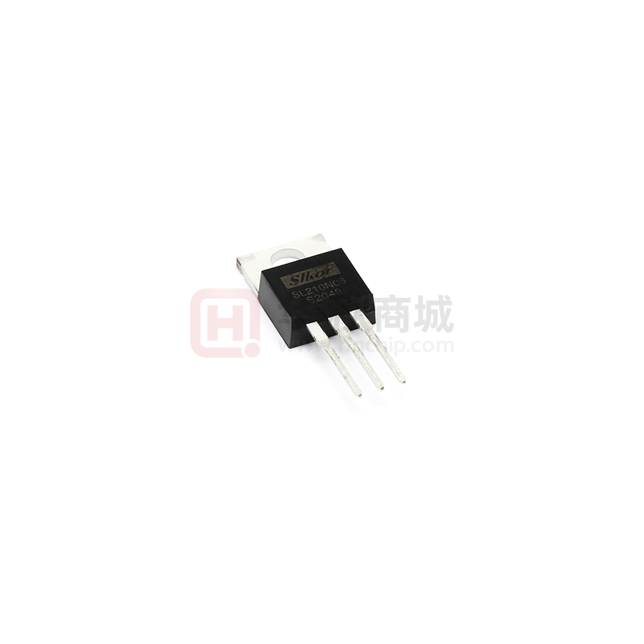
Pin configurations
See Diagram below
Absolute Maximum Ratings
Parameter
Symbol
Rating
Units
Drain-Source Voltage
VDS
60
V
Gate-Source Voltage
VGS
±20
V
Continuous
210
Drain Current
ID
Pulsed
Total Power Dissipation
@TA=25℃
Operating Junction Temperature Range
www.slkormicro.com
A
800
1
PD
300
W
TJ
-55 to 175
℃
�SL210N06
Electrical Characteristics (TJ=25℃ unless otherwise noted)
Symbol
Parameter
Test Conditions
Min
Typ
Max
Units
OFF CHARACTERISTICS (Note 2)
BVDSS
Drain-Source Breakdown Voltage
ID=250μA, VGS=0 V
IDSS
Drain to Source Leakage Current
VDS= 48V, VGS=0V
IGSS
Gate-Body Leakage Current
VGS=20V
Gate Threshold Voltage
VDS= VGS, ID=250μA
VGS(th)
RDS(ON)
Static Drain-Source On-Resistance
VGS=10V, ID=20A
60
2.0
V
1
μA
100
nA
3.0
4.0
V
2.2
2.6
mΩ
DYNAMIC PARAMETERS
Ciss
Input Capacitance
VGS=0V, VDS=30V,
Coss
Output Capacitance
Crss
Reverse Transfer Capacitance
f=1MHz
7070
pF
2140
pF
63
pF
85
nC
24
nC
14
nC
SWITCHING PARAMETERS
Qg
Total Gate Charge
2
VGS=10V, VDS=30V,
Qgs
Gate Source Charge
Qgd
Gate Drain Charge
td(on)
Turn-On Delay Time
VGS=10V, VDS=30V,
36
ns
td(off)
Turn-Off Delay Time
RGEN=10Ω
95
ns
td(r)
Turn-On Rise Time
62
ns
td(f)
Turn-Off Fall Time
34
ns
ID=20A
Thermal Resistance
Symbol
RθJC
Parameter
Typ
Units
Junction to Case
0.5
℃/W
www.slkormicro.com
2
�SL210N06
Typical Characteristics
www.slkormicro.com
3
�SL210N06
Typical Characteristics
www.slkormicro.com
4
�SL210N06
Package Outline Dimension
TO-220
www.slkormicro.com
5
�
很抱歉,暂时无法提供与“SL210N06”相匹配的价格&库存,您可以联系我们找货
免费人工找货- 国内价格
- 1+3.51000
- 10+3.38000
- 100+3.06800
- 500+2.91200