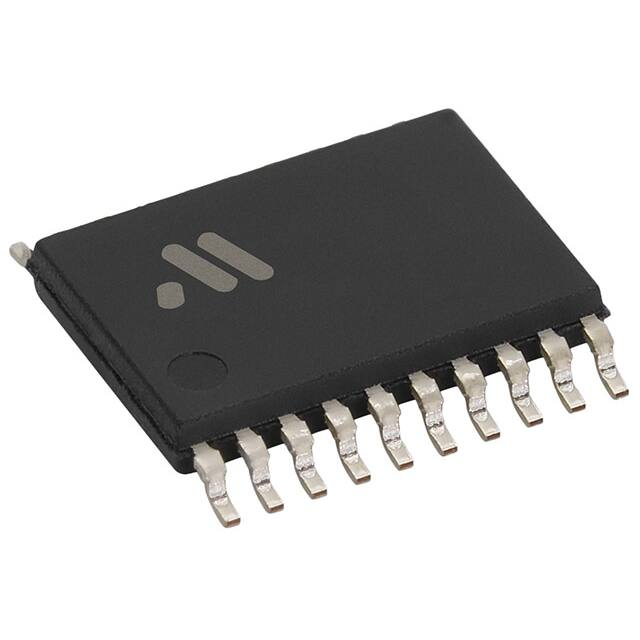
3 to 5cells lithium-ion / lithium-polimar secondary battery protection IC
3 to 5cells lithium-ion / lithium-polimar secondary battery protection IC
MM3474 Series
Description
MM3474 series is an overcharge, overdischarge and overcurrent protection IC for a lithium-ion / lithium-polymer secondary
battery. This supports 3 to 5 serial cells, and the number of cells can be switched over by inputting high / low signal to SEL
terminal. MM3474 series can protect Lithium ion battery pack of 6-plus serial cells by connecting in cascade. This also provides
the control terminals of output overdischarge detection (SDC) and output overcharge detection (SOC), which allows configuring
an application with fewer external parts for 6 or more cells connected in series.
We provide many kinds of optional ICs of MM3474 series, which are customizable for the usage by selecting optional functions.
Low cost and small size configuration can be achieved when MM3474 series is combined with MM3220V series which is 2 cells
protection IC and used for the applications of 6 cells or 7 cells, etc.
Cell balance control function can be added when MM3513 series which is cell balance control IC is used.
Features
(Unless otherwise specified, Ta=25 degC)
・Detection voltage
Range
Accuracy
Overcharge detection voltage
3.6V to 4.5V, 5mV steps
+/-25mV(Ta=0 to +50 degC)
Overdischarge detection voltage
2.0V to 3.0V, 50mV steps
+/-80mV
Overcurrent detection voltage
50mV to 300mV, 5mV steps
+/-15mV
Short detection voltage
0.2V to 1.0mV, 50mV steps
+/-100mV
・3-, 4-, 5-cell protection switching function
The 3-, 4-, or 5-cell protection can be switched by connecting the SEL1 pin and SEL2 pin to the VDD or VSS2 via a protection
resistor. At the time of 4-cell protection, the operation of the overcharge detection circuit and overdischarge detection circuit
for the V1 cell is stopped. Therefore, short-circuit the V1 pin and VSS1 pin before use. At the time of 3-cell protection, the
operation of overcharge detection circuit and overdischarge detection circuit for V1 and V2 Cell is stopped. Therefore, shortcircuit the V2 pin, V1 pin and VSS1 pin before use.
SEL1 pin
SEL2 pin
MM3474 Setting
High (VDD)
High (VDD)
5 cell prptection
High (VDD)
Low (VSS2)
4 cell prptection
Low (VSS2)
High (VDD)
3 cell prptection
Low (VSS2)
Low (VSS2)
prohibite
・Communication function when cascade connected
When using a cascade-connected IC with 6 or more cell protection, an overdischarge detection signal can be transmitted by
inputting the DCHG output pin signal to the SDC pin via a resistor. If the current input to the SDC pin exceeds the SDC release
current, it is recognized as normal state. If it drops below the SDC detection current or if it is open, it is recognized as
overdischarge detection state. In the same way, an overdischarge detection signal can be transmitted by inputting the OV
output pin signal to the SOC pin via a resistor.
In addition, charge / discharge is more controllable than inputting a signal into SDC terminal, SOC terminal from the outside
independently.
Applications
・Lithium-ion rechargeable battery pack
・Lithium polymer rechargeable battery pack
Package type
・TSOP-20C/20D
6.50 × 6.40 × 1.10 [mm]
1
�3 to 5cells lithium-ion / lithium-polimar secondary battery protection IC
Block diagram
Overdischarge release : 「Voltage release」 type
2
�3 to 5cells lithium-ion / lithium-polimar secondary battery protection IC
Block diagram
Overdischarge release : 「Load release + Voltage release」 type
3
�3 to 5cells lithium-ion / lithium-polimar secondary battery protection IC
Package and pin configuration
Pin No.
Pin No.
Function
1
OV
Charge control output terminal. Output type is Pch open drain. Active "Hi impedance".
2
V-
Input terminal connected to charger negative voltage. Detected charger connection and load detection.
3
CS
Input of overcurrent detection. The voltage of the sense resistance is observed, and the overcurrent is detected.
4
DCHG
5
COV
This pin is dead time setting of overcharge detection and release.
6
CDC
This pin is dead time setting of overdischarge detection and release.
7
COL1
This pin is dead time setting of overcurrent detection.
8
COL2
This pin is dead time setting of overcurrent release.
9
VSS1
The input terminal of the negative voltage of V1 cell .
10
VSS2
The input terminal of the ground of IC.
11
SEL1
12
SEL2
This pin is for changing function for 3cell in series or 4cell in series , 5cell in series.
SEL1 = H , SEL2 = H → 5Cell protection
SEL1 = H , SEL2 = L → 4Cell protection
SEL1 = L , SEL2 = H → 3Cell protection (SEL1=SEL2=L setting is prohibited. )
13
V1
The input terminal of the positive voltage of V1 cell, and the negative voltage of V2 cell .
14
V2
The input terminal of the positive voltage of V2 cell, and the negative voltage of V3 cell .
15
V3
The input terminal of the positive voltage of V3 cell, and the negative voltage of V4 cell .
16
V4
The input terminal of the positive voltage of V4 cell, and the negative voltage of V5 cell .
17
V5
The input terminal of the positive voltage of V5 cell .
18
VDD
19
SDC
20
SOC
Discharge control output terminal. Output type is CMOS. Active "Low".
The input terminal of the power supply of IC.
I
I
SDC
很抱歉,暂时无法提供与“MM3474F03VBE”相匹配的价格&库存,您可以联系我们找货
免费人工找货