IS31BL3229
8-LED BACKLIGHT DRIVER
July 2021
GENERAL DESCRIPTION
FEATURES
The IS31BL3229 with a smart charge-pump circuit is a
parallel white-LED driver with eight matched 20mA
current outputs. It can supply a total output current of
160mA over an input voltage range of 2.7V to 5.5V.
IS31BL3229 typically draws less than 1µA when placed
in shutdown, and 0.7mA when operating in the no-load
and 1X mode condition. If any of the outputs are not
used, leave the pin(s) unconnected. Brightness can be
controlled by simple-series-control techniques and
external PWM signal.
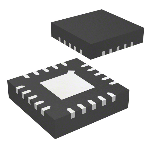
IS31BL3229 is available in QFN-20 (3mm × 3mm). It
operates from 2.7V to 5.5V over the temperature range
of -40°C to +85°C.
Supply voltage: 2.7V ~ 5.5V
1X, 1.5X operating mode
fade in and fade out mode
Output current can be 25mA
32 current level and PWM intensity control
Low input current ripple, low EMI
90% high efficiency
No inductors, low noise operation
Over voltage protection on output
Built-in thermal protection
Automatic soft start
Built-in thermal protection
QFN-20 (3mm × 3mm ) package
APPLICATIONS
Cell phone, smart phone, PDA
Mp3, Mp4, PMP
White LED backlighting
TYPICAL APPLICATION CIRCUIT
Figure 1
Typical Application Circuit
Note 1: PWM pin should be pulled high if modulated by EN pin only. EN pin should be pulled high if modulated with PWM pin only. Please refer
to Page 8 for detail information.
Note 2: The fade in and fade out mode is only available when shut down and enable the IC by EN pin.
Note 3: D1 must be connected and others can be floating in less than 8 LEDs application.
Note 4: The IC should be placed far away from the mobile antenna in order to prevent the EMI.
Lumissil Microsystems – www.lumissil.com
Rev.B, 07/15/2021
1
�IS31BL3229
PIN CONFIGURATION
20 CN1
19 CP1
18 OUT
17 D1
16 D2
RSET 7
OPT 8
GND 9
D8 10
Pin Configuration (Top View)
PWM 6
Package
QFN-20
PIN DESCRIPTION
No.
Pin
Description
1
NC
No connection.
2
VCC
Power supply input, requires 0.1μF and 1μF capacitor
connect between this pin and ground pin.
3
CP2
Flying capacitor positive terminal 2.
4
CN2
Flying capacitor negative terminal 2.
5
EN
Shutdown and output current control pin. Pull low to
shutdown the IC.
6
PWM
PWM control pin. Adjust the LED intensity by PWM duty
cycle. Pull low at least 128ms (Typ.), the IC should be
shutdown.
7
RSET
8
OPT
Option pin. Floating to operating in FIFO mode. Pull low to
disable FIFO.
9
GND
Ground.
10~17
D8~D1
White LED channel 8~1. D1 must be connected and
others can be floating in less than 8 LEDs application.
18
OUT
Charge pump output to drive load circuits, Requires 1μF
capacitor connected between this pin and ground pin.
19
CP1
Flying capacitor positive terminal 1.
20
CN1
Flying capacitor negative terminal 1.
Thermal Pad
Connect to GND.
External resistor for bias current.
I MAX 1.25 / RSET 1600
Lumissil Microsystems – www.lumissil.com
Rev.B, 07/15/2021
2
�IS31BL3229
ORDERING INFORMATION
Industrial Range: -40°C to +85°C
Order Part No.
Package
QTY/Reel
IS31BL3229-QFLS2-TR
QFN-20, Lead-free
2500
Copyright © 2021 Lumissil Microsystems. All rights reserved. Lumissil Microsystems reserves the right to make changes to this specification and its
products at any time without notice. Lumissil Microsystems assumes no liability arising out of the application or use of any information, products or
services described herein. Customers are advised to obtain the latest version of this device specification before relying on any published information and
before placing orders for products.
Lumissil Microsystems does not recommend the use of any of its products in life support applications where the failure or malfunction of the product can
reasonably be expected to cause failure of the life support system or to significantly affect its safety or effectiveness. Products are not authorized for use in
such applications unless Lumissil Microsystems receives written assurance to its satisfaction, that:
a.) the risk of injury or damage has been minimized;
b.) the user assume all such risks; and
c.) potential liability of Lumissil Microsystems is adequately protected under the circumstances
Lumissil Microsystems – www.lumissil.com
Rev.B, 07/15/2021
3
�IS31BL3229
ABSOLUTE MAXIMUM RATINGS
Supply voltage, VCC
Voltage at any input pin
Junction temperature, TJMAX
Storage temperature range, TSTG
Operating temperature ratings, TA
-0.3V ~ +6.0V
-0.3V ~ VCC+0.3V
+150°C
-65°C ~ +150°C
-40°C ~ +85°C
Note: Stresses beyond those listed under “Absolute Maximum Ratings” may cause permanent damage to the device. These are stress ratings
only and functional operation of the device at these or any other condition beyond those indicated in the operational sections of the specifications
is not implied. Exposure to absolute maximum rating conditions for extended periods may affect device reliability.
ELECTRICAL CHARACTERISTICS
VCC = 2.7V ~ 5.5V, TA = 25°C, unless otherwise noted. Typical value are TA = 25°C, VCC = 3.6V.
Symbol
Parameter
VCC
Operation range
ICC
Operating current
ISD
Shutdown current
IOUT
Output current
ILED
LED current for each channel
I(D-Match)
VTH
Condition
Min.
Typ.
2.7
1x mode, no load
Max.
Unit
5.5
V
0.7
1.5x mode, no load
2
VEN = 0V
1
mA
μA
200
RSET = 100kΩ
Current matching between any two outputs
mA
20
mA
1
%
Transition threshold (D1 pin)
VD1 falling
180
mV
VUVLO
Input under voltage lockout threshold
VCC rising or falling.
100mV hysteresis
2.4
V
VSET
Bias voltage for RSET pin
1.25
V
VOVP
Over voltage protect
5.5
V
tFI
Fade in time
FIFO Mode(Note 5)
400
ms
tFO
Fade out time
400
ms
RDS_ON
Output resistor
160
°C
TOTP
Over temperature protection
FIFO Mode(Note 5)
1x mode:
(VCC-VOUT)/IOUT
(Note 6)
THYS
Over temperature protection hysteresis
(Note 6)
40
°C
1
Ω
Charge Pump Characteristics
tST
Soft-start time
(Note 6)
150
μs
fCLK
Clock frequency
(Note 6)
1
MHz
Lumissil Microsystems – www.lumissil.com
Rev.B, 07/15/2021
4
�IS31BL3229
ELECTRICAL CHARACTERISTICS (Continue)
VCC = 2.7V ~ 5.5V, TA = 25°C, unless otherwise noted. Typical value are TA = 25°C, VCC = 3.6V.
Symbol
Parameter
Condition
Min.
Typ.
Max.
Unit
0.4
V
EN, PWM Pin Characteristics
VIL
Enable threshold low
VCC = 2.7V
VIH
Enable threshold high
VCC = 5.5V
1.4
tLO
EN low time
(Note 6)
0.5
75
μs
tHI
EN high time
(Note 6)
0.5
75
μs
tOFF
EN off time
(Note 6)
500
μs
tLAT
EN latch time
(Note 6)
500
μs
fPWM
Input frequency for PWM pin
tOFF_PWM
PWM off time
V
0.1
(Note 7)
50
128
kHz
ms
Note 5: Typical value.
Note 6: Guaranteed by design.
Note 7: As the PWM pin is pulled low at least 128ms, the IS31BL3229 will be shutdown.
Lumissil Microsystems – www.lumissil.com
Rev.B, 07/15/2021
5
�IS31BL3229
TYPICAL PERFORMANCE CHARACTERISTIC
100
25
20
80
70
Efficiency(%)
Output Current(mA)
90
15
10
5
60
50
40
30
VEN = VPWM = 3.6V
VF = 3.2V
ILED = 20mA
RSET = 100kΩ
20
VEN = VPWM = 3.6V
RSET = 100kΩ
0
2.7
3
10
4
3.5
4.5
0
2.7
5
3
3.5
100
18
90
16
80
14
70
Duty Cycle(%)
Output Current(mA)
Figure 3
Supply Voltage vs. Output Current
20
12
10
8
6
5
Supply Voltage vs. Efficiency
RSET = 100kΩ
VEN = VCC = 3.6V
fPWM = 1kHz
60
50
40
30
20
4
RSET = 100kΩ
VPWM = VCC = 3.6V
2
0
4.5
Supply Voltage(V)
Supply Voltage(V)
Figure 2
4
1
4
8
10
12
16
20
24
28
32
0
0
5
EN Level
Figure 4
EN pin dimming
Lumissil Microsystems – www.lumissil.com
Rev.B, 07/15/2021
10
15
20
Output Current(mA)
Figure 5
PWM pin dimming
6
�IS31BL3229
FUNCTION BLOCK
Lumissil Microsystems – www.lumissil.com
Rev.B, 07/15/2021
7
�IS31BL3229
APPLICATION INFORMATION
Table 1 Current Level Setting (Typical)
VCC = 3.6V, RSET = 100kΩ, PWM pin is high.
ILED
ILED
Pulse
Pulse
Pulse
(mA/Ch)
(mA/Ch)
1
20.0
12
13.125
23
ILED
(mA/Ch)
6.25
2
19.375
13
12.5
24
5.625
3
18.75
14
11.875
25
5
4
18.125
15
11.25
26
4.375
5
17.5
16
10.625
27
3.75
6
16.875
17
10
28
3.125
7
16.25
18
9.375
29
2.5
8
15.625
19
8.75
30
1.875
9
15
20
8.125
31
1.25
10
14.375
21
7.5
≥32
0.625
OUTPUT CURRENT SETTING
11
13.75
22
6.875
The maximum current (IMAX) of each LED can be set by
the extra resister RSET follow the Equation (1) below.
FADE IN AND FADE OUT MODE
GENERAL DESCRIPTION
The IS31BL3229 with a smart charge-pump circuit is a
parallel white-LED driver with eight matched 20mA
current outputs.
CHARGE PUMP
The built-in charge pump converter switches on
automatically to ensure constant current output when
the voltage of channel 1 (VD1) is below the threshold
voltage VTH (180mV).
The charge pump converter only needs three external
components: supply decoupling capacitor, output
bypass capacitor and flying capacitor.
Choose low ESR capacitors to ensure the best
operating performance and place the capacitors as
close as possible to the IS31BL3229.
I MAX 1.25 / RSET 1600
(1)
For example, in Figure 1, RSET = 100kΩ,
So, I MAX 1.25 / 100k 1600 20mA
By floating the OPT pin the fade in and fade out mode
enable. When the EN pin is pulled high to enable the
IC, LED fade in. When the EN pin is pulled low at last
tOFF to shutdown the IC, LED fade out. Pulling OPT pin
low to disable this mode (Figure 6).
The recommended minimum RSET is 82kΩ, then the
maximum IMAX is 24mA.
The recommended maximum RSET is 110kΩ, then the
minimum IMAX is 18mA.
FUNCTIONAL DESCRIPTION
The LED intensity can be modulated by pulse count or
PWM signal.
Figure 6
FIFO Function
EN DIMMING MODE
TIMING CONTROL
The current level magnitude is controlled by Pulse
Count Control (PCC wire) serial interface. The
interface records rising edges of the EN pin and
decodes them into 32 different states. The 32 current
level settings available are indicated in Table 1. The
PWM pin should be pulled to high if modulated by EN
pin only.
The EN pin should be configured as the Figure 7. tLAT
is the latch time. High level should be at last tLAT to
active the pulse signal. tOFF is the shutdown time. EN
pin is pulled low at last tOFF the IC will be shutdown.
PWM SIGNAL DIMMING MODE
The PWM pin of the IS31BL3229 can accept a PWM
signal to implement LED dimming by changing the
PWM duty cycle. Recommended PWM frequency is in
the range of 100Hz ~ 50kHz.
Lumissil Microsystems – www.lumissil.com
Rev.B, 07/15/2021
Figure 7
EN pin timing
8
�IS31BL3229
THERMAL PROTECTION
DESIGN NOTE
The IS31BL3229 has a thermal protection circuit that
will shut down the chip if the die temperature rises
above the thermal limit until the temperature falls
down.
The decoupling capacitors should be placed close to
the VCC pin. A 0.1μF ceramic and an 1μF capacitors
are recommended. The flying capacitor should be
placed close to the CN and CP pins. The output
capacitor should be placed close to the OUT pin and
the traces of OUT pin connected to the capacitor
should be as possible as short and wide.
Trace width should be at least 0.75mm when the
current reaches 1A. Trace width should be at least
1.0mm for the power supply and the ground plane. The
thermal pad and the GND pin should connect directly
to a strong common ground plane for heat sinking.
Lumissil Microsystems – www.lumissil.com
Rev.B, 07/15/2021
9
�IS31BL3229
CLASSIFICATION REFLOW PROFILES
Profile Feature
Pb-Free Assembly
Preheat & Soak
Temperature min (Tsmin)
Temperature max (Tsmax)
Time (Tsmin to Tsmax) (ts)
150°C
200°C
60-120 seconds
Average ramp-up rate (Tsmax to Tp)
3°C/second max.
Liquidous temperature (TL)
Time at liquidous (tL)
217°C
60-150 seconds
Peak package body temperature (Tp)*
Max 260°C
Time (tp)** within 5°C of the specified
classification temperature (Tc)
Max 30 seconds
Average ramp-down rate (Tp to Tsmax)
6°C/second max.
Time 25°C to peak temperature
8 minutes max.
Figure 8
Classification profile
Lumissil Microsystems – www.lumissil.com
Rev.B, 07/15/2021
10
�IS31BL3229
PACKAGE INFORMATION
QFN-20
Note: All dimensions in millimeters unless otherwise stated.
Lumissil Microsystems – www.lumissil.com
Rev.B, 07/15/2021
11
�IS31BL3229
REVISION HISTORY
Revision
Detail Information
Date
A
Initial release
2012.09.17
B
Add “End of Life” watermark
2021.07.15
Lumissil Microsystems – www.lumissil.com
Rev.B, 07/15/2021
12
�


 工商网监
湘ICP备2023018690号
工商网监
湘ICP备2023018690号

