SLG5NT1593V
Ultra-small 28.5 mΩ 1.0 A GreenFET 3
Load Switch with Discharge
General Description
Pin Configuration
ON
1
Features
VIN
2
• One 1.0 A MOSFET
• Ultra Low Quiescent Current
• Low RDSON
• 28.5 mΩ @ 5.0 V
• 36.4 mΩ @ 3.3 V
• 44.3 mΩ @ 2.5 V
• 60.8 mΩ @ 1.8 V
• 77.6 mΩ @ 1.5 V
• VIN = 1.5 V to 5.5 V
• Integrated Discharge Resistor
• Pb-Free / Halogen-Free / RoHS compliant
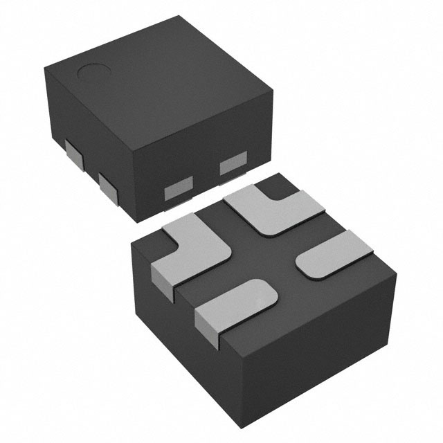
• STDFN 4L, 1.0 x 1.0 x 0.55 mm
SLG5NT1593V
The SLG5NT1593V is designed for load switching applications with ultra low quiescent current. The part comes with one
28.5 mΩ 1.0 A rated P-channel MOSFET controlled by a single
ON control pin. The product is packaged in an ultra-small 1.0
x 1.0 mm package.
4
GND
3
VOUT
4-pin STDFN
(Top View)
Block Diagram
VOUT
VIN
1.0 A
ON
Silego Technology, Inc.
000-005NT1593-10
Fixed Slew
Rate Control
Rev 1.0
Revised September 23, 2014
�SLG5NT1593V
Pin Description
Pin #
Pin Name
Type
Pin Description
1
ON
Input
Turns on MOSFET.
2
VIN
MOSFET
3
VOUT
MOSFET
4
GND
GND
Power MOSFET input
Power MOSFET output
Ground
Ordering Information
Part Number
Type
Production Flow
SLG5NT1593V
STDFN 4L
Industrial, -40 °C to 85 °C
SLG5NT1593VTR
STDFN 4L (Tape and Reel)
Industrial, -40 °C to 85 °C
000-005NT1593-10
Page 2 of 9
�SLG5NT1593V
Absolute Maximum Ratings
Parameter
VDD
TS
ESDHBM
WDIS
Description
Conditions
Min.
Typ.
Max.
Unit
--
--
6
V
-65
--
140
°C
2000
--
--
V
--
--
0.5
W
--
--
1.5
A
Power Supply
Storage Temperature
ESD Protection
Human Body Model
Package Power Dissipation
MOSFET IDSPK Peak Current from Drain to Source For no more than 1 ms with 1% duty cycle
Note: Stresses greater than those listed under “Absolute Maximum Ratings” may cause permanent damage to the device. This is a stress rating
only and functional operation of the device at these or any other conditions above those indicated in the operational sections of this
specification is not implied. Exposure to absolute maximum rating conditions for extended periods may affect reliability.
Electrical Characteristics
TA = -40 °C to 85 °C (unless otherwise stated)
Parameter
VIN
IDD
Description
Power Supply Voltage
Power Supply Current (PIN 2)
Conditions
-40 °C to 85 °C
Min.
--
5.5
V
--
0.02
0.1
μA
when ON = VIN, No load
--
0.05
0.5
μA
0.05
1
μA
Leakage Measured from Pin2 to Pin3 when OFF, VIN = 5.5 V
--
ON Pin Input Leakage
RDSON
IDS
TON_Delay
TTotal_ON
Static Drain to Source
ON Resistance @ TA 85°C
Operating Current
ON pin Delay Time
Total Turn On Time
000-005NT1593-10
Unit
1.5
IDS_LKG
Static Drain to Source
ON Resistance @ TA 25°C
Max.
when OFF, VIN = 5.5 V
ION_LKG
RDSON
Typ.
--
--
0.1
μA
@ 5.5 V
--
28.5
32.0
mΩ
@ 3.3 V
--
36.4
40.0
mΩ
@ 2.5 V
--
44.3
49.0
mΩ
@ 1.8 V
--
60.8
65.0
mΩ
@ 1.5 V
--
77.6
82.0
mΩ
@ 5.5 V
--
34.0
36.0
mΩ
@ 3.3 V
--
43.8
46.0
mΩ
@ 2.5 V
--
53.3
56.0
mΩ
@ 1.8 V
--
72.2
76.0
mΩ
@ 1.5 V
--
90.7
94.0
mΩ
VIN = 1.5 V to 5.5 V
--
--
1.0
A
50% ON to Ramp Begin
VIN = 5 V, VOUT_Cap = 0.1 μF,
RL = 10 Ω
12.0
15.0
18.5
μs
50% ON to Ramp Begin
VIN = 3.3 V, VOUT_Cap = 0.1 μF,
RL = 10 Ω
17.0
22.0
30.0
μs
50% ON to Ramp Begin
VIN = 1.5 V, VOUT_Cap = 0.1 μF,
RL = 10 Ω
44.0
55.0
76.0
μs
50% ON to 90% VOUT
VIN = 5 V, VOUT_Cap = 0.1 μF,
RL = 10 Ω
114
122
134
μs
50% ON to 90% VOUT
VIN = 3.3 V, VOUT_Cap = 0.1 μF,
RL = 10Ω
146
156
176
μs
50% ON to 90% VOUT
VIN = 1.5 V, VOUT_Cap = 0.1 μF,
RL = 10 Ω
292
332
399
μs
Page 3 of 9
�SLG5NT1593V
TA = -40 °C to 85 °C (unless otherwise stated)
Parameter
TRISE
Description
Rise Time
Conditions
Min.
Typ.
Max.
Unit
10% VOUT to 90% VOUT
VIN = 5.0 V, VOUT_Cap = 0.1 μF,
RL = 10 Ω
92
97
107
μs
10% VOUT to 90% VOUT
VIN = 3.3 V, VOUT_Cap = 0.1 μF,
RL = 10 Ω
116
120
131
μs
10% VOUT to 90% VOUT
VIN = 1.5 V, VOUT_Cap = 0.1 μF,
RL = 10 Ω
228
253
296
μs
VIN = 1.5 V to 5.5 V, VOUT = 0.4 V
Input Bias
65
80
400
Ω
RDIS
Discharge Resistance
ON_VIH
Initial Turn On Voltage
0.85
--
VIN
V
ON_VIL
Low Input Voltage on ON pin
-0.3
0
0.3
V
6.2
6.5
7.0
μs
TDelay_OFF
OFF Delay Time
000-005NT1593-10
50% ON to VOUT Fall, VIN = 5 V,
RL =10 Ω
Page 4 of 9
�SLG5NT1593V
VIN vs. Max IDS, Safe Operation Area
Safe Operation Area
VIN vs. Max IDS
8
7
6
5
VIN 4
SOA Boundary
3
2
1
0
0
0.5
1
1.5
2
Max IDS
000-005NT1593-10
Page 5 of 9
�SLG5NT1593V
TTotal_ON, TON_Delay and Slew Rate Measurement
ON
50% ON
50% ON
TOFF_DELAY
90% VOUT
VOUT
90% VOUT
TON_DELAY
10% VOUT
10% VOUT
TRISE
TFALL
TTotal_ON
SLG5NT1593V Layout Suggestion
800
Recommended Land Pattern
210
Unit: μm
410
810
190
Exposed Pad
200
1800
000-005NT1593-10
Page 6 of 9
�SLG5NT1593V
Package Top Marking System Definition
Pin 1 Identifier
000-005NT1593-10
XX
Serial Number
Page 7 of 9
�SLG5NT1593V
Package Drawing and Dimensions
4 Lead STDFN Package 1.0 x 1.0 mm
000-005NT1593-10
Page 8 of 9
�SLG5NT1593V
Tape and Reel Specifications
Max Units
Leader (min)
Nominal
Reel &
Package # of
Package Size
Hub Size
Length
Type
Pins
per Reel per Box
Pockets
[mm]
[mm]
[mm]
STDFN 4L
Green
4
1.0 x 1.0 x 0.55
8000
8000
178 / 60
200
400
Trailer (min)
Pockets
Length
[mm]
Tape
Width
[mm]
200
400
8
Part
Pitch
[mm]
2
Carrier Tape Drawing and Dimensions
Pocket BTM Pocket BTM
Package
Length
Width
Type
STDFN 4L
Green
Pocket
Depth
Index Hole
Pitch
Pocket
Pitch
Index Hole
Diameter
Index Hole Index Hole
to Tape
to Pocket Tape Width
Edge
Center
A0
B0
K0
P0
P1
D0
E
F
W
1.16
1.16
0.63
4
2
1.5
1.75
3.5
8
Refer to EIA-481 specification
Recommended Reflow Soldering Profile
Please see IPC/JEDEC J-STD-020: latest revision for reflow profile based on package volume of 0.55 mm3 (nominal). More
information can be found at www.jedec.org.
000-005NT1593-10
Page 9 of 9
�
很抱歉,暂时无法提供与“SLG5NT1593V”相匹配的价格&库存,您可以联系我们找货
免费人工找货