IS31FL3216A-QFLS3-TR 数据手册
IS31FL3216A
16 CHANNELS LED DRIVER
July 2017
GENERAL DESCRIPTION
FEATURES
The IS31FL3216A is a fun light LED controller with an
audio modulation mode. It can store data of 8 frames
with internal RAM to play small animations
automatically.
IS31FL3216A can sample the input signal to modulate
the intensity of LEDs, or control 8 frames playing by
internal ADC block.
The LED current of each channel can be set in 256
steps by adjusting the PWM duty cycle through an I2C
interface. 8 channels can be used as GPIO ports.
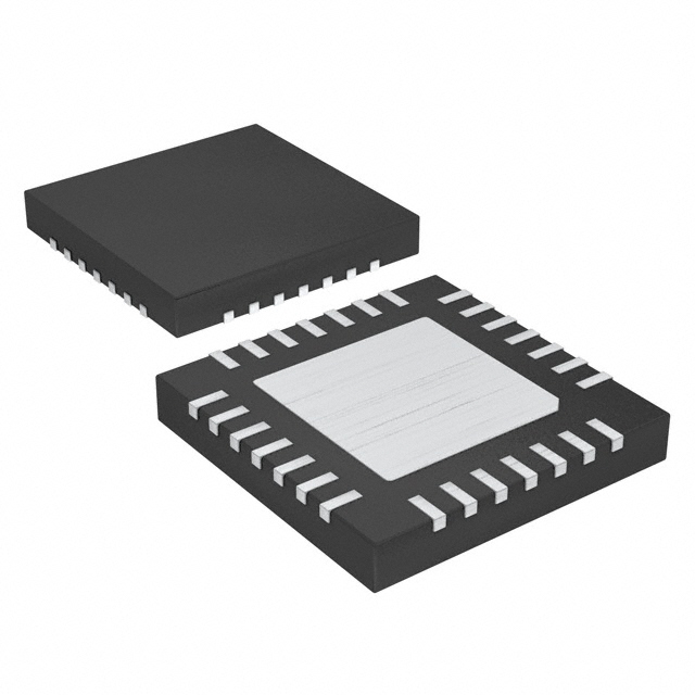
IS31FL3216A is available in QFN-28 (4mm × 4mm). It
operates from 2.7V to 5.5V over the temperature range
of -40°C to +105°C.
APPLICATIONS
Mobile phones and other hand-held devices for
LED display
LED in home appliances
2.7V to 5.5V supply
I2C interface, automatic address increment
function
Internal RAM
Modulate LED brightness with 256 steps PWM
PWM frequency up to 26kHz
Each channel can be controlled independently
Auto Frame Play Mode with 8 frames
8 frames memory for animations
Audio Frame Mode with 8 frames
8 of 16 outputs not used as LED drivers can be
used as GPIO ports
8 levels of maximum intensity control
8kV HBM ESD
Over-temperature protection
-40°C to +105°C temperature range
QFN-28 (4mm × 4mm) package
TYPICAL APPLICATION CIRCUIT
Figure 1
Typical Application Circuit
Note: The IC should be placed far away from the mobile antenna in order to prevent the EMI.
Lumissil Microsystems – www.lumissil.com
Rev. A, 07/03/2017
1
�IS31FL3216A
VBattery
VBattery
1 F
26
OUT1
VCC
OUT2
0.1 F
OUT3
VDD
4.7k
4.7k
OUT4
4.7k
OUT5
24
23
Micro
Controller
21
22
OUT6
SDA
OUT7
SCL
OUT8
INTB
SDB
OUT9
IS31FL3216A OUT10
100k
OUT11
OUT12
0.22 F
2
Audio In
28
27
100k
0.1 F
25
7, 16
IN
OUT13
OUT14
R_EXT
OUT15
C_FILT
OUT16
AD
GND
VBattery
VBattery
3
4
25
5
1 F
VCC
OUT1
AD
OUT2
OUT3
0.1 F
6
OUT4
8
OUT5
9
24
10
23
11
21
12
22
13
OUT6
SDA
OUT7
SCL
OUT8
INTB
SDB
14
OUT9
IS31FL3216A OUT10
OUT11
15
OUT12
0.22 F
17
2
Audio In
18
IN
OUT13
OUT14
19
28
20
27
100k
CLK
26
1
0.1 F
7
16
OUT15
R_EXT
OUT16
C_FILT
GND
CLK
3
4
5
6
8
9
10
11
12
13
14
15
17
18
19
20
1
0
Figure 2
Lumissil Microsystems – www.lumissil.com
Rev. A, 07/03/2017
Typical Application Circuit (Cascade Mode)
2
�IS31FL3216A
PIN CONFIGURATION
Package
Pin Configuration (Top View)
QFN-28
PIN DESCRIPTION
No.
Pin
Description
1
CLK
Clock for chip cascade.
2
IN
Audio signal input.
3~6
OUT1 ~ OUT4
Output channel.
7,16
GND
Ground.
8 ~ 11
OUT5 ~ OUT8
Output channel.
12 ~ 15
OUT9 ~ OUT12
Output channel. Also can be configured as GPIO
port.
17 ~ 20
OUT13 ~ OUT16
Output channel. Also can be configured as GPIO
port.
21
INTB
Interrupt output, active low.
22
SDB
Shutdown, pull to GND in the shutdown mode.
23
SCL
Serial clock input.
24
SDA
Serial data input.
25
AD
I2C address pin.
26
VCC
Power supply.
27
C_FILT
Filter capacitor for audio control.
28
R_EXT
External resistor to regulate the output current.
Thermal Pad
Connect to GND.
Lumissil Microsystems – www.lumissil.com
Rev. A, 07/03/2017
3
�IS31FL3216A
ORDERING INFORMATION
Industrial Range: -40°C to +105°C
Order Part No.
Package
QTY/Reel
IS31FL3216A-QFLS3-TR
QFN-28, Lead-free
2500
Copyright © 2017 Lumissil Microsystems. All rights reserved. Lumissil Microsystems reserves the right to make changes to this specification and its
products at any time without notice. Lumissil Microsystems assumes no liability arising out of the application or use of any information, products or
services described herein. Customers are advised to obtain the latest version of this device specification before relying on any published information and
before placing orders for products.
Lumissil Microsystems does not recommend the use of any of its products in life support applications where the failure or malfunction of the product can
reasonably be expected to cause failure of the life support system or to significantly affect its safety or effectiveness. Products are not authorized for use in
such applications unless Lumissil Microsystems receives written assurance to its satisfaction, that:
a.) the risk of injury or damage has been minimized;
b.) the user assume all such risks; and
c.) potential liability of Lumissil Microsystems is adequately protected under the circumstances
Lumissil Microsystems – www.lumissil.com
Rev. A, 07/03/2017
4
�IS31FL3216A
ABSOLUTE MAXIMUM RATINGS
Supply voltage, VCC
Voltage at any input pin
Current in GND terminal
Maximum junction temperature, TJMAX
Storage temperature range, TSTG
Operating temperature range, TA=TJ
Thermal resistance, θJA
ESD (HBM)
ESD (CDM)
-0.3V ~ +6.0V
-0.3V ~ VCC+0.3V
1A
+150°C
-65°C ~ +150°C
-40°C ~ +105°C
51.4°C /W
±8kV
±1kV
Note: Stresses beyond those listed under “Absolute Maximum Ratings” may cause permanent damage to the device. These are stress ratings
only and functional operation of the device at these or any other condition beyond those indicated in the operational sections of the specifications
is not implied. Exposure to absolute maximum rating conditions for extended periods may affect device reliability.
ELECTRICAL CHARACTERISTICS
TA = 25°C, VCC = 2.7V ~ 5.5V, unless otherwise noted. Typical values are TA = 25°C, VCC = 3.6V.
Symbol
Parameter
Condition
VCC
Supply voltage
ICC
Quiescent power supply current
VSDB = VCC
ISD
Shutdown current
VSDB = 0V or software shutdown
Min.
Typ.
2.7
Max.
Unit
5.5
V
5.2
mA
1
μA
PWM Control Mode, VDS=0.6V
PWM duty cycle=0xFF, 03h=0x70
21
(Note 1)
Audio Frame Mode, VDS=0.6V
VIN = 3Vp-p, 1kHz square wave
Audio gain=0dB
18
(Note 1)
mA
IOUT
Average output current
VHR
Current sink headroom voltage
I
= 20mA
(when use as GPIO output ports) OUT
400
mV
fPWM
PWM frequency of output
26
kHz
Logic Electrical Characteristics (SDB, SDA, SCL, AD, INTB)
VIL
Logic “0” input voltage
VCC = 2.7V
VIH
Logic “1” input voltage
VCC = 5.5V
IIL
Logic “0” input current
VIN = 0V (Note 2,3)
5
nA
IIH
Logic “1” input current
VIN = VCC (Note 2,3)
5
nA
Lumissil Microsystems – www.lumissil.com
Rev. A, 07/03/2017
0.4
1.4
V
V
5
�IS31FL3216A
DIGITAL INPUT SWITCHING CHARACTERISTICS (Note 3)
Symbol
Parameter
Condition
Min.
Typ.
Max.
Unit
400
kHz
fSCL
Serial-Clock frequency
tBUF
Bus free time between a STOP and a START
condition
1.3
μs
tHD, STA
Hold time (repeated) START condition
0.6
μs
tSU, STA
Repeated START condition setup time
0.6
μs
tSU, STO
STOP condition setup time
0.6
μs
tHD, DAT
Data hold time
tSU, DAT
Data setup time
100
ns
tLOW
SCL clock low period
1.3
μs
tHIGH
SCL clock high period
0.7
μs
0.9
μs
tR
Rise time of both SDA and SCL signals,
receiving
(Note 4)
20+0.1Cb
300
ns
tF
Fall time of both SDA and SCL signals,
receiving
(Note 4)
20+0.1Cb
300
ns
Note 1: The average output current of each channel is IOUT.
Note 2: All LEDs are on.
Note 3: Guaranteed by design.
Note 4: Cb = total capacitance of one bus line in pF. ISINK≤ 6mA. tR and tF measured between 0.3×VCC and 0.7×VCC.
Lumissil Microsystems – www.lumissil.com
Rev. A, 07/03/2017
6
�IS31FL3216A
DETAILED DESCRIPTION
I2C INTERFACE
The IS31FL3216A uses a serial bus, which conforms to
the I2C protocol, to control the chip’s functions with two
wires: SCL and SDA. The IS31FL3216A has a 7-bit
slave address (A7:A1), followed by the R/W bit, A0.
Set A0 to “0” for a write command and set A0 to “1” for a
read command. The value of bits A1 and A2 are
decided by the connection of the AD pin.
The complete slave address is:
Table 1 Slave Address
Bit
A7:A3
A2:A1
A0
Value
11101
AD
1/0
AD connected to GND, AD = 00;
AD connected to VCC, AD = 11;
AD connected to SCL, AD = 01;
AD connected to SDA, AD = 10;
Following acknowledge of IS31FL3216A, the register
address byte is sent, most significant bit first.
IS31FL3216A must generate another acknowledge
indicating that the register address has been received.
Then 8-bit of data byte are sent next, most significant
bit first. Each data bit should be valid while the SCL
level is stable high. After the data byte is sent, the
IS31FL3216A must generate another acknowledge to
indicate that the data was received.
The “STOP” signal ends the transfer. To signal “STOP”,
the SDA signal goes high while the SCL signal is high.
ADDRESS AUTO INCREMENT
The SCL line is uni-directional. The SDA line is
bi-directional (open-collector) with a pull-up resistor
(typically 4.7kΩ). The maximum clock frequency
specified by the I2C standard is 400kHz. In this
discussion, the master is the microcontroller and the
slave is the IS31FL3216A.
The timing diagram for the I2C is shown in Figure 3.
The SDA is latched in on the stable high level of the
SCL. When there is no interface activity, the SDA line
should be held high.
The “START” signal is generated by lowering the SDA
signal while the SCL signal is high. The start signal will
alert all devices attached to the I2C bus to check the
incoming address against their own chip address.
The 8-bit chip address is sent next, most significant bit
first. Each address bit must be stable while the SCL
level is high.
After the last bit of the chip address is sent, the master
checks for the IS31FL3216A’s acknowledge. The
master releases the SDA line high (through a pull-up
Figure 3
Lumissil Microsystems – www.lumissil.com
Rev. A, 07/03/2017
resistor). Then the master sends an SCL pulse. If the
IS31FL3216A has received the address correctly, then
it holds the SDA line low during the SCL pulse. If the
SDA line is not low, then the master should send a
“STOP” signal (discussed later) and abort the transfer.
To write multiple bytes of data into IS31FL3216A, load
the address of the data register that the first data byte
is intended for. During the IS31FL3216A acknowledge
of receiving the data byte, the internal address pointer
will increment by one. The next data byte sent to
IS31FL3216A will be placed in the new address, and
so on. The auto increment of the address will continue
as long as data continues to be written to IS31FL3216A
(Figure 6).
READING PORT REGISTERS
To read the device data, the bus master must first send
____
the IS31FL3216A address with the R/W bit set to “0”,
followed by the command byte, which determines
which register is accessed. After a restart, the bus
master must then send the IS31FL3216A address with
____
the R/W bit set to “1”. Data from the register defined
by the command byte is then sent from the
IS31FL3216A to the master (Figure 7).
Interface timing
7
�IS31FL3216A
Figure 4
Figure 5
Figure 6
Bit transfer
Writing to IS31FL3216A (Typical)
Writing to IS31FL3216A (Automatic Address Increment)
Figure 7
Lumissil Microsystems – www.lumissil.com
Rev. A, 07/03/2017
Reading from IS31FL3216A
8
�IS31FL3216A
REGISTER DEFINITION
Table 2 Register Function
Address
00h
Name
Configuration Register
01h
LED Control Register
02h
Function
Table
R/W
Default
Set the operating mode of IS31FL3216A
3
W
1000 0000
OUT9~OUT16 enable bit
4
W
OUT1~OUT8 enable bit
5
W
1111 1111
03h
Lighting Effect Register
Set the output current and the audio gain
6
W
04h
Channel Configuration
Register
Set the operating mode of OUT9~OUT16
7
W
05h
GPIO Configuration Register
Set the operating mode of OUT9~OUT16
as the GPIO port
8
W
06h
Output Port Register
Set the logic level of OUT9~OUT16 as
the output port
9
W
07h
Interrupt Control Register
Set the interrupt function of
OUT9~OUT16
10
W
08h
State Register
Store the state of OUT9~OUT16 as the
input port
11
R
09h
ADC Sample Rate Register
Set the ADC sample rate of the input
signal
12
W
10h~1Fh PWM Register
Set the PWM duty cycle data
13
W
20h~AFh Frame Register
Store the data of 8 frames
14
W
-
-
W
xxxx xxxx
B0h
Update Register
Load PWM Register data
B6h
Frame Delay Register
Set the delay time between each frame
15
W
B7h
Frame Start Register
Set the start frame in Auto Frame Play
Mode
16
W
Table 3 00h Configuration Register
xxxx xxxx
0000 0000
0000 0000
Table 4 01h LED Control Register (OUT9~OUT16)
Bit
D7
D6:D5
D4
D3:D0
Bit
D7:D0
Name
SSD
MODE
AE
-
Name
OUT16:OUT9
Default
1
00
0
0000
Default
1111 1111
The Configuration Register sets the operating mode of
IS31FL3216A.
SSD
0
1
Software Shutdown Enable
Normal operation
Software shutdown mode
MODE
00
01
10
11
Operation Mode Selection
PWM Control Mode
Auto Frame Play Mode
Audio Frame Mode
Not available
AE
0
1
Audio Modulated Enable
Output current is set by register
Output current is modulated by audio signal
Lumissil Microsystems – www.lumissil.com
Rev. A, 07/03/2017
0000 0000
Table 5 02h LED Control Register (OUT1~OUT8)
Bit
D7:D0
Name
OUT8:OUT1
Default
1111 1111
The LED Control Registers store the on or off state of
each channel.
OUTx
0
1
LED State
LED off
LED on
9
�IS31FL3216A
Table 6 03h Lighting Effect Register
Bit
D7
D6:D4
D3
D2:D0
Name
CM
CS
AGCE
AGS
Default
0
000
0
000
The Lighting Effect Register sets the output current and
the audio gain.
Table 8 05h GPIO Configuration Register
(OUT9~OUT16)
Bit
D7:D0
Name
OUT16:OUT9
Default
0000 0000
Set the state of OUT9~OUT16 as the GPIO port.
CM
0
1
Chip Cascade Mode
Master Mode
Slave Mode
OUTx
0
1
CS
000
001
010
011
100
101
110
111
Output Current Selection
ILED × 1.0
ILED × 0.75
ILED × 0.5
ILED × 0.25
ILED × 2.0
ILED × 1.75
ILED × 1.5
ILED × 1.25
Table 9 06h Output Configuration Register
(OUT9~OUT16)
The ILED is set by the resistor REXT. Please refer to
Page 14 for detail information.
GPIO Configuration
Output port
Input port
Bit
D7:D0
Name
OUT16:OUT9
Default
0000 0000
Set the logic level of OUT9~OUT16 as the output port.
Output State
Output low
Output high
OUTx
0
1
Table 10 07h Interrupt Control Register
(OUT9~OUT16)
AGCE
0
1
AGC Enable
Enable
Disable
AGS
000
001
010
011
100
101
110
111
Audio Gain Selection
0dB
3dB
6dB
9dB
12dB
15dB
18dB
21dB
Bit
D7:D0
Name
OUT16:OUT9
Default
0000 0000
Set the interrupt function of OUT9~OUT16 as the input
port.
Interrupt Function Enable
Enable
Disable
OUTx
0
1
Table 7 04h Channel Configuration Register
(OUT9~OUT16)
Table 11 08h State Register (OUT9~OUT16)
Bit
D7:D0
Bit
D7:D0
Name
OUT16:OUT9
Name
OUT16:OUT9
Default
xxxx xxxx
Default
0000 0000
Configure the operating mode of OUT9~OUT16. If any
port is set as GPIO, the Lighting Effect Register will be
unavailable for the port.
OUTx
0
1
Store the input state of OUT9~OUT16 as the input port
(Write only). The INTB pin will be pulled high until the
MCU reads the data of State Register.
Channel Configuration
LED output
GPIO port
Lumissil Microsystems – www.lumissil.com
Rev. A, 07/03/2017
10
�IS31FL3216A
Table 12 09h ADC Sample Rate Register
Bit
D7:D0
Name
SR
Default
0000 0000
The value of ADC Sample Rate Register decides the
sample rate of ADC for Audio Frame Mode. The sample
rate could be computed using the Formula (1):
7
SR 100kHz / D[n] 2 n
(1)
n 0
Where “n” indicates the bit location in the respective
ADC Sample Rate Register.
For example: D7:D0 = 10110100
SR = 100kHz/(22+24+25+27)
= 556Hz
Table 13 10h~1Fh PWM Register (OUT16~OUT1)
Bit
D7:D0
Name
PWM
Default
0000 0000
The PWM Registers adjusts LED luminous intensity in
256 steps.
The value of a channel’s PWM Register decides the
average output current for each output, OUT1~OUT16.
The average output current may be computed using the
Formula (2):
I OUT
I MAX 7
D[n] 2 n
256 n0
(2)
Where “n” indicates the bit location in the respective
PWM Registers.
For example: D7:D0 = 10110101
IOUT = IMAX (20+22+24+25+27)/256
IMAX is set by the CS bit of Lighting Effect Register
(03h).
Table 14 20h~AFh Frame Register Address List
Frame
LED Control Register
PWM Register
Frame 1
20h ~ 21h
22h ~ 31h
Frame 2
32h ~ 33h
34h ~ 43h
Frame 3
44h ~ 45h
46h ~ 55h
Frame 4
56h ~ 57h
58h ~ 67h
Frame 5
68h ~ 69h
6Ah ~ 79h
Frame 6
7Ah ~ 7Bh
7Ch ~ 8Bh
Frame 7
8Ch ~ 8Dh
8Eh ~ 9Dh
Frame 8
9Eh ~ 9Fh
A0h ~ AFh
Lumissil Microsystems – www.lumissil.com
Rev. A, 07/03/2017
Frame Registers store the data of 8 frames. Each
frame is controlled by two LED Control Registers and
sixteen PWM Registers.
The detail about the LED Control Register is shown in
Table 4, 5 and the PWM Register is shown in Table 13.
B0h Update Register
The data sent to the PWM Register will be stored in
temporary registers. A write operation of “0000 0000”
to the Update Register is required to update the
registers.
Table 15 B6h Frame Delay Register
Bit
D7:D5
D4:D0
Name
FDT
-
Default
000
00000
Set the delay time between each frame in Auto Frame
Play Mode.
Frame Delay Time
4.87ms
9.5ms
19ms
38ms
76ms
152ms
304ms
608ms
FDT
000
001
010
011
100
101
110
111
Table 16 B7h Frame Start Register
Bit
D7:D5
D4:D0
Name
FS
-
Default
000
00000
Set the start frame in Auto Frame Play Mode.
FS
000
001
010
011
100
101
110
111
Frame Start
Frame 1
Frame 2
Frame 3
Frame 4
Frame 5
Frame 6
Frame 7
Frame 8
For example, if FS bit sets to “011”, it plays from the
fourth frame to the eighth frame then cycled back to
the first frame.
11
�IS31FL3216A
FUNCTIONAL BLOCK DIAGRAM
C_FILT
VCC
IN
Current
Control Block
ADC
I2C
Interface
Configuration
Register
SYNC
Decoder
CLK
R_EXT
SCL
SDA
AD
Frame
Control
Frame Data
Registers
OUT1 ~ OUT8
SDB
Shutdown
Control
PWM Registers
INTB
OUT9 ~ OUT16
GPIO Port
Registers
INT
BIAS
PWM
Counter
Band-gap
Lumissil Microsystems – www.lumissil.com
Rev. A, 07/03/2017
OSC
GND
12
�IS31FL3216A
APPLICATION INFORMATION
PWM CONTROL
By setting the MODE bit of the Configuration Register
(00h) to “00”, IS31FL3216A operates in PWM Control
Mode. The LED brightness of 16 channels can be
modulated with 256 steps by PWM Registers. For
example, if the data in PWM Register is “0000 0100”,
then the PWM is the fourth step.
Writing new data continuously to the registers can
modulate the brightness of the LEDs to achieve a
breathing effect.
GAMMA CORRECTION
In order to perform a better visual LED breathing effect
we recommend using a gamma corrected PWM value
to set the LED intensity. This results in a reduced
number of steps for the LED intensity setting, but
causes the change in intensity to appear more linear to
the human eye.
Gamma correction, also known as gamma
compression or encoding, is used to encode linear
luminance to match the non-linear characteristics of
display. Since the IS31FL3216A can modulate the
brightness of the LEDs with 256 steps, a gamma
correction function can be applied when computing
each subsequent LED intensity setting such that the
changes in brightness matches the human eye's
brightness curve.
Table 17 32 Gamma Steps With 256 PWM Steps
Choosing more gamma steps provides for a more
continuous looking breathing effect. This is useful for
very long breathing cycles. The recommended
configuration is defined by the breath cycle T. When
T=1s, choose 32 gamma steps, when T=2s, choose
64 gamma steps. The user must decide the final
number of gamma steps not only by the LED itself, but
also based on the visual performance of the finished
product.
Table 18 64 Gamma Steps With 256 PWM Steps
C(0)
C(1)
C(2)
C(3)
C(4)
C(5)
C(6)
C(7)
0
1
2
3
4
5
6
7
C(8)
C(9)
C(10)
C(11)
C(12)
C(13)
C(14)
C(15)
8
10
12
14
16
18
20
22
C(16)
C(17)
C(18)
C(19)
C(20)
C(21)
C(22)
C(23)
24
26
29
32
35
38
41
44
C(24)
C(25)
C(26)
C(27)
C(28)
C(29)
C(30)
C(31)
47
50
53
57
61
65
69
73
C(32)
C(33)
C(34)
C(35)
C(36)
C(37)
C(38)
C(39)
77
81
85
89
94
99
104
109
C(40)
C(41)
C(42)
C(43)
C(44)
C(45)
C(46)
C(47)
114
119
124
129
134
140
146
152
C(48)
C(49)
C(50)
C(51)
C(52)
C(53)
C(54)
C(55)
158
164
170
176
182
188
195
202
C(56)
C(57)
C(58)
C(59)
C(60)
C(61)
C(62)
C(63)
209
216
223
230
237
244
251
255
C(1)
C(2)
C(3)
C(4)
C(5)
C(6)
C(7)
0
1
2
4
6
10
13
18
256
C(8)
C(9)
C(10)
C(11)
C(12)
C(13)
C(14)
C(15)
224
22
28
33
39
46
53
61
69
192
C(16)
C(17)
C(18)
C(19)
C(20)
C(21)
C(22)
C(23)
78
86
96
106
116
126
138
149
C(24)
C(25)
C(26)
C(27)
C(28)
C(29)
C(30)
C(31)
161
173
186
199
212
226
240
255
256
PWM Data
C(0)
160
128
96
64
32
224
0
0
8
PWM Data
192
16
24
32
40
48
56
64
Intensity Steps
160
Figure 9
128
Gamma Correction (64 Steps)
Note, the data of 32 gamma steps is the standard value and the data
of 64 gamma steps is the recommended value.
96
64
32
0
0
4
8
12
16
20
24
28
32
Intensity Steps
Figure 8
Gamma Correction (32 Steps)
Lumissil Microsystems – www.lumissil.com
Rev. A, 07/03/2017
13
�IS31FL3216A
AUTO FRAME PLAY MODE
AUDIO FRAME MODE
By setting the MODE bit of the Configuration Register
(00h) to “10”, the IS31FL3216A operates in Audio
Frame Mode. It stores data of 8 frames and the 8
frames playing follow the input signal. 09h register is
used to set the ADC sample rate for the input signal to
control frames playing. It plays the first frame when the
value is the smallest and plays the eighth frame when
the value is the biggest (See Table 14).
AUDIO MODULATED MODE AND GAIN SETTING
By setting the AE bit of the Configuration Register (00h)
to “1”, IS31FL3216A operates in Audio Modulated
Mode. The intensity of LEDs is adjusted by the input
signal. The audio input gain can be set by the Lighting
Effect Register (03h).
CHANNEL MODE SETTING
IS31FL3216A has 16 channels for LEDs output.
OUT9~OUT16 also can be set as GPIO ports. By
setting the OUTx bit of the Channel Configuration
Register (04h) to “1”, the corresponding channel will be
used as GPIO port. When the OUTx is set to “0”, the
corresponding channel will be used as LED output.
CASCADE FOR SYNCHRONIZATION OF CHIPS
Operating in the cascade mode can make two chips
synchronize. By setting the CM bit of the Lighting Effect
Register (03h) to “0”, IS31FL3216A operates as a
master. The CLK pin offers the output clock signal.
When the CM bit sets to “1”, IS31FL3216A operates as
a slave. The CLK pin as a clock input pin. If there is only
one chip to use, setting CM bit to “0” and the CLK pin
should be floating.
INTERRUPT FUNCTION
When OUT9~OUT16 configure as input port and the
interrupt function enabled, the INTB pin is available. If
any input port of OUT9~OUT16 has state changing, the
INTB pin will be pulled low. The MCU can get the
information via reading the State Register (08h). The
INTB will be back to high until the MCU reading the
State Register (08h).
REXT
The output current of each LED channel can be
adjusted by the external resistor on pin 28, REXT, as
described in Formula (3).
Lumissil Microsystems – www.lumissil.com
Rev. A, 07/03/2017
1 .2
1400
REXT [k]
(3)
For example, in Figure 1, REXT = 100kΩ,
So I LED
1 .2
1400 16.8mA
100
The recommended minimum value of REXT is
100kΩ. Smaller REXT values will result in a per channel
current whose total will exceed the absolute maximum
package current rating causing thermal damage to the
device.
The ILED defines the IMAX value which is set by the CS
bit of Lighting Effect Register (03h). And the average
output current of each output, IOUT, is calculated by the
IMAX and PWM Register as Formula (2) in Table 13.
PWM FREQUENCY
The IS31FL3216A output channels operate with a
default PWM frequency of 26kHz. Because all the
OUTx channels are synchronized, the DC supply will
experience large instantaneous current surges when
the OUTx channels turn ON. These current surges will
generate an AC ripple on the power supply which
cause stress to the decoupling capacitors.
When the AC ripple is applied to a monolithic ceramic
capacitor chip (MLCC) it will expand and contract
causing the PCB to flex and generate audible hum in
the range of between 20Hz to 20kHz. To avoid this
hum, there are many countermeasures, such as
selecting the capacitor type and value which will not
cause the PCB to flex and contract.
Figure 10 below shows the variation of output PWM
frequency across supply voltage and temperature.
40
Output PWM Frequency (kHz)
By setting the MODE bit of the Configuration Register
(00h) to “01”, the IS31FL3216A operates in Auto Frame
Play Mode. It stores data of 8 frames and automatically
plays in order. Customers can configure the delay time
between each two frames and the first playing frame by
setting the Frame Delay Register (B6h) and the Frame
Start Register (B7h).
I LED [mA]
125°C
30
85°C
25°C
20
-40°C
10
2.5
3
3.5
4
4.5
5
5.5
VCC (V)
Figure 10
VCC vs. Output PWM Frequency
SHUTDOWN MODE
Shutdown mode can either be used as a means of
reducing power. During shutdown mode all registers
14
�IS31FL3216A
retain their data and OUT9~OUT16 still can be
available as GPIO port.
Software Shutdown
By setting SSD bit of the Configuration Register (00h) to
“1”, the IS31FL3216A will operate in software shutdown
mode, wherein they consume only 1μA (Typ.) current.
When the IS31FL3216A is in software shutdown mode,
all current sources are switched off.
Hardware Shutdown
The chip enters hardware shutdown mode when the
SDB pin is pulled low.
Lumissil Microsystems – www.lumissil.com
Rev. A, 07/03/2017
15
�IS31FL3216A
CLASSIFICATION REFLOW PROFILES
Profile Feature
Pb-Free Assembly
Preheat & Soak
Temperature min (Tsmin)
Temperature max (Tsmax)
Time (Tsmin to Tsmax) (ts)
150°C
200°C
60-120 seconds
Average ramp-up rate (Tsmax to Tp)
3°C/second max.
Liquidous temperature (TL)
Time at liquidous (tL)
217°C
60-150 seconds
Peak package body temperature (Tp)*
Max 260°C
Time (tp)** within 5°C of the specified
classification temperature (Tc)
Max 30 seconds
Average ramp-down rate (Tp to Tsmax)
6°C/second max.
Time 25°C to peak temperature
8 minutes max.
Figure 11
Classification profile
Lumissil Microsystems – www.lumissil.com
Rev. A, 07/03/2017
16
�IS31FL3216A
PACKAGE INFORMATION
QFN-28
Lumissil Microsystems – www.lumissil.com
Rev. A, 07/03/2017
17
�IS31FL3216A
RECOMMENDED LAND PATTERN
Note:
1. Land pattern complies to IPC-7351.
2. All dimensions in MM.
3. This document (including dimensions, notes & specs) is a recommendation based on typical circuit board manufacturing parameters. Since
land pattern design depends on many factors unknown (eg. user’s board manufacturing specs), user must determine suitability for use.
Lumissil Microsystems – www.lumissil.com
Rev. A, 07/03/2017
18
�IS31FL3216A
REVISION HISTORY
Revision
A
Detail Information
Initial release
Lumissil Microsystems – www.lumissil.com
Rev. A, 07/03/2017
Date
2017.07.03
19
�