IS31LT3117
53V, 350MA, 4-CHANNEL CONSTANT CURRENT REGULATOR WITH OTP
July 2021
GENERAL DESCRIPTION
FEATURES
The IS31LT3117 is a 4-channel, linear regulated,
constant current LED driver which can provide 4 equal
currents outputs of up to 350mA per channel to drive
high brightness LEDs over an input voltage range of
6V to 53V, while maintaining an output leakage current
of less than 1µA. The output current is easily
programmed using a single, tiny external resistor. The
outputs of the IS31LT3117 can be connected in
parallel to allow greater than 350mA output current.
The IS31LT3117 also features a PWM input to enable
simple dimming control using a digital control signal.
The recommended frequency range of the PWM signal
is 4kHz ~ 100kHz.
APPLICATIONS
The IS31LT3117 provides a unique over temperature
protection scheme. A hard shutdown which turns off all
LED currents occurs if the die junction temperature
exceeds the maximum value of 160°C. However, as
the die junction temperature rises up to over 130°C
(Typ.), the output current will begin to roll off at a rate
of -2.22%/°C (Typ.). If the die temperature continues to
rise above the hard shutdown temperature threshold,
the LED currents will drop to zero. When temperature
returns to 140°C (Typ.) or below, the hard shutdown
protection is released and the chip will function again.
6V to 53V input supply voltage range
Up to 1.4A total output current
Over temperature protections
Thermal current regulation above 130°C
±3% output current matching between channels
PWM dimming and shutdown control input
Optional 2.5V output to drive external standoff BJTs
Very few external components
Industrial LED lighting
Low EMI lighting applications
Low-side constant current regulator
The IS31LT3117 also has an optional 2.5V reference
voltage output which is able to supply up to 10mA (typ.)
output current. This voltage may be used to drive the
base of the external BJTs for higher current
applications in such case, driving for a wide varying
input voltage is needed.
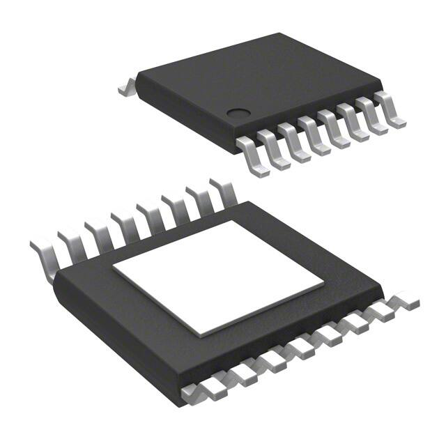
The IS31LT3117 is offered in eTSSOP-16 package
with operating temperature range of -40°C to +125°C.
TYPICAL APPLICATION CIRCUIT
Figure 1
Lumissil Microsystems – www.lumissil.com
Rev. C, 07/15/2021
IS31LT3117 Directly Driving 4 LED Strings
1
�IS31LT3117
VCC
6V ~ 53VDC
COUT
33µF
R5
3
8
VCC
CIN
10µF
RISET
GND
VLED1
PGND
VLED2
VLED3
PWM
Q5
Vb
1µF
IS31LT3117
6
CPWM
1nF 1
RPWM
1kΩ
9
ISET
2,5
PWM
VREF
VLED4
16
14
Q1
R1
100nF
Vb
Q2
R2
Vb
Q3
100nF
R3
100nF
Vb
Q4
R4
Vb
100nF
12
10
Optional
Figure 2
IS31LT3117 With Optional 2.5V Output Driving 4 External Standoff BJTs
Note 1: The 33µF output capacitor should be placed as close to the LED array as possible in order to minimize the parasitic inductor effect due
to the output wiring.
Note 2: The resistor RISET should be place as close to ISET and GND pins as possible.
Note 3: If you want less than four channels, the unused channel should be connected to GND.
Note 4: RPWM and CPWM are optional to optimize PWM pin ESD performance. But a RC filter will degrade PWM dimming contrast ratio.
Lumissil Microsystems – www.lumissil.com
Rev. C, 07/15/2021
2
�IS31LT3117
PIN CONFIGURATION
Package
Pin Configuration (Top View)
eTSSOP-16
PIN DESCRIPTION
No.
Pin
Description
1
PWM
PWM control pin. (PWM=high, enable. PWM=low
for 3.5ms, disable)
2, 5
PGND
Power ground.
3
VCC
Voltage supply input (6V~53V).
4,7,11,13,15
NC
No connection.
6
GND
Ground.
8
ISET
A resistor from this pin to ground will set all the
channel sink currents to the same value.
9
VREF
2.5V reference output capable of sourcing 10mA
(Typ.). A 1µF capacitor must be connected from this
pin to ground.
10,12,14,16
VLED4~VLED1
Current source outputs. Each channel should be
connected to GND if it is not used.
Thermal Pad
Connect to ground.
Lumissil Microsystems – www.lumissil.com
Rev. C, 07/15/2021
3
�IS31LT3117
ORDERING INFORMATION
Industrial Range: -40°C to +125°C
Order Part No.
Package
QTY
IS31LT3117-ZLS4-TR
IS31LT3117-ZLS4
eTSSOP-16, Lead-free
2500/Reel
96/Tube
Copyright © 2021 Lumissil Microsystems. All rights reserved. Lumissil Microsystems reserves the right to make changes to this specification and its
products at any time without notice. Lumissil Microsystems assumes no liability arising out of the application or use of any information, products or
services described herein. Customers are advised to obtain the latest version of this device specification before relying on any published information and
before placing orders for products.
Lumissil Microsystems does not recommend the use of any of its products in life support applications where the failure or malfunction of the product can
reasonably be expected to cause failure of the life support system or to significantly affect its safety or effectiveness. Products are not authorized for use in
such applications unless Lumissil Microsystems receives written assurance to its satisfaction, that:
a.) the risk of injury or damage has been minimized;
b.) the user assume all such risks; and
c.) potential liability of Lumissil Microsystems is adequately protected under the circumstances
Lumissil Microsystems – www.lumissil.com
Rev. C, 07/15/2021
4
�IS31LT3117
ABSOLUTE MAXIMUM RATINGS (NOTE 4)
VCC pin to GND
Voltage at PWM and VLEDx pins
Voltage at ISET pin
Current at VREF pin
Junction temperature, TJ
Storage temperature range, TSTG
Operating temperature range, TA
Power dissipation, PD(MAX) (Note 5)
Thermal resistance, junction to ambient, still air, θJA
ESD (HBM)
ESD (CDM)
-0.3V ~ +56V
-0.3V ~ +56V
-0.3V ~ +6.0V
10mA
-40°C ~ +160°C
-65°C ~ +150°C
-40°C ~ +125°C
2.5W
39.9°C/W
All pins pass 2kV, except all ground pin pass 1kV
All pins pass 750V, except Pin 1 passes 100V
Note 4: Stresses beyond those listed under “Absolute Maximum Ratings” may cause permanent damage to the device. These are stress ratings
only and functional operation of the device at these or any other condition beyond those indicated in the operational sections of the specifications
is not implied. Exposure to absolute maximum rating conditions for extended periods may affect device reliability.
Note 5: Detail information please refers to package thermal de-rating curve on Page 13.
ELECTRICAL CHARACTERISTICS
Valid are at VCC = 12V, TA = TJ = -40°C ~ +125°C, typical value at 25°C, unless otherwise noted.
Symbol
Parameter
Conditions
Min.
Typ.
Max.
Unit
VCC
Supply voltage range
6.0
53
V
RISET
The ISET resistance
5.8
203
kΩ
ISINK
Output current per channel
367.5
mA
IIN
Quiescent Input supply current
ISD
Shutdown input current
tSD
The time of PWM pin keeping low
to shutdown the IC
RISET= 5.8kΩ, PWM= High
VVLEDx= 1V, TA= 25°C
332.5
350
RISET= 5.8kΩ, PWM= High
13.8
RISET= 203kΩ, PWM= High
6.3
PWM= Low, VCC= 12V
90
3.5
mA
µA
ms
fPWM
The PWM dimming frequency
VCC= 12V (Note 8)
VHR
Recommended VLED output
voltage headroom
ISINK= 350mA (Note 6)
ILEAKAGE
Leakage current per channel
PWM= Low, VVLEDx= 53V
tRISE
Output current rise time
RISET=5.8kΩ, PWM=20kHz,
current rise from 10%~90%
(Note 7)
300
ns
tFALL
Output current fall time
RISET=5.8kΩ, PWM=20kHz,
current fall down from
90%~10% (Note 7)
200
ns
VISET
ISET pin output voltage
PWM pin input logic high voltage
VPWM rising
VPWML
PWM pin input logic low voltage
VPWM falling
100
0.8
kHz
V
1
1.16
VPWMH
Lumissil Microsystems – www.lumissil.com
Rev. C, 07/15/2021
4
1.27
1.38
1.4
µA
V
V
0.4
V
5
�IS31LT3117
ELECTRICAL CHARACTERISTICS (CONTINUE)
Valid are at VCC = 12V, TA = TJ = -40°C ~ +125°C, typical value at 25°C, unless otherwise noted.
Symbol
Parameter
Conditions
Min.
Typ.
Max.
Unit
TRO
Thermal roll off threshold
(Note 7)
130
°C
TSD
Thermal shutdown threshold
Temperature rising (Note 7)
160
°C
TSD-HYS
Thermal shutdown hysteresis
Temperature falling (Note 7)
20
°C
ΔISINK/ISINK
Current matching between
Channels
RISET= 5.8kΩ, PWM= High
VVLEDx= 1V
VREF
Reference voltage output
-3
2.32
2.5
3
%
2.76
V
Note 6: It is a recommended value to ensure a better line regulation of 350mA output current.
Note 7: Guarantee by design.
Note 8: If add RC network on the PWM pin, the PWM dimming contrast ratio will be degraded and the recommended maximum PWM frequency
is 50kHz.
Lumissil Microsystems – www.lumissil.com
Rev. C, 07/15/2021
6
�IS31LT3117
TYPICAL PERFORMANCE CHARACTERISTICS
1.30
9.0
TA = 25ºC
VCC = 12V
1.28
8.8
8.7
8.6
VISET (V)
Supply Current (mA)
8.9
8.5
8.4
1.26
1.24
8.3
8.2
1.22
8.1
8.0
6
12
18
24
30
36
42
48
1.20
-40
54
-25
-10
5
Supply Voltage (V)
Figure 3
35
50
65
80
95
110 125
Temperature (°C)
Supply Current vs. Supply Voltage
Figure 4
12
VISET vs. Temperature
2.60
TA = 25ºC
VCC = 12V
2.58
11
2.56
10
VREF (V)
Supply Current (mA)
20
9
8
2.52
2.50
7
6
-40
2.54
2.48
2.46
-25
-10
5
20
35
50
65
80
95
110 125
6
12
18
36
42
54
48
Supply Voltage (V)
Temperature (°C)
Figure 5
30
24
Figure 6
Supply Current vs. Temperature
VREF vs. Supply Voltage
2.70
1.30
VCC = 12V
TA = 25ºC
2.65
1.28
VREF (V)
VISET (V)
2.60
1.26
1.24
2.55
2.50
1.22
1.20
2.45
6
12
18
24
30
36
42
48
54
60
2.40
-40
-25
-10
5
VISET vs. Supply Voltage
Lumissil Microsystems – www.lumissil.com
Rev. C, 07/15/2021
35
50
65
80
95
110 125
Temperature (°C)
Supply Voltage (V)
Figure 7
20
Figure 8
VREF vs. Temperature
7
�IS31LT3117
400
350
VCC = 12V
300
VCC = 12V
TA = 25ºC
RISET = 5.8kΩ
300
250
200
150
RISET = 20kΩ
Output Current (mA)
Output Current (mA)
350
100
0
0
200
400
600
800
200
150
100
50
RISET = 200kΩ
50
250
0
1000 1200 1400 1600 1800 2000
0
50
100
VVLEDX (mV)
Figure 9
200
RISET (kΩ)
Output Current vs. VVLEDX
Figure 10
400
Output Current vs. RISET
400
VCC = 12V
RISET = 5.8kΩ
fPWM = 4kHz,20kHz,100kHz
380
Output Current (mA)
350
Output Current (mA)
150
300
250
200
150
100
VCC = 12V
3 LEDs
360
340
320
300
280
260
240
50
0
220
0
20
40
60
80
100
200
-40
-25
-10
PWM Duty Cycle (%)
Figure 11
Figure 13
Output Current vs. PWM Duty Cycle
Output Current vs. VPWM on Rising Time
Lumissil Microsystems – www.lumissil.com
Rev. C, 07/15/2021
5
20
35
50
65
80
95
110 125
Temperature (°C)
Figure 12
Figure 14
Output Current vs. Temperature
Output Current vs. VPWM on Falling Time
8
�IS31LT3117
FUNCTIONAL BLOCK DIAGRAM
Lumissil Microsystems – www.lumissil.com
Rev. C, 07/15/2021
9
�IS31LT3117
APPLICATION INFORMATION
FUNCTIONAL DESCRIPTION
IS31LT3117 is a linear current regulator designed to
drive high brightness LEDs. The device integrates 4
channels capable of driving up to 350mA in each
channel and operates over a supply voltage range of
6V to 53V. Output current is easily programmed by
using a single resistor.
The IS31LT3117 incorporates a special thermal
regulation protection feature which prevents the die
temperature from exceeding the maximum rated
junction temperature of 160°C.
IS31LT3117 features a PWM/enable input which can
be used to realize PWM dimming of the LEDs. In
addition, the enable input can be used to put the
device into a low power consumption shutdown mode.
In shutdown, the device consumes only 80µA of supply
current.
VCC
The VCC input pin provides power to the internal
circuitry of the entire chip. The device supply current
will vary with the output current setting due to the
internal reference currents generated for each channel.
The nominal supply current is 11.5mA (RISET=5.8kΩ)
during operation.
ISET
sequence with the same initial propagation delay
(typical 60ns) and interval delay time tINTDEL (typical
200ns). “First On First Off” ensures all channels are of
the same pulse width as the input PWM signal.
PWM
IVLED1
IVLED2
IVLED3
IVLED4
tPG
Figure 15
tINTDEL
tPG
tINTDEL
PWM Dimming Sequential On/Off
Note: there is a propagation time tPG from PWM rising/falling edge to
the first channel activity, typical 60ns.
GND
Signal ground current return pin.
PGND
Power ground current return pin. This pin should be
connected to as large as possible of a copper pad on
the PCB to allow the best possible thermal
performance of the circuit.
The output current for the IS31LT3117 is set by
connecting a resistor from the ISET pin to GND. An
internal 1.27V reference voltage source will supply a
current to the external current setting resistor. The
reference current is internally amplified by a gain of
1600 to each of the 4 outputs. In order to have an
accurate current output, this current setting resistor
must be mounted as close to ISET and AGND pins as
possible.
It is recommended to maintain above a 0.8V VVLEDx to
ensure a better line regulation of 350mA output
current.
PWM
OUTPUT CURRENT
When the PWM input pin is at low state (VPWM < 0.4V)
and stays low for more than 3.5ms, the IS31LT3117
enters a low power consumption mode with all of the
outputs turned OFF. In this mode, the IS31LT3117
consumes only 80µA of supply current. When the
PWM input pin is at high state (VPWM > 1.4V), the
IS31LT3117 will enters in operation mode to resume
normal operation and all outputs are turned ON. A
PWM input signal to the PWM pin can be used for
HBLED dimming control. The recommended frequency
range of PWM signal is 4kHz ~ 100kHz. To minimize
power supply ripple and ground bounce, the
IS31LT3117 integrates a sequential channel turn on/off
function for the output channels VLEDx. On the rising
PWM edge (propagation delay of typical 60ns), the
output channels will be sequentially turned on from
VLED1 to VLED4 with an interval delay time of tINTDEL
(typical 200ns). On the falling PWM edge, the output
channels will be sequentially turned off in the same
The maximum sink current of all four channels are set
by a single resistor (RISET) connected from the ISET pin
to ground. The maximum possible current is 350mA
per channel. However, any of the four channels can be
connected in parallel to allow a larger current output.
The channel sink current can be calculated by the
following Equation (1):
Lumissil Microsystems – www.lumissil.com
Rev. C, 07/15/2021
VLEDx
Constant current regulator channel. Each of the 4 input
pins are capable of sinking up to 350mA of current with
a headroom voltage VVLEDx of 0.8V (Min.).
I SINKx 1600
VISET
R ISET
(1)
Where VISET = 1.27V (Typ.)
RISET need to be chosen 1% accuracy resistor with
enough power tolerance and good temperature
characteristic to ensure stable output current.
The following table shows examples of ISINKX values for
various RISET settings:
10
�IS31LT3117
ISINKx (mA)
RISET (kΩ)
10
203
100
20.3
350
5.8
R1
If less than 4 channels are required for a particular
application, it is recommended to combine channels
together to drive the LEDs. This will help to reduce the
individual internal bias currents and, thus, the overall
power consumption and heat dissipation of the device.
For example, it can be configured to combine two or
four channels to one channel to drive two or one string
of LEDs. If only three channels are used, the unused
channel should be connected to GND.
ANALOG DIMMING
The IS31LT3117 can also be dimmed by a voltage
source applied directly through an external resistor to
ISET pin (as the Figure 16). The R1 value can be
chosen by below Equation (2):
R1
1600 VDMAX
I SINKx
(2)
Where, ISINKx is the desired maximum sink current of
each channel, VDMAX is the maximum voltage of the
dimming voltage source (VDIM).
Then choose RISET by below Equation (3):
RISET
VISET R1
VDMAX VISET
C1
0.1µF
RISET
Figure 16
Analog Dimming
VREF
When time of sinking a high current from a voltage
source increases, the headroom voltage (VVLEDx) on
the current sinks will also increase. This will cause an
increase in power dissipation at the current sink, which
may result in an increase of the package temperature.
VVLEDx VCC VLEDS
(5)
Where VLEDS = total LED VF for the channel.
To address this thermal condition, the IS31LT3117
integrates a 2.5V reference output which can be used
to drive the base of an external BJT. This turns on the
BJT and effectively clamps the voltage across the
IS31LT3117’s output driver to approximately 0.8V. The
power dissipation is then shared between the IC and
the standoff transistor. The VREF pin can source up to
10mA of current to drive 4 external BJT’s, one for each
channel.
OPERATION WITH EXTERNAL BJTS
(3)
During this dimming method, the LEDs current of each
channel is given by following Equation (4):
V
V
VISET
I LED 1600 ISET DIM
R1
RISET
ISET
VDIM
(4)
Where, VDIM is the voltage of the dimming voltage
source.
In most of the applications, the largest power
dissipation will be caused by the current regulator. The
thermal dissipation is proportional to the headroom
voltage (VVLEDx) and the sink current flowing through it.
When VCC is much higher than the VLEDS or ISINKx is
large, the power dissipation of the IS31LT3117 will be
high. This condition may easily trigger the over
temperature protection (OTP). Using external standoff
BJTs can transfer the unwanted thermal power from
the current regulator channel to the BJTs (Figure 17).
In this dimming, the dimming voltage source is
inversely proportional to the LED current. That is,
when the VDIM is maximum voltage, the output current
is minimum, ideally zero, and when the VDIM is 0V, the
output current is maximum.
To avoid the noise coupling, it should place a 0.1µF
capacitor close to the input of the dimming voltage
source.
Figure 17
IS31LT3117 with external BJTs
With the external BJTs, the voltage across VLEDx to
GND is given by Equation (6):
Lumissil Microsystems – www.lumissil.com
Rev. C, 07/15/2021
11
�IS31LT3117
VVLEDx VREF VbeQ 5 R x I beQx VbeQx
VREF VbeQ 5 R x
Rx
(6)
I SINKx
VbeQx
1
Where VbeQ5 and VbeQx are the base-emitter voltage of
Q5 and Qx, IbeQx is the base-emitter current of Qx. is
the gain of BJT.
In order to ensure the normal operation, the voltage
across VLEDx should not be lower than the minimum
headroom voltage, minimum VHD (0.8V). So,
VREF VbeQ 5 R x
I SINKx
VbeQx VHD
1
2 . 4 0 . 7 0 . 7 0 .8
115
0.35
200 1
IQ5
Therefore,
4
0.35
I SINKx
4
7 mA
200 1
X 1 1
PS PQ 5 PR 5 VCC (V REF VbeQ 5 ) I Q 5
V REF VbeQ 5 V
beQ x
V HD
(7)
I SINKx
1
4
IQ5
I SINKx
X 1 1
(8)
The PS is pretty low. So R5 can be eliminated.
PR 5 R5 I Q 5
2
(9)
The power on Q5 can be given by Equation (10):
PQx VCC V LEDS VVLEDx I SINKx
12 9.6 0.8 0.35 0.56W
LED BRIGHTNESS CONTROL
The power on R5 can be given by Equation (9):
12 2.4 0.7 0.007 0.0721W
And,
R5 can transfer the unwanted thermal power from Q5 to
itself. Assume the current thought Q5 is IQ5,
I SINKx
1
By Equation (8),
Therefore,
Rx
V REF VbeQ 5 VbeQx V HD
PQ 5 VCC V REF VbeQ 5 R5 I Q 5 I Q 5 (10)
An appropriate value of R5 should be chosen to ensure
the power dissipation on Q5 won’t exceed the power
rating of Q5. If the sum of total power of PR5 and PQ5 is
low enough, R5 can be shorted and all power
dissipates on Q5.
The power on Qx can be calculated by Equation (11):
PQx VCC V LEDS VVLEDx I SINKx
(11)
An appropriate value of Rx should be chosen to ensure
the power dissipation on Qx won’t exceed the power
rating of Qx.
All of these BJTs should be set to operate in the linear
region to ensure normal operation.
For example, assume ISINKx =350mA, VCC=12V, VLEDS
of three LEDs is 9.6V, the minimum of the selected
BJT is 200, the maximum base-emitter voltage of Q5
and Qx are all 0.7V, The minimum VREF pin output
voltage is 2.4V, The Vbe of BJT is approximately 0.7V.
Rx can be calculated from Equation (7):
Lumissil Microsystems – www.lumissil.com
Rev. C, 07/15/2021
IS31LT3117 allows user to control the LED intensity in
two ways. First, the current sink level can be adjusted
by changing the external resistance, or by using an
external current source on the ISET pin to provide the
reference current. However, the spectral output of the
LED may shift slightly at different current levels, thus
adversely affecting the color temperature of the light
output.
IS31LT3117 also provides a PWM input pin to control
the ON/OFF state of all four channels. Using a PWM
input signal of different duty cycle allows the average
LED current to be adjusted linearly and proportional to
the duty cycle, while maintaining the same peak
current through the LEDs. In this way, the light intensity
can be reduced without affecting the spectral content
of the light, effectively dimming the light without
changing the color temperature.
TEMPERATURE REGULATION
IS31LT3117 integrates a thermal regulation block
which is designed to protect the IC from overheating
when dissipating high power. If the junction
temperature of the device exceeds 130°C (Typ.), the
output current in each channel will begin to reduce
linearly at a rate of -2.22% per °C and hence reduce
the power dissipation of the IC. If the junction
temperature of the IC continues to increase to the point
where the thermal shutdown temperature of 160°C is
reached or exceeded, the IC will automatically go into
shutdown mode in which all of the four channel’s sink
currents are reduced to a minimum.
12
�IS31LT3117
If the junction temperature of the device is above
130°C (Typ.), and if thermal shutdown is not initiated,
the output current will continue to regulate based on
the junction temperature. In the temperature range
130°C


 工商网监
湘ICP备2023018690号
工商网监
湘ICP备2023018690号
