IS31FL3196A
6-CHANNEL LIGHT EFFECT LED DRIVER
August 2020
GENERAL DESCRIPTION
FEATURES
IS31FL3196A is a 6-channel light effect LED driver
which features two-dimensional auto breathing mode
and an audio modulated display mode. It has One Shot
Programming mode and PWM Control mode for RGB
lighting effects. The maximum output current can be
adjusted in 8 levels (5mA~40mA).
In PWM Control mode, the PWM duty cycle of each
output can be independently programmed and
controlled in 256 steps to simplify color mixing. In One
Shot Programming mode, the timing characteristics for
output current - current rising, holding, falling and off
time, can be adjusted individually so that each output
can independently maintain a pre-established pattern
achieving mixing color breathing or a single color
breathing without requiring any additional interface
activity, thus saving valuable system resources.
The IS31FL3196A includes an audio modulated
display mode, wherein the brightness of LED can be
modulated by audio signal. There is a cascade pin for
the synchronization of two chips.
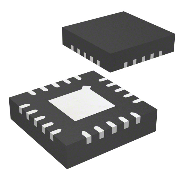
IS31FL3196A is available in QFN-20 (3mm × 3mm). It
operates from 2.7V to 5.5V over the temperature range
of -40°C to +85°C.
2.7V to 5.5V supply voltage
I2C interface
Rising edge of SDB reset I2C module
Two groups RGB, single color LED breathing
system-free pre-established pattern
6 independently controlled automatic and
semiautomatic breathing system-free
pre-established pattern
6 independently controlled outputs of 256 PWM
steps
8 levels programmable output current
Audio mode with AGC function
Cascade for the synchronization of chips
Over-temperature protection
QFN-20 (3mm × 3mm) package
APPLICATIONS
Mobile phones and other hand-held devices for
LED display
LED in home appliances
TYPICAL APPLICATION CIRCUIT
Figure 1
Typical Application Circuit
Note 1: The IC should be placed far away from the mobile antenna in order to prevent the EMI.
Lumissil Microsystems – www.lumissil.com
Rev. E, 08/20/2020
1
�IS31FL3196A
Figure 2
Lumissil Microsystems – www.lumissil.com
Rev. E, 08/20/2020
Typical Application Circuit (Cascade Mode)
2
�IS31FL3196A
PIN CONFIGURATION
Package
Pin Configuration (Top View)
QFN-20
PIN DESCRIPTION
No.
Pin
Description
1
VCC
Power supply.
2
C_FILT
Filter capacitor for audio control.
3~6
OUT1~OUT4
Current source outputs.
7
GND
Ground.
8, 9
OUT5~OUT6
Current source outputs.
10~12
NC
No connection.
13
SDB
Shutdown the chip when pulled to low.
14
I_AUD
Audio current input or output for cascade.
15
R_EXT
Input terminal used to connect an external resistor. The
value must be about 100kΩ.
16
AD
I2C address setting.
17
IN
Audio input.
18
SCL
I2C serial clock.
19
SDA
I2C serial data.
20
CLK/V_BM
CLK input or output for cascade.
When breathing mark function enable, this pin is V_BM
pin.
Thermal Pad
Need to connect to GND.
Lumissil Microsystems – www.lumissil.com
Rev. E, 08/20/2020
3
�IS31FL3196A
ORDERING INFORMATION
Industrial Range: -40°C to +85°C
Order Part No.
Package
QTY/Reel
IS31FL3196A-QFLS2-TR
QFN-20, Lead-free
2500
Copyright © 2020 Lumissil Microsystems. All rights reserved. Lumissil Microsystems reserves the right to make changes to this specification and its
products at any time without notice. Lumissil Microsystems assumes no liability arising out of the application or use of any information, products or
services described herein. Customers are advised to obtain the latest version of this device specification before relying on any published information and
before placing orders for products.
Lumissil Microsystems does not recommend the use of any of its products in life support applications where the failure or malfunction of the product can
reasonably be expected to cause failure of the life support system or to significantly affect its safety or effectiveness. Products are not authorized for use in
such applications unless Lumissil Microsystems receives written assurance to its satisfaction, that:
a.) the risk of injury or damage has been minimized;
b.) the user assume all such risks; and
c.) potential liability of Lumissil Microsystems is adequately protected under the circumstances
Lumissil Microsystems – www.lumissil.com
Rev. E, 08/20/2020
4
�IS31FL3196A
ABSOLUTE MAXIMUM RATINGS
Supply voltage, VCC
Voltage at any OUTx pins
Voltage at any input pins
GND terminal current
Maximum junction temperature, TJMAX
Storage temperature range, TSTG
Operating temperature range, TA=TJ
Package thermal resistance, junction to ambient (4 layer standard test
PCB based on JEDEC standard), θJA
ESD (HBM)
ESD (CDM)
-0.3V ~ +6.0V
-0.3V ~ +6.0V
-0.3V ~ VCC+0.3V
400mA
+150°C
-65°C ~ +150°C
-40°C ~ +85°C
58.1°C/W
±2kV
±1kV
Note 2: Stresses beyond those listed under “Absolute Maximum Ratings” may cause permanent damage to the device. These are stress
ratings only and functional operation of the device at these or any other condition beyond those indicated in the operational sections of the
specifications is not implied. Exposure to absolute maximum rating conditions for extended periods may affect device reliability.
ELECTRICAL CHARACTERISTICS
TA = 25°C, VCC = 2.7V ~ 5.5V, unless otherwise noted. Typical value are TA = 25°C, VCC = 5V.
Symbol
Parameter
VCC
Supply voltage
ICC
Quiescent power supply current
ISD
Shutdown current
IOUT
Output current
VHR
Current sink headroom voltage
Condition
Min.
Typ.
2.7
VSDB = VCC
3
VSDB = 0V
1
VSDB = VCC, software shutdown
2
PWM Control Mode, VDS = 0.4V
PWM Register(07h~0Ch) = 0xFF
20
(Note 3)
Audio Mode, Gain = 12dB
VIN = 0.8VP-P, 1kHz square wave
18
(Note 3)
IOUT = 20mA
Max.
Unit
5.5
V
mA
μA
mA
400
mV
Logic Electrical Characteristics (SDA, SCL, SDB, AD)
VIL
Logic “0” input voltage
VCC= 2.7V~5.5V
VIH
Logic “1” input voltage
VCC= 2.7V~5.5V
IIL
Logic “0” input current
SSD= “0”, VINPUT= 0V
5
(Note 4)
nA
IIH
Logic “1” input current
SSD= “0”, VINPUT= VCC
5
(Note 4)
nA
Lumissil Microsystems – www.lumissil.com
Rev. E, 08/20/2020
0.4
1.4
V
V
5
�IS31FL3196A
DIGITAL INPUT SWITCHING CHARACTERISTICS (Note 5)
Symbol
Parameter
Condition
Standard Mode
Min.
Typ.
Fast Mode
Max. Min.
Typ.
100
Max.
fSCL
Serial-Clock frequency
tBUF
Bus free time between a STOP and
a START condition
4.7
1.3
μs
tHD, STA
Hold time (repeated) START
condition
4.0
0.6
μs
tSU, STA
Repeated START condition setup
time
4.7
0.6
μs
tSU, STO
STOP condition setup time
4.0
0.6
μs
tHD, DAT
Data hold time (Note 6)
0
tSU, DAT
Data setup time (Note 7)
250
100
ns
tLOW
SCL clock low period
4.7
1.3
μs
tHIGH
SCL clock high period
4.0
0.7
μs
3.45
400
Unit
0
0.9
kHz
μs
tR
Rise time of both SDA and SCL
signals, receiving (Note 8)
1000
20+0.1Cb
300
ns
tF
Fall time of both SDA and SCL
signals, receiving (Note 8)
300
20+0.1Cb
300
ns
Note 3: The average current of each channel is IOUT.
Note 4: All LEDs are on.
Note 5: Guaranteed by design.
Note 6: The minimum tHD, DAT measured start from VIL(max) of SCL signal. The maximum tHD,DAT has only to be met if the device does not stretch
the LOW period (tLOW) of the SCL signal. VIL(max)
Note 7: A Fast-mode I2C-bus device can be used in a Standard-mode I2C-bus system, but the requirement tSU,DAT≥ 250 ns must then be met.
This will automatically be the case if the device does not stretch the LOW period of the SCL signal. If such a device does stretch the LOW period
of the SCL signal, it must output the next data bit to the SDA line tR max + tSU,DAT = 1000 + 250 = 1250ns (according to the Standard-mode I2C-bus
specification) before the SCL line is released.
Note 8: Cb= total capacitance of one bus line in pF. ISINK ≤ 6mA. tR and tF measured between 0.3 × VCC and 0.7 × VCC.
Lumissil Microsystems – www.lumissil.com
Rev. E, 08/20/2020
6
�IS31FL3196A
DETAILED DESCRIPTION
I2C INTERFACE
The IS31FL3196A uses a serial bus, which conforms to
the I2C protocol, to control the chip’s functions with two
wires: SCL and SDA. The IS31FL3196A has a 7-bit
slave address (A7:A1), followed by the R/W bit, A0.
Since IS31FL3196A only supports write operations, A0
must always be “0”. The value of bits A1 and A2 are
decided by the connection of the AD pin.
The complete slave address is:
Table 1 Slave Address (Write Only):
Bit
A7:A3
A2:A1
A0
Value
11001
AD
0
AD connected to GND, AD = 00;
AD connected to VCC, AD = 11;
AD connected to SCL, AD = 01;
AD connected to SDA, AD = 10;
The SCL line is uni-directional. The SDA line is
bi-directional (open-collector) with a pull-up resistor
(typically 4.7kΩ). The maximum clock frequency
specified by the I2C standard is 400kHz. In this
discussion, the master is the microcontroller and the
slave is the IS31FL3196A.
The timing diagram for the I2C is shown in Figure 3.
The SDA is latched in on the stable high level of the
SCL. When there is no interface activity, the SDA line
should be held high.
Figure 3
Figure 4
Lumissil Microsystems – www.lumissil.com
Rev. E, 08/20/2020
The “START” signal is generated by lowering the SDA
signal while the SCL signal is high. The start signal will
alert all devices attached to the I2C bus to check the
incoming address against their own chip address.
The 8-bit chip address is sent next, most significant bit
first. Each address bit must be stable while the SCL
level is high.
After the last bit of the chip address is sent, the master
checks for the IS31FL3196A’s acknowledge. The
master releases the SDA line high (through a pull-up
resistor). Then the master sends an SCL pulse. If the
IS31FL3196A has received the address correctly, then
it holds the SDA line low during the SCL pulse. If the
SDA line is not low, then the master should send a
“STOP” signal (discussed later) and abort the transfer.
Following acknowledge of IS31FL3196A, the register
address byte is sent, most significant bit first.
IS31FL3196A must generate another acknowledge
indicating that the register address has been received.
Then 8-bit of data byte are sent next, most significant
bit first. Each data bit should be valid while the SCL
level is stable high. After the data byte is sent, the
IS31FL3196A must generate another acknowledge to
indicate that the data was received.
The “STOP” signal ends the transfer. To signal “STOP”,
the SDA signal goes high while the SCL signal is high.
Interface Timing
Bit Transfer
7
�IS31FL3196A
Figure 5
Writing to IS31FL3196A
REGISTERS DEFINITIONS
Table 2 Register Function
Address
Name
Function
R/W
Table
Default
00h
Shutdown Register
Set software shutdown mode
3
0000 0000
01h
LED Control Register
OUT1~ OUT6 enable bit
4
0111 0111
03h
Configuration Register 1
Set operation mode
5
04h
Configuration Register 2
Set output current and audio input gain
6
05h
Ramping Mode Register
Set the ramping function mode
7
06h
Breathing Mark Register
Set the breathing mark function
8
PWM Register
6 channels PWM duty cycle data registers
Data Update Register
Load PWM Registers and LED Control
Registers’ data
11h ~ 16h
T0 Register
Set the T0 time
10
1Ah ~ 1Bh
T1~T3 Register
Set the T1~T3 time
11
1Dh ~ 22h
T4 Register
Set the T4 time
12
26h
Time Update Register
Load time registers’ data
-
FFh
Reset Register
Reset all registers to default value
-
07h ~ 0Ch
10h
0000 0000
9
W
-
xxxx xxxx
0000 0000
xxxx xxxx
Table 4 01h LED Control Register (OUT1~OUT6)
Table 3 00h Shutdown Register
Bit
D7:D1
D0
Bit
D7
D6:D4
D3
D2:D0
Name
-
SSD
Name
-
OUT6:OUT4
-
OUT3:OUT1
Default
0000000
0
Default
0
111
0
111
The Shutdown Register sets software shutdown mode
of IS31FL3196A.
SSD
0
1
Software Shutdown Enable
Software shutdown mode
Normal operation
Lumissil Microsystems – www.lumissil.com
Rev. E, 08/20/2020
The LED Control Registers store the on or off state of
each channel LED.
OUTx
0
1
LED State
LED off
LED on
8
�IS31FL3196A
Table 5 03h Configuration Register 1
Bit
D7:D6
D5:D4
D3
Name
-
RGB2:1
-
Default
00
00
0
D2
D1
D0
AE AGCE AGCM
0
0
0
The Configuration Register 1 sets operation mode.
RGBx
0
1
RGB Mode Selection
PWM Control Mode
One Shot Programming Mode
AE
0
1
Audio Modulate Enable
Disable
Enable
AGCE
0
1
AGC Function Enable
Enable
Disable
AGCM
0
1
AGC Mode Selection
Mode1 (Fast Modulation)
Mode2 (Slow Modulation)
AGS
000
001
010
011
100
101
110
111
Audio Gain Selection
Gain= 0dB
Gain= 3dB
Gain= 6dB
Gain= 9dB
Gain= 12dB
Gain= 15dB
Gain= 18dB
Gain= 21dB
Table 7 05h Ramping Mode Register
Bit
D7:D6
D5:D4
D3:D2
D1:D0
Name
-
RM(RGB2:1)
-
HT(RGB2:1)
Default
00
00
00
00
The Ramping Mode Register sets the ramping
function.
Table 6 04h Configuration Register 2
RM
0
1
Ramping Mode Enable
Disable
Enable
HT
0
1
Hold Time Selection
Breathing Hold on T2
Breathing Hold on T4
Bit
D7
D6:D4
D3
D2:D0
Name
CM
CS
-
AGS
Bit
D7:D5
D4
D3
D2:D0
Default
0
000
0
000
Name
-
BME
-
CSS
Default
000
0
0
000
The Configuration Register 2 stores the intensity control
settings for all of the LEDs and the control mode.
CM
0
1
Control Mode
Master
Slave
CS
000
001
010
011
100
101
110
111
Current Setting
20mA
15mA
10mA
5mA
40mA
35mA
30mA
25mA
Lumissil Microsystems – www.lumissil.com
Rev. E, 08/20/2020
Table 8 06h Breathing Mark Register
The Breathing Mark Register sets the breathing mark
function (Detail information refers to Page 12).
BME
0
1
Breathing Mark Enable
Disable
Enable
CSS
000
001
010
011
100
101
Others
Channel Selection
OUT1
OUT2
OUT3
OUT4
OUT5
OUT6
Unavailable
9
�IS31FL3196A
Table 9 07h~0Ch PWM Register (OUT1~OUT6)
Bit
D7:D0
Name
PWM
Default
0000 0000
The PWM Registers can modulate RGB light with 256
different items.
The value of PWM Registers decide the average output
current of OUT1~OUT6. The average output current
may be computed using the Formula (1):
I OUT
I MAX 7
D[ n] 2 n
256 n 0
(1)
Where “n” indicates the bit location in the respective
PWM register.
For example: D7:D0 = 10110101,
IOUT = IMAX (20+22+24+25+27)/256
IMAX is set by Configuration Register2 (04h).
10h Data Update Register
The data sent to the PWM Registers and the LED
Control Registers will be stored in temporary registers.
A write operation of “0000 0000” value to the Data
Update Register is required to update the registers
(01h, 07h~0Ch).
Table 10 11h~16h T0 Register (OUT1~OUT6)
Bit
D7:D6
D5:D4
D3:D0
Name
-
B
A
Default
00
00
0000
The T0 Registers set the T0 time in One Shot
Programming Mode.
T0 = τ×A×2B
A = 0~15, B = 0~3 and τ = 260ms (Typ.)
For example, the max T0 is 260ms×15×23 = 31.2s
Double Time
T3 =T1
T3 = 2T1
DT
0
1
If A = 0~4, T1 = T3 = τ×2A, τ = 260ms (Typ.)
If A = 5~6, the breathing function disable.
If A = 7, T1= T3 = 0.1ms.
If B = 1~7, T2 = τ×2B-1, τ = 260ms (Typ.)
If B = 0, T2 = 0s.
For example, the max T1&T3 is 260ms×24 = 4.16s.
The max T2 is 260ms×26 = 16.64s.
Table 12 1Dh~22h T4 Register (OUT1~OUT6)
Bit
D7:D6
D5:D4
D3:D0
Name
-
B
A
Default
00
00
0000
The T4 Registers set the T4 time in One Shot
Programming Mode.
T4 = τ×A×2B
A = 0~15, B = 0~3 and τ = 260ms (Typ.)
For example, the max T4 is 260ms×15×23 = 31.2s
26h Time Update Register
The data sent to the time registers (11h~16h,
1Ah~1Bh, 1Dh~22h) will be stored in temporary
registers. A write operation of “0000 0000” data to the
Time Update Register is required to update the
registers (11h~16h, 1Ah~1Bh, 1Dh~22h).
FFh Reset Register
Once user writes “0000 0000” data to the Reset
Register, IS31FL3196A will reset all registers to default
value. On initial power-up, the IS31FL3196A registers
are reset to their default values for a blank display.
Table 11 1Ah~1Bh T1~T3 Register (RGB1~RGB2)
Bit
D7
D6:D4
D3
D2:D0
Name
DT
B
-
A
Default
0
000
0
000
The T1~T3 Registers set the T1~T3 time in One Shot
Programming Mode.
Lumissil Microsystems – www.lumissil.com
Rev. E, 08/20/2020
10
�IS31FL3196A
FUNCTIONAL BLOCK DIAGRAM
Lumissil Microsystems – www.lumissil.com
Rev. E, 08/20/2020
11
�IS31FL3196A
APPLICATION INFORMATION
GENERAL DESCRIPTION
IS31FL3196A is a 6-channel LED driver with
two-dimensional auto breathing and PWM Control
mode. It can drive six LEDs or two groups RGB.
POWER ON SEQUENCE
IS31FL3196A provides a power-on reset feature that is
controlled by VBAT (voltage at pin1) supply voltage.
When the VBAT exceeds 2.0V (POR_H, Typ.), the
internal circuit starts to work. The reset signal will be
generated to perform a power-on reset (POR_H)
operation, which will reset all control circuits and
configuration registers until the internal power voltage
become stable.
Before SDB pull high, the I2C operation is allowed. The
SDB rising edge will reset the I2C bus.
RGB BREATHING CONTROL WITH AUTO COLOR
CHANGING
By setting the RGBx bits of the Configuration Register
1 (03h) to “1”, the IS31FL3196A will operate in One
Shot Programming mode. In this mode each group
RGB can be modulated breathing cycle independently
by T0~T4. The full cycle is T1 to T4 (Figure 8). Setting
different T0~T4 can achieve RGB breathing with auto
color changing. The maximum intensity of each RGB
can be adjusted independently by the PWM Registers
(07h~0Ch).
Note, if IS31FL3196A operates in the One Shot
Programming mode and then enters into the shutdown
mode, an 8-bit data write operation to the Time Update
Register is required to restart the LED breathing effect
after the IC is re-enabled.
Figure 8
Breathing Timing
RGB AUTO BREATHING CONTROL WITH COLOR
SETTING
Figure 7 SDB Pin Sequence
Note 1: I2C operation is allowed when SDB is low.
Note 2: There should be no I2C operation 10µs before and after SDB
rinsing edge.
In some case, like a mouse, when plug-out and quickly
plug-in back the USB power, the LED will flash for a
very short time. The reason is the power is not lower
than the POR_L voltage point 1.92V (Typ.), and the
device still stores the previous setting data, if user
pull-up the SDB high when power up, following with the
initial operation, the LED will be ON between SDB rising
edge and PWM initial effective, to avoid this, as above
figure, a writing to 00h is recommended to shutdown
the chip before pull-high the SDB pin.
PWM CONTROL
By setting the RGBx bits of the Configuration Register
1 (03h) to “0”, the IS31FL3196A will operate in PWM
Control mode. The PWM Registers (07h~0Ch) can
modulate LED brightness of 6 channels with 256 steps.
For example, if the data in PWM Register is “0000
0100”, then the PWM is the fourth step.
Writing new data continuously to the registers can
modulate the brightness of the LEDs to achieve a
breathing effect.
Lumissil Microsystems – www.lumissil.com
Rev. E, 08/20/2020
IS31FL3196A can pre-establish pattern achieving
mixing color breathing. There are two groups RGB.
Each RGB consists of three channels. Every channel
has an 8-bit PWM data register. The color can be set
by the PWM data register. For example, there are three
PWM data: 20h, 80h, C8h, so the three data will
determine a kind of color.
After setting the color, T0~T4 time register will be set to
control the LED breathing panel. And T0~T4 time
should be same for one RGB or the pre-established
color will change.
SEMIAUTOMATIC BREATHING
By setting the RGBx bits of the Configuration Register
1 (03h) to “1” and the RM bit of the Ramping Mode
Register (05h) to “1”, the ramping function is enabled.
HT is the time select bit. When HT bit is set to “0”, T2
will be held forever, and the LED will remain at the
programmed maximum intensity. When HT bit is set to
“1”, T3 will continue and T4 will be held, causing the
LED to complete one breathing cycle and then remain
off.
AUDIO MODULATE DISPLAY MODE WITH AGC
FUNCTION
In audio modulate display mode the output current can
be modulated by the audio input signal. An AGC
automatically adjusts the audio input gain to improve
the dynamic range of the LED current modulation, thus
improving the visual effect. When the input signal is
12
�IS31FL3196A
large such that the amplifier output begins to clip, the
gain goes down. If the input signal is small, the gain
increases, adjusting the output to provide a good
dynamic response to the input signal.
The AGC can be disabled and the audio gain can be
set by programming Configuration Register 1 (03h).
BREATHING MARK FUNCTION
By setting the BME bit of the Breathing Mark Register
(06h) to “1”, the breathing mark function is enabled.
The CLK/V_BM pin is used as V_BM. If the BME bit
sets to “0”, the breathing mark function disabled. The
CLK/V_BM pin is used as CLK, V_BM is an output pin.
The breathing mark function is useful as a signal to
notify the MCU when to update the color data. At the
end of time period T1, V_BM will induce a falling edge
and hold logic low, so the new data can be sent by MCU
at this time. At the end of T3, V_BM will induce a rising
edge and the MCU can send an update command to
update all data simultaneously (Figure 8). The marking
channel (OUT1~OUT6) is selected by the CSS bits of
the Breathing Mark Register (06h).
When IS31FL3196A operates as slave, the breathing
mark function is unavailable.
Notice the CLK/V_BM output is push-pull structure and
high logic is VCC (same as Pin 1), so when this pin is
connected to controller GPIO, a 10kΩ resistor is
recommended, otherwise the output pin voltage will
higher than the GPIO pin.
T0
T1
T2
T3
T4
CASCADE FOR SYNCHRONIZATION OF CHIPS
Operating in the cascade mode can make two chips
synchronize (Figure 2). By setting the CM bit of
Configuration Register 2 (04h) to “0”, IS31FL3196A
operates as a master. There are two pins (CLK, I_AUD)
for synchronization of chips. CLK pin can synchronize
the breathing and I_AUD pin can synchronize the
audio current.
SHUTDOWN MODE
Shutdown mode can either be used as a means of
reducing power consumption or generating a flashing
display (repeatedly entering and leaving shutdown
mode). During shutdown mode all registers retain their
data.
Software Shutdown
By setting SSD bit of the Shutdown Register (00h) to
“0”, the IS31FL3196A will operate in software
shutdown mode, wherein they consume only 2μA (typ.)
current. When the IS31FL3196A is in software
shutdown mode, all current sources are switched off.
Hardware Shutdown
The chip enters hardware shutdown mode when the
SDB pin is pulled low, wherein they consume only 1μA
(Typ.) current. When set SDB high, the rising edge will
reset the I2C module, but the register information
retains.
T1
Full Cycle
V_BM
Figure 9
V_BM Signal
Lumissil Microsystems – www.lumissil.com
Rev. E, 08/20/2020
13
�IS31FL3196A
CLASSIFICATION REFLOW PROFILES
Profile Feature
Pb-Free Assembly
Preheat & Soak
Temperature min (Tsmin)
Temperature max (Tsmax)
Time (Tsmin to Tsmax) (ts)
150°C
200°C
60-120 seconds
Average ramp-up rate (Tsmax to Tp)
3°C/second max.
Liquidous temperature (TL)
Time at liquidous (tL)
217°C
60-150 seconds
Peak package body temperature (Tp)*
Max 260°C
Time (tp)** within 5°C of the specified
classification temperature (Tc)
Max 30 seconds
Average ramp-down rate (Tp to Tsmax)
6°C/second max.
Time 25°C to peak temperature
8 minutes max.
Figure 10
Classification Profile
Lumissil Microsystems – www.lumissil.com
Rev. E, 08/20/2020
14
�IS31FL3196A
PACKAGE INFORMATION
QFN-20
Lumissil Microsystems – www.lumissil.com
Rev. E, 08/20/2020
15
�IS31FL3196A
RECOMMENDED LAND PATTERN
QFN-20
Note:
1. Land pattern complies to IPC-7351.
2. All dimensions in MM.
3. This document (including dimensions, notes & specs) is a recommendation based on typical circuit board manufacturing parameters. Since
land pattern design depends on many factors unknown (eg. user’s board manufacturing specs), user must determine suitability for use.
Lumissil Microsystems – www.lumissil.com
Rev. E, 08/20/2020
16
�IS31FL3196A
REVISION HISTORY
Revision
Detail Information
Date
0A
Initial release
2016.08.09
A
Update POD, release to mass production
2016.08.29
B
1. Correct nine channels to six
2. Update θJA
2017.03.21
C
Update land pattern
2017.11.01
D
1. VIH, VIL condition revise to VCC= 2.7V~5.5V
2. Add STANDARD MODE in DIGITAL INPUT SWITCHING CHARACTERISTICS
3. Update θJA value
4. Update IIH/IIL test condition
5. Add POWER ON SEQUENCE section in APPLICATION INFORMATION
2018.04.27
E
Update POD and land pattern
2020.08.20
Lumissil Microsystems – www.lumissil.com
Rev. E, 08/20/2020
17
�


 工商网监
湘ICP备2023018690号
工商网监
湘ICP备2023018690号
