Uniform Sector
Standard and Quad Serial Flash
GD25LT256E
DATASHEET
1
GD25LT256E
�Uniform Sector
Standard and Quad Serial Flash
GD25LT256E
Contents
1
FEATURES .........................................................................................................................................................5
2
GENERAL DESCRIPTIONS..............................................................................................................................6
3
MEMORY ORGANIZATION ............................................................................................................................. 10
4
DEVICE OPERATIONS.................................................................................................................................... 11
4.1
SPI MODE ............................................................................................................................................................ 11
4.2
QPI MODE............................................................................................................................................................ 11
4.3
QUAD DTR MODE ................................................................................................................................................. 11
4.4
RESET FUNCTION .................................................................................................................................................. 11
4.5
ECC FUNCTION ...................................................................................................................................................... 12
4.6
DATA STROBE FUNCTION ......................................................................................................................................... 12
5
DATA PROTECTION ........................................................................................................................................ 13
6
DATA INTEGRITY CHECK .............................................................................................................................. 15
7
8
9
6.1
ECC (ERROR CHECKING AND CORRECTING) ................................................................................................................. 15
6.2
ECS# (ERROR CORRECTED SIGNAL) PIN ...................................................................................................................... 16
6.3
PARITY CHECK (CRC) .............................................................................................................................................. 16
REGISTERS...................................................................................................................................................... 17
7.1
STATUS REGISTER ................................................................................................................................................... 17
7.2
FLAG STATUS REGISTER ........................................................................................................................................... 18
7.3
EXTENDED ADDRESS REGISTER .................................................................................................................................. 19
INTERNAL CONFIGURATION REGISTER ................................................................................................... 21
8.1
NONVOLATILE CONFIGURATION REGISTER ................................................................................................................... 21
8.2
VOLATILE CONFIGURATION REGISTER ......................................................................................................................... 23
8.3
SUPPORTED CLOCK FREQUENCIES .............................................................................................................................. 26
8.4
DATA SEQUENCE WRAPS BY DENSITY ......................................................................................................................... 27
COMMAND DESCRIPTIONS .......................................................................................................................... 28
9.1
ENABLE 4-BYTE MODE (B7H) .................................................................................................................................. 33
9.2
DISABLE 4-BYTE MODE (E9H) .................................................................................................................................. 33
9.3
WRITE ENABLE (WREN) (06H) ................................................................................................................................ 34
9.4
WRITE DISABLE (WRDI) (04H) ................................................................................................................................ 34
9.5
WRITE ENABLE FOR VOLATILE STATUS REGISTER (50H) ................................................................................................. 35
9.6
WRITE STATUS REGISTER (WRSR) (01H) ................................................................................................................... 35
9.7
WRITE EXTENDED ADDRESS REGISTER (C5H)............................................................................................................... 36
9.8
WRITE NONVOLATILE/VOLATILE CONFIGURATION REGISTER (B1H/81H) ......................................................................... 37
9.9
READ STATUS REGISTER (05H) ................................................................................................................................. 38
2
�Uniform Sector
Standard and Quad Serial Flash
GD25LT256E
9.10
READ FLAG STATUS REGISTER (70H) .......................................................................................................................... 39
9.11
READ NONVOLATILE/VOLATILE CONFIGURATION REGISTER (B5H/85H) ........................................................................... 40
9.12
READ EXTENDED ADDRESS REGISTER (C8H) ................................................................................................................ 41
9.13
READ DATA BYTES (03H/13H) ................................................................................................................................ 42
9.14
READ DATA BYTES AT HIGHER SPEED (0BH/0CH) ........................................................................................................ 43
9.15
QUAD OUTPUT FAST READ (6BH/6CH) ..................................................................................................................... 44
9.16
QUAD I/O FAST READ (EBH/ECH) ........................................................................................................................... 45
9.17
QUAD I/O DTR READ (EDH/EEH) ........................................................................................................................... 47
9.18
PAGE PROGRAM (PP) (02H/12H) ............................................................................................................................ 49
9.19
QUAD PAGE PROGRAM (32H/34H) .......................................................................................................................... 50
9.20
EXTEND QUAD PAGE PROGRAM (C2H/3EH) .............................................................................................................. 52
9.21
SECTOR ERASE (SE) (20H/21H) ............................................................................................................................... 53
9.22
32KB BLOCK ERASE (BE32) (52H/5CH) ................................................................................................................... 54
9.23
64KB BLOCK ERASE (BE64) (D8H/DCH) .................................................................................................................. 55
9.24
CHIP ERASE (CE) (60/C7H) ..................................................................................................................................... 56
9.25
ENABLE QPI (38H) ................................................................................................................................................ 57
9.26
DISABLE QPI (FFH) ................................................................................................................................................ 57
9.27
DEEP POWER-DOWN (DP) (B9H) ............................................................................................................................. 57
9.28
RELEASE FROM DEEP POWER-DOWN (ABH) ............................................................................................................... 58
9.29
READ UNIQUE ID (4BH) .......................................................................................................................................... 59
9.30
READ IDENTIFICATION (RDID) (9FH/9EH) ................................................................................................................. 60
9.31
PROGRAM/ERASE SUSPEND (PES) (75H) ................................................................................................................... 61
9.32
PROGRAM/ERASE RESUME (PER) (7AH) ................................................................................................................... 62
9.33
ERASE SECURITY REGISTERS (44H) ............................................................................................................................ 63
9.34
PROGRAM SECURITY REGISTERS (42H) ....................................................................................................................... 64
9.35
READ SECURITY REGISTERS (48H) ............................................................................................................................. 65
9.36
INDIVIDUAL BLOCK/SECTOR LOCK (36H)/UNLOCK (39H)/READ (3DH) ........................................................................... 66
9.37
GLOBAL BLOCK/SECTOR LOCK (7EH) OR UNLOCK (98H) ............................................................................................... 69
9.38
ENABLE RESET (66H) AND RESET (99H) ..................................................................................................................... 69
9.39
READ SERIAL FLASH DISCOVERABLE PARAMETER (5AH)................................................................................................. 70
10
ELECTRICAL CHARACTERISTICS .......................................................................................................... 72
10.1
POWER-ON TIMING ................................................................................................................................................ 72
10.2
INITIAL DELIVERY STATE ........................................................................................................................................... 72
10.3
ABSOLUTE MAXIMUM RATINGS ................................................................................................................................ 72
10.4
CAPACITANCE MEASUREMENT CONDITIONS................................................................................................................. 73
10.5
DC CHARACTERISTICS .............................................................................................................................................. 74
10.6
AC CHARACTERISTICS .............................................................................................................................................. 77
11
ORDERING INFORMATION........................................................................................................................ 86
11.1
12
12.1
VALID PART NUMBERS ............................................................................................................................................ 87
PACKAGE INFORMATION ......................................................................................................................... 88
PACKAGE SOP16 300MIL ...................................................................................................................................... 88
3
�Uniform Sector
Standard and Quad Serial Flash
GD25LT256E
12.2
PACKAGE WSON8 (8X6MM) ................................................................................................................................... 89
12.3
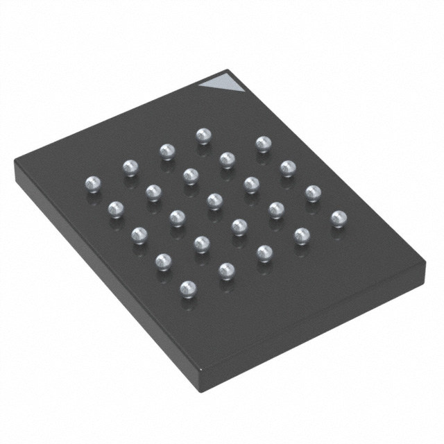
PACKAGE TFBGA-24BALL (5X5 BALL ARRAY) ............................................................................................................. 90
13
REVISION HISTORY .................................................................................................................................... 91
4
�Uniform Sector
Standard and Quad Serial Flash
GD25LT256E
1 FEATURES
◆ 256M-bit Serial Flash
◆ Fast Program/Erase Speed
- 32M-Byte
- Page Program time: 0.3ms typical
- 256 Bytes per programmable page
- Sector Erase time: 30ms typical
- Block Erase time: 0.1/0.2s typical
◆ Standard, Quad SPI, DTR,QPI
- Chip Erase time: 50s typical
- Standard SPI: SCLK, CS#, SI, SO, WP#, RESET#
- Quad SPI: SCLK, CS#, IO0, IO1, IO2, IO3, RESET#
◆ Flexible Architecture
- QPI: SCLK, CS#, IO0, IO1, IO2, IO3, RESET#
- Sector of 4K-Byte
- SPI DTR (Double Transfer Rate) Read
- Block of 32/64K-Byte
- 3 or 4-Byte Address Mode
- Erase/Program Suspend/Resume
◆ High Speed Clock Frequency
◆ Low Power Consumption
- 200MHz for fast read
- 20μA typical stand-by current
- Quad I/O Data transfer up to 664Mbits/s
- 5μA typical power-down current
- QPI Mode Data transfer up to 664Mbits/s
- DTR Quad I/O Data transfer up to 200MBytes/s with DQS
◆ Advanced Security Features
- 128-bit Unique ID
◆ Allows XIP (eXecute in Place) Operation
- 4K-Byte Security Registers With OTP Lock
- High speed Read reduce overall XiP instruction fetch time
- Continuous Read with Wrap further reduce data latency to
fill up SoC cache
◆ Single Power Supply Voltage
- Full voltage range: 1.65~2.0V
◆ Software/Hardware Write Protection
◆ Endurance and Data Retention
- Write protect all/portion of memory via software
- Minimum 100,000 Program/Erase Cycles
- Enable/Disable protection with WP# Pin
- 20-year data retention typical
- Individual Block Protection
◆ Package Information
◆ Data Integrity Check
- On-chip ECC (1-bit correction every
- SOP16 300mil
8-Byte) (1)
- WSON8 (8x6mm)
- CRC detects accidental changes to raw data
- TFBGA-24ball (5x5 Ball Array)
Note:
1. When ECC is enabled, it is required to program minimum one or multiple aligned 8-Byte granularities. Every aligned 8Byte granularity should only be programmed once before Erase to ensure correct ECC operations.
5
�Uniform Sector
Standard and Quad Serial Flash
2
GD25LT256E
GENERAL DESCRIPTIONS
The GD25LT256E (256M-bit) Serial flash supports the standard Serial Peripheral Interface (SPI), and supports the Quad
SPI and DTR mode: Serial Clock, Chip Select, Serial Data I/O0 (SI), I/O1 (SO), I/O2 (WP#), I/O3,DQS, ECS# and
RESET#. The Quad I/O & Quad output data is transferred with speed of 83MBytes/s, and the DTR Quad I/O data is
transferred with speed of 200MBytes/s.
CONNECTION DIAGRAM AND PIN DESCRIPTION
Figure 1 Connection Diagram for SOP16 package
IO3
1
16
SCLK
VCC
2
15
SI
(IO0)
RESET#
3
14
NC
NC
4
13
DQS
Top View
NC
5
12
NC
DNU
6
11
DNU
CS#
7
10
VSS
SO
(IO1)
8
9
WP#
(IO2)
16-LEAD SOP
Table 1 Pin Description for SOP16 package
Pin No.
Pin Name
I/O
Description
1
IO3
I/O
Data Input Output 3
2
VCC
3
RESET#
6/11
DNU
7
CS#
I
8
SO (IO1)
I/O
Data Output (Data Input Output 1)
9
WP# (IO2)
I/O
Data Input Output 2
10
VSS
13
DQS
O
Data Strobe Signal Output
15
SI (IO0)
I/O
Data Input (Data Input Output 0)
16
SCLK
I
Power Supply
I
Reset Input
Do Not Use (It may connect to internal signal inside)
Chip Select Input
Ground
Serial Clock Input
Note:
1. CS# must be driven high if chip is not selected. Please don’t leave CS# floating any time after power is on.
2. The DNU pin must be floating. It may connect to internal signal inside.
3. The NC pin is not connected to any internal signal. It is OK to connect it to the system ground (GND) or leave it floating.
6
�Uniform Sector
Standard and Quad Serial Flash
GD25LT256E
4. RESET# will remain internal pull up function while this pin is not physically connected in system configuration. However,
the internal pull up function will be disabled if the system has physical connection to RESET#.
Figure 2 Connection Diagram for WSON8 package
CS#
1
SO
(IO1)
2
WP#
(IO2)
3
6 SCLK
VSS
4
5
8
VCC
7
IO3
Top View
SI
(IO0)
8–LEAD WSON
Table 2 Pin Description for WSON8 package
Pin No.
Pin Name
I/O
Description
1
CS#
I
2
SO (IO1)
I/O
Data Output (Data Input Output 1)
3
WP# (IO2)
I/O
Write Protect Input (Data Input Output 2)
4
VSS
5
SI (IO0)
I/O
6
SCLK
I
7
IO3
I/O
8
VCC
Chip Select Input
Ground
Data Input (Data Input Output 0)
Serial Clock Input
Data Input Output 3
Power Supply
Note:
1.
CS# must be driven high if chip is not selected. Please don’t leave CS# floating any time after power is on.
7
�Uniform Sector
Standard and Quad Serial Flash
GD25LT256E
Figure 3 Connection Diagram for TFBGA24 5x5 ball array package
Top View
A2
A3
A4
A5
RESET# ECS#
NC
NC
B1
B2
B3
B4
B5
NC
SCLK
VSS
VCC
NC
C1
C2
C3
C4
C5
CS#
DQS
WP#
(IO2)
DNU
D2
D3
VSS
D1
VCC
SO(IO1) SI(IO0)
D4
D5
IO3
NC
E1
E2
E3
E4
E5
NC
NC
NC
VCC
VSS
24-BALL TFBGA (5x5 ball array)
Table 3 Ball Description for TFBGA24 5x5 ball array package
Pin No.
Pin Name
I/O
Description
A4
RESET#
I
Reset Input
A5
ECS#
O
ECC Correction Signal (Open Drain)
B2
SCLK
I
Serial Clock Input
B3/C1/E5
VSS
Ground
B4/D1/E4
VCC
Power Supply
C2
CS#
I
Chip Select Input
C3
DQS
O
Data Strobe Signal Output
C4
WP# (IO2)
I/O
Data Input Output 2
C5
DNU
D2
SO (IO1)
I/O
Data Output (Data Input Output 1)
D3
SI (IO0)
I/O
Data Input (Data Input Output 0)
D4
IO3
I/O
Data Input Output 3
Do Not Use (It may connect to internal signal inside)
Note:
1. CS# must be driven high if chip is not selected. Please don’t leave CS# floating any time after power is on.
2. The DNU ball must be floating. It may connect to internal signal inside.
3. The NC ball is not connected to any internal signal. It is OK to connect it to the system ground (GND) or leave it floating.
4. RESET# will remain internal pull up function while this pin is not physically connected in system configuration. However,
the internal pull up function will be disabled if the system has physical connection to RESET#.
8
�Uniform Sector
Standard and Quad Serial Flash
GD25LT256E
BLOCK DIAGRAM
Write Control
Logic
Status
Register
RESET#
IO2
IO3
SCLK
CS#
SI(IO0)
SPI
Command &
Control Logic
High Voltage
Generators
Page Address
Latch/Counter
Flash
Memory
Column Decode And
256-Byte Page Buffer
SO(IO1)
DQS
ECS#
Write Protect Logic
and Row Decode
WP#
Byte Address
Latch/Counter
9
�Uniform Sector
Standard and Quad Serial Flash
3
GD25LT256E
MEMORY ORGANIZATION
GD25LT256E
Each device has
Each block has
Each sector has
Each page has
32M
64/32K
4K
256
Bytes
128K
256/128
16
-
pages
8K
16/8
-
-
sectors
512/1K
-
-
-
blocks
UNIFORM BLOCK SECTOR ARCHITECTURE
GD25LT256E 64K Bytes Block Sector Architecture
Block
511
510
……
……
2
1
0
Sector
Address range
8191
1FFF000H
1FFFFFFH
……
……
……
8176
1FF0000H
1FF0FFFH
8175
1FEF000H
1FEFFFFH
……
……
……
8160
1FE0000H
1FE0FFFH
……
……
……
……
……
……
……
……
……
……
……
……
……
……
……
……
……
……
47
02F000H
02FFFFH
……
……
……
32
020000H
020FFFH
31
01F000H
01FFFFH
……
……
……
16
010000H
010FFFH
15
00F000H
00FFFFH
……
……
……
0
000000H
000FFFH
10
�Uniform Sector
Standard and Quad Serial Flash
GD25LT256E
4 DEVICE OPERATIONS
4.1
SPI Mode
Standard SPI
The GD25LT256E features a serial peripheral interface on 4 signals bus: Serial Clock (SCLK), Chip Select (CS#), Serial
Data Input (SI) and Serial Data Output (SO). Both SPI bus mode 0 and 3 are supported. Input data is latched on the rising
edge of SCLK and data shifts out on the falling edge of SCLK.
Quad SPI
The GD25LT256E supports Quad SPI operation when using the “Quad Output Fast Read”, “Quad I/O Fast Read”, “Quad
Page Program” (6BH/6CH, EBH/ECH, 32H/34H, C2H/3EH) commands. These commands allow data to be transferred
to or from the device at four times the rate of the standard SPI. When using the Quad SPI command the SI and SO pins
become bidirectional I/O pins: IO0 and IO1.
DTR Quad SPI
The GD25LT256E supports DTR Quad SPI operation when using the “DTR Quad I/O Fast Read” (EDH/EEH) command.
These commands allow data to be transferred to or from the device at eight times the rate of the standard SPI, and data
output will be latched on both rising and falling edges of the serial clock. When using the DTR Quad SPI command the
SI and SO pins become bidirectional I/O pins: IO0 and IO1.
4.2
QPI Mode
The GD25LT256E supports Quad Peripheral Interface (QPI) operations only when the device is switched from
Standard/Quad SPI mode to QPI mode using the “Enable the QPI (38H)” command. The QPI mode utilizes all four IO pins
to input the command code. Standard/Quad SPI mode and QPI mode are exclusive. Only one mode can be active at any
given times. “Enable the QPI (38H)” and “Disable the QPI (FFH)” commands are used to switch between these two modes.
Upon power-up and after software reset using “Enable Reset (66H) and Reset (99H)” command, the default state of the
device is Standard/Quad SPI mode.
4.3
Quad DTR Mode
The GD25LT256E supports Quad DTR operations only when the device is in Quad DTR mode, which could be entered by
setting Byte in Configuration Register as E7H/C7H with the “Write Volatile Configuration Register command (81H)”. The
Quad DTR Mode utilizes all four IO pins to input the command code latched on the rising edge of SCLK. All four IO pins are
used to input the address output the data on both rising and falling edges of SCLK.
4.4
RESET Function
The RESET# pin allows the device to be reset by the control.
The RESET# pin goes low for a minimum period of tRLRH will reset the flash. After reset cycle, the flash is at the following
states:
- Standby mode
- All the volatile bits will return to the default status as power on.
11
�Uniform Sector
Standard and Quad Serial Flash
GD25LT256E
Figure 4 RESET Condition
CS#
RESET#
RESET
4.5
ECC Function
The ECC Correction Signal (ECS#) pin is provided to the system hardware designers to determine the ECC status during
any Read operation. The ECS# pin will be pulled low during any 8-Byte Read data output period in which an ECC event
has occurred. ECS# pin can be used to represent SEC (Single Error Correction) event. ECC Correction Signal Output
pin is an Open-Drain connection.
4.6
Data Strobe Function
The Data Strobe function is enabled as default for this device, and the DQS pin is an active output pin for the Data Strobe
(DQS) signal during Read operations. The DQS signal is typically used in high speed applications to indicate when the
output data is ready to be fetched by the controllers. When the data strobe function is enabled, DQS signal is driven to
ground once CS# goes LOW, and will start to toggle when the output data is ready on the I/O pins. The toggling frequency
is the same as the CLK frequency. For STR Read operations, the data should only be latched on the rising edge of DQS
signal. For DTR Read operations, the data should be latched on both rising edge and falling edge of the DQS signal.
The Data Strobe function can also be disabled by setting the non-volatile or volatile Configuration Register Byte.
Please refer to the Configuration Register description for details. When disabled, the DQS signal is not driven and will
stay at Hi-Z state.
12
�Uniform Sector
Standard and Quad Serial Flash
5
GD25LT256E
DATA PROTECTION
The GD25LT256E provide the following data protection methods:
◆
Write Enable (WREN) command: The WREN command is set the Write Enable Latch bit (WEL). The WEL bit will
return to reset by the following situation:
- Power-Up/ Software reset (66H+99H)
- Write Disable (WRDI)
- Write Status Register (WRSR)
- Write Extended Address Register (WEAR)
- Write Nonvolatile Configuration Register (WNVCR)
- Write Volatile Configuration Register (WVCR)
- Page Program (PP)
- Sector Erase (SE) / Block Erase (BE) / Chip Erase (CE)
- Erase Security Registers / Program Security Registers
◆
Software Protection Mode:
-The Block Protect (BP4, BP3, BP2, BP1, and BP0) bits define the section of the memory array that can be read
but cannot be changed.
- Individual Block Protection bit provides the protection selection of each individual block.
◆
Hardware Protection Mode: WP# goes low to protect the BP0~BP4 bits and SRP0 bit.
◆
Deep Power-Down Mode: In Deep Power-Down Mode, all commands are ignored except the Release from Deep
Power-Down Mode command and reset command (66H+99H).
Table 4. GD25LT256E Protected area size
Status Register Content
Memory Content
BP4
BP3
BP2
BP1
BP0
Blocks
Addresses
Density
Portion
X
0
0
0
0
NONE
NONE
NONE
NONE
0
0
0
0
1
511
01FF0000h-01FFFFFFh
64KB
Upper 1/512
0
0
0
1
0
510 to 511
01FE0000h-01FFFFFFh
128KB
Upper 1/256
0
0
0
1
1
508 to 511
01FC0000h-01FFFFFFh
256KB
Upper 1/128
0
0
1
0
0
504 to 511
01F80000h-01FFFFFFh
512KB
Upper 1/64
0
0
1
0
1
496 to 511
01F00000h-01FFFFFFh
1MB
Upper 1/32
0
0
1
1
0
480 to 511
01E00000h-01FFFFFFh
2MB
Upper 1/16
0
0
1
1
1
448 to 511
01C00000h-01FFFFFFh
4MB
Upper 1/8
0
1
0
0
0
384 to 511
01800000h-01FFFFFFh
8MB
Upper 1/4
0
1
0
0
1
256 to 511
01000000h-01FFFFFFh
16MB
Upper 1/2
1
0
0
0
1
0
00000000h-0000FFFFh
64KB
Lower 1/512
1
0
0
1
0
0 to 1
00000000h-0001FFFFh
128KB
Lower 1/256
1
0
0
1
1
0 to 3
00000000h-0003FFFFh
256KB
Lower 1/128
1
0
1
0
0
0 to 7
00000000h-0007FFFFh
512KB
Lower 1/64
1
0
1
0
1
0 to 15
00000000h-000FFFFFh
1MB
Lower 1/32
1
0
1
1
0
0 to 31
00000000h-001FFFFFh
2MB
Lower 1/16
1
0
1
1
1
0 to 63
00000000h-003FFFFFh
4MB
Lower 1/8
13
�Uniform Sector
Standard and Quad Serial Flash
GD25LT256E
1
1
0
0
0
0 to 127
00000000h-007FFFFFh
8MB
Lower 1/4
1
1
0
0
1
0 to 255
00000000h-00FFFFFFh
16MB
Lower 1/2
X
1
1
0
X
ALL
00000000h-01FFFFFFh
32MB
ALL
X
1
X
1
X
ALL
00000000h-01FFFFFFh
32MB
ALL
Table 5. GD25LT256E Individual Block Protection (WPS=0)
Block
Sector
Address range
Individual Block Lock Operation
8191
01FF F000h
01FF FFFFh
512 Blocks
……
……
……
Block Lock: 36H+Address
8176
01FF 0000h
01FF 0FFFh
Block Unlock: 39H+Address
510
8160~8175
01FE 0000h
01FE FFFFh
Read Block Lock: 3DH+Address
……
……
……
……
Global Block Lock: 7EH
……
……
……
……
Global Block Unlock: 98H
……
……
……
……
1
16~31
0001 0000h
0001 FFFFh
15
0000 F000h
0000 FFFFh
……
……
……
0
0000 0000h
0000 0FFFh
511
0
Notes:
1. Protection configuration: This bit is used to select which Write Protect scheme should be used.
2. Individual Block Protection bits are volatile lock bits. Each volatile bit corresponds to and provides volatile protection for
an individual memory sector, which is locked temporarily (protection is cleared when the device is reset or powered down).
3. The first and last sectors will have volatile protections at the 4KB sector level. Each 4KB sector in these sectors can be
individually locked by volatile lock bits setting.
14
�Uniform Sector
Standard and Quad Serial Flash
6
GD25LT256E
DATA INTEGRITY CHECK
The data storage and transmission errors will cause unexpected Flash device variation that makes a harmful impact on
overall system functions. To prevent these errors, GD25LT256E product provides advanced Data Integrity Check function.
For the data storage and data transmission in the flash device, Data Integrity Check can check errors and correct them,
allowing self-checking and preventing errors in advance.
The Data Integrity Check function includes two methods:
- ECC (Error Checking and Correcting): to prevent the data storage errors
- CRC (Cyclic Redundancy Check): to prevent the data transmission errors
The register data and software signals can also be used to associate the Data Integrity Check function to fully record the
results of checking, and can also immediately feedback.
6.1
ECC (Error Checking and Correcting)
Error Correction Codes (ECC) is a commonly used technique in non-volatile memory to reduce the device Bit Error Rate
(BER) during the device operation life and improve device reliability. To achieve error detection and correction, redundancy
data must be added to store the ECC calculation results for a given length of data. In GD25LT256E, every aligned 8-Byte
data (A[2:0] = 0, 0, 0) stored in the memory array will be checked by the internal ECC engine using SEC (Single Error
Correction) Hsiao Codes algorithm. With 8-Byte ECC data granularity, ECC calculation latency time can be minimized and
highest level of data integrity can be preserved.
The default value of all memory data is FFH (Erased) when the device is shipped from the factory. A “Page Program
(02H/12H)” or “Quad Page Program (32H/34H)” or “Extended Quad Page Program (C2H/3EH)” command can be used to
program the user data into the memory array. When ECC is enabled (ECC=1 in Configuration Register), ECC calculation
will be performed during the internal programming operation and the results are stored in the redundancy or spare area of
the memory array. It is necessary to program every page in aligned 8-Byte granularity so that ECC engine can store the
correct ECC information. It is also required that every aligned 8-Byte data granularity can only be programmed once to
avoid additional ECC calculation in the same granularity resulting incorrect ECC results. A technique previously known as
“Incremental Byte/Bit Programming to the same Byte location” cannot be used for GD25LT256E when ECC is enabled.
During data read operations, the internal ECC engine will check the ECC results stored in the spare area and apply
necessary error correction or error detection to the main array data being read out. It is necessary to check the ECC Status
Bits (SEC) in the Status Register after every Read operation to see if the data read out contains one error or not. A Read
operation can start from any Byte address and continue through the entire memory array, so it is not necessary to align the
8-Byte granularity boundary address to start a Read command.
Additional hardware monitoring of the ECC status can also be used to observe the ECC status in real time during any data
output. When configured, the ECS# (ECC Correction Signal) pin will be pulled low during any aligned 8-Byte data output if
it contains SEC event.
The SEC bit can be reset through anyone of the following situations:
- Sending a new Read Command
- Issuing Software Reset Command
- Hardware Reset
- Power-up cycle
15
�Uniform Sector
Standard and Quad Serial Flash
6.2
GD25LT256E
ECS# (Error corrected Signal) Pin
The ECS# pin is a real time hardware signal to feedback the ECC correction status. The ECS# pin is designed as an open
drain structure and a pull-up resistor (Rp) is required. In normal situation, the ECS# is kept on High-Z state. Once error
correction begins, the ECS# pin will pull low during the whole ECC chunk unit after a duration of tECSV delay timing.
The ECS# (ECC Correction Signal) pin will be pulled low during any aligned 8-Byte data output if it contains SEC (Single
Error Correction) event.
Figure 5. ECS# Timing
CS#
SCLK
IO[3:0]
Command & Address & Dummys
ECC chunk (8 Bytes)
ECC chunk (8 Bytes)
High-Z
High-Z
ECS#
tECSV
6.3
ECC chunk with
ECC error detected
Parity Check (CRC)
The parity check function can only be operated in DTR read mode, and it is not supported in STR mode. The bit7~6 in
Byte of the Configuration Register can set the parity check function.
For read operation after the Parity check function is enabled, the data CRC bit should be output by each CRC chunk unit.
Otherwise, read CRC code might be error.
The CRC Chunk size can be configured as 16-Byte, 32-Byte, or 64-Byte by the Configuration Register setting. However,
when the device enters the “Read with Wrap” mode, while the CRC function is also enabled, and the CRC Chunk size will
be set to be identical with the Wrap Length (16-Byte, 32-Byte, or 64-Byte) by internal circuitry. Only when the device is not
in the “Read with Wrap” mode, the original CRC Chunk size setting will be restored.
The data CRC Bytes are calculated by exclusive-OR on each I/O bus in the CRC chunk.
Figure 6. CRC Timing
CS#
SCLK
IO[3:0]
Command & Address & Dummys
CRC
Multiple of CRC chunks
16
CRC
Multiple of CRC chunks
�Uniform Sector
Standard and Quad Serial Flash
7
GD25LT256E
REGISTERS
7.1
Status Register
Table 6. Status Register
No.
Bit Name
Description
Note
S7
SRP0
Status Register Protection
Non-volatile writable
S6
BP4
Block Protect Bits
Non-volatile writable
S5
BP3
Block Protect Bits
Non-volatile writable
S4
BP2
Block Protect Bits
Non-volatile writable
S3
BP1
Block Protect Bits
Non-volatile writable
S2
BP0
Block Protect Bits
Non-volatile writable
S1
WEL
Write Enable Latch
Volatile, read only
S0
WIP
Erase/Write In Progress
Volatile, read only
The status and control bits of the Status Register are as follows:
WIP bit
The Write in Progress (WIP) bit indicates whether the memory is busy in program/erase/write status register or configuration
register progress. When WIP bit sets to 1, means the device is busy in program/erase/write status register or configuration
register progress, when WIP bit sets 0, means the device is not in program/erase/write status register or configuration
register progress.
WEL bit
The Write Enable Latch (WEL) bit indicates the status of the internal Write Enable Latch. When set to 1 the internal Write
Enable Latch is set, when set to 0 the internal Write Enable Latch is reset and no Write, Program or Erase command is
accepted.
BP4, BP3, BP2, BP1, BP0 bits
The Block Protect (BP4, BP3, BP2, BP1, and BP0) bits are non-volatile. They define the size of the area to be software
protected against Program and Erase commands. These bits are written with the Write Status Register (WRSR) command.
When the Block Protect (BP4, BP3, BP2, BP1, and BP0) bits are set to 1, the relevant memory area becomes protected
against Page Program (PP), Sector Erase (SE) and Block Erase (BE) commands. The Block Protect (BP4, BP3, BP2, BP1,
and BP0) bits can be written provided that the Hardware Protected mode has not been set. The Chip Erase (CE) command
is executed only if none sector or block is protected.
SRP0 bit
The Status Register Protect SRP0 bit are non-volatile Read/Write bits in the status register. The SRP0 bit in conjunction
with SRP1 bit (Reference Configuration Register) control the method of write protection: software protection, hardware
protection, power supply lock-down or one time programmable protection.
SRP1
SRP0
WP#
Status Register
X
0
X
Software Protected
Description
The Status Register can be written to after a Write Enable
command, WEL=1. (Default)
17
�Uniform Sector
Standard and Quad Serial Flash
0
1
0
Hardware Protected
0
1
1
Hardware Unprotected
1
1
X
One Time Program(1)
GD25LT256E
WP#=0, the Status Register locked and cannot be written to.
WP#=1, the Status Register is unlocked and can be written
to after a Write Enable command, WEL=1.
Status Register is permanently protected and cannot be
written to.
NOTE:
1. This feature is available on special order. Please contact GigaDevice for details.
7.2
Flag Status Register
Table 7. Flag Status Register
No.
Bit Name
Description
Note
FS7
RY/BY#
Ready/Busy#
Volatile, read only
FS6
SUS1
Erase Suspend
Volatile, read only
FS5
EE
Erase Error bit
Volatile, read only
FS4
PE
Program Error bit
Volatile, read only
FS3
Reserved
Reserved
Volatile, read only
FS2
SUS2
Program Suspend
Volatile, read only
FS1
PTE
Protection Error bit
Volatile, read only
FS0
ADS
Current Address Mode
Volatile, read only
The status and control bits of the Flag Status Register are as follows:
ADS bit
The Address Status (ADS) bit is a read only bit that indicates the current address mode the device is operating in. The
device is in 3-Byte address mode when ADS=0 (default), and in 4-Byte address mode when ADS=1.
PTE bit
The PTE bit is a read only bit that indicates a program or erase failure. Indicates whether an ERASE or PROGRAM operation
has attempted to modify the protected array sector, or whether a PROGRAM operation has attempted to access the locked
OTP space. PTE is cleared to "0" after program or erase operation resumes.
SUS1, SUS2 bits
The SUS1 and SUS2 bits are read only bit in the Flag Status Register (FS6 and FS2) that are set to 1 after executing an
Erase/Program Suspend (75H) command (The Erase Suspend will set the SUS1 to 1,and the Program Suspend will set the
SUS2 to 1). The SUS1 and SUS2 bits are cleared to 0 by Erase/Program Resume (7AH) command, software reset
(66H+99H) command as well as a power-down, power-up cycle.
PE bit
The Program Error (PE) bit is a read only bit that indicates a program failure. It will also be set when the user attempts to
program a protected array sector or access the locked OTP space. PE is cleared to "0" after program operation resumes
18
�Uniform Sector
Standard and Quad Serial Flash
GD25LT256E
EE bit
The Erase Error (EE) bit is a read only bit that indicates an erase failure. It will also be set when the user attempts to erase
a protected array sector or access the locked OTP space. EE is cleared to "0" after erase operation resumes
RY/BY# bit
The RY/BY# bit is a read only bit that indicates Program or Erase Status bit. Indicates whether one of the following command
cycles is in progress: WRITE STATUS REGISTER, WRITE NONVOLATILE CONFIGURATION REGISTER, PROGRAM, or
ERASE.
7.3
Extended Address Register
Table 8 Extended Address Register
No.
Name
Description
Note
EA7
SEC
Single Error Correction Bit
Volatile, read only
EA6
Reserved
Reserved
Reserved
EA5
Reserved
Reserved
Reserved
EA4
Reserved
Reserved
Reserved
EA3
Reserved
Reserved
Reserved
EA2
Reserved
Reserved
Reserved
EA1
Reserved
Reserved
Reserved
EA0
A24
Address bit
Volatile writable
The extended address register is only used when the address mode is 3-Byte mode, as to set the higher address. The
default value of the address bit is “0”.
For the read operation, the whole array can be continually read out with one command. Data output starts from the selected
128Mb, and it can cross the boundary. When the last Byte of the segment is reached, the next Byte (in a continuous reading)
is the first Byte of the next segment. However, the EAR (Extended Address Register) value does not change. The random
access reading can only be operated in the selected segment.
The Chip erase command will erase the whole chip and is not limited by EAR selected segment. However, the sector erase,
block erase, program operation are limited in selected segment and will not cross the boundary.
A24 bit
The Extended Address Bits A24 is used only when the device is operating in the 3-Byte Address Mode (ADS=0), which is
volatile writable by C5H command. The lowest 128Mb memory array (00000000h – 00FFFFFFh) is selected when A24 =0,
and all instructions with 3-Byte addresses will be executed within that region.
If Configuration Register Byte set to FEH, or an “Enter 4-Byte Address Mode (B7H)” instruction is issued, the device
will require 4-Byte address input for all address related instructions, and the Extended Address Bit setting will be ignored.
A24
Address Range
0
0000 0000h-00FF FFFFh
1
0100 0000h-01FF FFFFh
19
�Uniform Sector
Standard and Quad Serial Flash
GD25LT256E
SEC bit
SEC (Single Error Correction) Status Bit are used to show the ECC results for the last Read operation. SEC bit will be
cleared to 0 once the device accepts a new Read command.
SEC
0
1
Definitions
No ECC events in all aligned 8-Byte granularities
SEC events in single or multiple 8-Byte granularities, and the data is OK to use.
(Unless it contains more than one odd bit errors in 8-Byte granularity)
20
�Uniform Sector
Standard and Quad Serial Flash
GD25LT256E
8 INTERNAL CONFIGURATION REGISTER
The memory configuration is set by an internal configuration register that is not directly accessible to users. The user can
change the default configuration at power up by using the WRITE NONVOLATILE CONFIGURATION REGISTER.
Information from the nonvolatile configuration register overwrites the internal configuration register during power on or after
a reset.
The user can change the configuration during device operation using the WRITE VOLATILE CONFIGURATION REGISTER
command. Information from the volatile configuration registers overwrite the internal configuration register immediately after
the WRITE command completes.
Nonvolatile to volatile register
download after power-on or RESET
Nonvolatile configuration register
Nonvolatile to internal register download after
power-on or RESET
Volatile configuration register
Volatile to internal register download after Write
Volatile Configuration Register Command
Internal configuration register
Device behavior
8.1
Nonvolatile Configuration Register
Nonvolatile Configuration Register bits set the device configuration after power-up or reset. All bits are erased (FFh) unless
stated otherwise. This register is read from and written to using the READ NONVOLATILE CONFIGURATION REGISTER
and the WRITE NONVOLATILE CONFIGURATION REGISTER commands, respectively. The commands use the main
array address scheme, but only the LSB is used to access different register settings, thereby providing up to 256 Bytes of
registers (See the table below for the details). A WRITE command to a reserved address will set the device to the default
status of the corresponding Byte.
Table 9 Nonvolatile Configuration Register
Addr
Settings
I/O mode
bit7
bit6
bit5
bit4
bit3
bit2
bit1
bit0
Description
1
1
1
1
1
1
1
1
STR with DQS (Default)
1
1
0
1
1
1
1
1
STR W/O DQS
1
1
1
0
0
1
1
1
Quad DTR with DQS
1
1
0
0
0
1
1
1
Quad DTR W/O DQS
Others
Reserved
Dummy cycle
0
0
0
0
0
0
1
1
3 Dummy
configuration(6-7)
0
0
0
0
0
1
0
0
4 Dummy
21
�Uniform Sector
Standard and Quad Serial Flash
…
…
…
…
…
…
GD25LT256E
…
…
Others
OTP configuration
configuration
x
x
x
x
x
x
0
x
x
x
x
x
x
x
1
Security Registers Locked
x
x
x
0
x
x
x
x
SRP1 Unlocked (Default)
x
x
x
1
x
x
x
x
SRP1 Locked(10)
Reserved
1
1
1
1
1
1
1
1
50 Ohm (Default)
1
1
1
1
1
1
1
0
35 Ohm
1
1
1
1
1
1
0
1
25 Ohm
1
1
1
1
1
1
0
0
18 Ohm
Reserved
1
x
x
x
x
x
x
CRC Disabled (Default)
1
0
x
x
x
x
x
x
16-Byte CRC
0
1
x
x
x
x
x
x
32-Byte CRC
0
0
x
x
x
x
x
x
64-Byte CRC
x
x
1
1
x
x
x
x
ODT Disabled (Default)
x
x
1
0
x
x
x
x
150-Ohm ODT
x
x
0
1
x
x
x
x
100-Ohm ODT
x
x
0
0
x
x
x
x
50-Ohm ODT
x
x
x
x
1
x
x
x
DLP Disabled
x
x
x
x
0
x
x
x
DLP Enabled
Protection
x
x
x
x
x
1
x
x
BP Protection (Default)
configuration
x
x
x
x
x
0
x
x
WPS Protection(8)
x
x
x
x
x
x
x
1
ECC Enabled (Default)
x
x
x
x
x
x
x
0
ECC Disabled
On die termination
DLP configuration
ECC configuration
Others
Beyond 128Mb
addr. configuration
XIP
configuration(9)
Reserved
1
1
1
1
1
1
1
1
3-Byte Address (Default)
1
1
1
1
1
1
1
0
4-Byte Address
Others
Reserved
1
1
1
1
1
1
1
1
XIP Disabled (Default)
1
1
1
1
1
1
1
0
XIP Enabled
Others
(Default)
1
CRC configuration
Security Registers unlocked
x
Others
(Default=10h)
Reserved
Others
Driver Strength
05~1E: 5~30 Dummy
Wrap configuration
Reserved
1
1
1
1
1
1
1
1
Wrap Disabled (Default)
1
1
1
1
1
1
1
0
64-Byte Wrap
1
1
1
1
1
1
0
1
32-Byte Wrap
1
1
1
1
1
1
0
0
16-Byte Wrap
Others
Reserved
Notes:
1. The number of cycles must be set to accord with the clock frequency, which varies by the type of FAST READ command
22
�Uniform Sector
Standard and Quad Serial Flash
GD25LT256E
(See Supported Clock Frequencies table). Insufficient dummy clock cycles for the operating frequency causes the memory
to read incorrect data.
2. 03H/13H: SPI 0 dummy; QPI&DTR N/A
3. 05H/70H/9EH/9FH: SPI&QPI 0 dummy; DTR 8 dummy.
4. 3DH: SPI 0dummy; QPI&DTR 8 dummy.
5. 4BH/5AH/B5H/85H: SPI&QPI&DTR 8 dummy.
6. 0BH/0CH/6BH/6CH/48H: SPI 8dummy; QPI&DTR dummy follow CONFIGURATION REGISTER (initiation = 16
dummy)
7. EBH/ECH/EDH/EEH: SPI&QPI&DTR dummy follow CONFIGURATION REGISTER (initiation = 16 dummy)
8. When WPS protection is enabled, the entire memory array is being protected after Power-up or Reset.
9. Only Quad I/O (EBH and ECH) and DTR Quad I/O fast read (EDH and EEH) support wrap read and XIP operation.
10. This feature is available on special order. Please contact GigaDevice for details.
8.2
Volatile Configuration Register
Volatile Configuration Register bits temporarily set the device configuration after power-up or reset. All bits are erased (FFh)
unless stated otherwise. This register is read from and written to using the READ VOLATILE CONFIGURATION REGISTER
and the WRITE VOLATILE CONFIGURATION REGISTER commands, respectively. The commands use the main array
address scheme; however, only the LSB is used to access different register settings to provide up to 256 Bytes of registers
(See the table below for the details). A WRITE command to a reserved address will set the device to the default status of
the corresponding Byte.
Table 10 Volatile Configuration Register
Addr
Settings
I/O mode
bit7
bit6
bit5
bit4
bit3
bit2
bit1
bit0
Description
1
1
1
1
1
1
1
1
STR with DQS (Default)
1
1
0
1
1
1
1
1
STR W/O DQS
1
1
1
0
0
1
1
1
Quad DTR with DQS
1
1
0
0
0
1
1
1
Quad DTR W/O DQS
Others
Dummy cycle
configuration(6-7)
Reserved
0
0
0
0
0
0
1
1
3 Dummy
0
0
0
0
0
1
0
0
4 Dummy
…
…
…
…
…
…
…
…
Others
Driver Strength
configuration
CRC configuration
(Default=10h)
Reserved
1
1
1
1
1
1
1
1
50 Ohm (Default)
1
1
1
1
1
1
1
0
35 Ohm
1
1
1
1
1
1
0
1
25 Ohm
1
1
1
1
1
1
0
0
18 Ohm
Others
05~1E: 5~30 Dummy
Reserved
1
1
x
x
x
x
x
x
CRC Disabled (Default)
1
0
x
x
x
x
x
x
16-Byte CRC
0
1
x
x
x
x
x
x
32-Byte CRC
23
�Uniform Sector
Standard and Quad Serial Flash
GD25LT256E
0
0
x
x
x
x
x
x
64-Byte CRC
x
x
1
1
x
x
x
x
ODT Disabled (Default)
x
x
1
0
x
x
x
x
150-Ohm ODT
x
x
0
1
x
x
x
x
100-Ohm ODT
x
x
0
0
x
x
x
x
50-Ohm ODT
x
x
x
x
1
x
x
x
DLP Disabled
x
x
x
x
0
x
x
x
DLP Enabled
Protection
x
x
x
x
x
1
x
x
BP Protection (Default)
configuration
x
x
x
x
x
0
x
x
WPS Protection(8)
x
x
x
x
x
x
x
1
ECC Enabled (Default)
x
x
x
x
x
x
x
0
ECC Disabled
On die termination
DLP configuration
ECC configuration
Others
Beyond 128Mb
addr. configuration
XIP configuration(9)
Reserved
1
1
1
1
1
1
1
1
3-Byte Address (Default)
1
1
1
1
1
1
1
0
4-Byte Address
Others
Reserved
1
1
1
1
1
1
1
1
XIP Disabled (Default)
1
1
1
1
1
1
1
0
XIP Enabled
Others
Wrap configuration
Reserved
1
1
1
1
1
1
1
1
Wrap Disabled (Default)
1
1
1
1
1
1
1
0
64-Byte Wrap
1
1
1
1
1
1
0
1
32-Byte Wrap
1
1
1
1
1
1
0
0
16-Byte Wrap
Others
Reserved
Notes:
1. The number of cycles must be set to accord with the clock frequency, which varies by the type of FAST READ command
(See Supported Clock Frequencies table). Insufficient dummy clock cycles for the operating frequency causes the memory
to read incorrect data.
2. 03H/13H: SPI 0 dummy; QPI&DTR N/A
3. 05H/70H/9EH/9FH: SPI&QPI 0 dummy; DTR 8 dummy.
4. 3DH: SPI 0dummy; QPI&DTR 8 dummy.
5. 4BH/5AH/B5H/85H: SPI&QPI&DTR 8 dummy.
6. 0BH/0CH/6BH/6CH/48H: SPI 8dummy; QPI&DTR dummy follow CONFIGURATION REGISTER (initiation = 16
dummy)
7. EBH/ECH/EDH/EEH: SPI&QPI&DTR dummy follow CONFIGURATION REGISTER (initiation = 16 dummy)
8. When WPS protection is enabled, the entire memory array is being protected after Power-up or Reset.
9. Only Quad I/O (EBH and ECH) and DTR Quad I/O fast read (EDH and EEH) support wrap read and XIP operation.
DLP bit
The DLP bit is Data Learning Pattern Enable bit, which is writable by B1/81H command. For Quad output, Quad I/O and
Quad I/O DTR Fast Read commands, a pre-defined “Data Learning Pattern” can be used by the flash memory controller to
determine the flash data output timing on 4 I/O pins. When DLP=1, from the third dummy clock, the flash will output
“00110100” Data Learning Pattern sequence on each of the I/O or 4 I/O pins until data output. If the dummy clock is not
enough for the output of the whole Data Learning Pattern, the last several bit of the Data Learning Pattern would be cut-off.
24
�Uniform Sector
Standard and Quad Serial Flash
GD25LT256E
During this period, controller can fine tune the data latching timing for each I/O pins to achieve optimum system performance.
DLP=0 will disable the Data Learning Pattern output.
Figure 7. Data Learning Pattern Sequence Diagram (STR, Dummy Clock ≥ 10)
CS#
SCLK
Address
Dummy
Data
Data Learning Pattern
IO[3:0] Command
Address
0
0
1
1
0
1
0
0
0
0 D D
7
6
5
4
3
2
1
0
7
6
Data
D D
Note: 12 dummy cycle example
Figure 8. Data Learning Pattern Sequence Diagram (STR, Dummy Clock < 10)
CS#
SCLK
Address
Dummy
Data
Data Learning
Pattern
IO[3:0] Command
Address
0
0
1
1
0
1 D D
7
6
5
4
3
2
Data
D D
Note: 8 dummy cycle example
Figure 9. Data Learning Pattern Sequence Diagram (DTR, Dummy Clock ≥ 6)
CS#
SCLK
Address
Dummy
Data
Data Learning Pattern
IO[3:0] Command
Address
0
0
1
1
0
1
0
0
0
0 D
7
6
5
4
3
2
1
0
7
6
Note: 7 dummy cycle example
25
Data
D
�Uniform Sector
Standard and Quad Serial Flash
GD25LT256E
Figure 10. Data Learning Pattern Sequence Diagram (DTR, Dummy Clock < 6)
CS#
SCLK
Address
Dummy
Data
Data Learning
Pattern
IO[3:0] Command
Address
0
0
1
1
0
1 D D
7
6
5
4
3
2
Data
D D
Note: 5 dummy cycle example
8.3
Supported Clock Frequencies
Table 11 Clock Frequencies of TFBGA-24 (5x5 Ball Array)
Quad I/O FAST READ
Number of Dummy Clock
QPI DTR
Cycle
STR
DTR
4
40
40
40
6
84
84
84
8
104
104
104
10
133
133
133
12
152
152
152
14
166
166
166
16 and above
166
200
200
Table 12 Clock Frequencies of WSON8 (8x6mm)
Quad I/O FAST READ
Number of Dummy Clock
QPI DTR
Cycle
STR
DTR
4
40
40
40
6
84
84
84
8
104
90
90
10
133
90
90
12
152
90
90
14 and above
166
90
90
Table 13 Clock Frequencies of SOP16 (300mil)
Quad I/O FAST READ
Number of Dummy Clock
QPI DTR
Cycle
STR
DTR
4
40
40
40
6
84
84
84
8
104
104
104
10
133
133
133
12
152
152
152
26
�Uniform Sector
Standard and Quad Serial Flash
14 and above
166
GD25LT256E
166
166
Note:
1. Values are guaranteed by characterization and not 100% tested in production
8.4
Data Sequence Wraps by Density
Table 14 Sequence of Bytes during Wrap
Starting Address
16-Byte Wrap
32-Byte Wrap
64-Byte Wrap
0
0-1-2- . . . -15-0-1- . .
0-1-2- . . . -31-0-1- . .
0-1-2- . . . -63-0-1- . .
1
1-2- . . . -15-0-1-2- . .
1-2- . . . -31-0-1-2- . .
1-2- . . . -63-0-1-2- . .
….
….
15-16-17- . . . -63-0-1- . .
….
….
15
15-0-1-2-3- . . . -15-0-1- . .
15-16-17- . . . -31-0-1- . .
….
….
….
31
-
31-0-1-2-3- . . . -31-0-1- . .
31-32-33- . . . -63-0-1- . .
…
….
….
….
63
-
-
63-0-1- . . . -63-0-1- . .
27
�Uniform Sector
Standard and Quad Serial Flash
9
GD25LT256E
COMMAND DESCRIPTIONS
All commands, addresses and data are shifted in and out of the device, beginning with the most significant bit on the first
rising edge of SCLK after CS# is driven low. Then, the one-Byte command code must be shifted in to the device, with most
significant bit first on SI, and each bit is latched on the rising edges of SCLK.
Every command sequence starts with a one-Byte command code. Depending on the command, this might be followed by
address Bytes, or by data Bytes, or by both or none. CS# must be driven high after the last bit of the command sequence
has been completed. For the command of Read, Fast Read, Read Status Register or Release from Deep Power-Down,
and Read Device ID, the shifted-in command sequence is followed by a data-out sequence. All read instruction can be
completed after any bit of the data-out sequence is being shifted out, and then CS# must be driven high to return to
deselected status.
For the command of Page Program, Sector Erase, Block Erase, Chip Erase, Write Status Register, Write Enable, Write
Disable or Deep Power-Down command, CS# must be driven high exactly at a Byte boundary, otherwise the command is
rejected, and is not executed. That is CS# must be driven high when the number of clock pulses after CS# being driven low
is an exact multiple of eight. For Page Program, if at any time the input Byte is not a full Byte, nothing will happen and WEL
will not be reset.
Table 15 Commands (Standard SPI & DTR Quad SPI)
Quad SPI DTR
Standard SPI
Command name
Code
Command-
Dummy
Address-
Clock
Data
Cycles
CommandAddressData
(s-d-d)
Dummy
Address
Data
Clock
Bytes
Bytes
Cycles
Software Reset Operations
Enable Reset
66H
1-0-0
0
4-0-0
0
0
0
Reset
99H
1-0-0
0
4-0-0
0
0
0
9E/9FH
1-0-(1)
0
4-0-(4)
8
0
1 to ∞
5AH
1-1-(1)
8
4-4-(4)
8
3
1 to ∞
4BH
1-1-(1)
8
4-4-(4)
8
3(4)
1 to ∞
03H
1-1-(1)
0
-
-
3(4)
1 to ∞
0BH
1-1-(1)
8
4-4-(4)
16
3(4)
1 to ∞
Quad Output Fast Read
6BH
1-1-(4)
8
4-4-(4)
16
3(4)
1 to ∞
Quad I/O Fast Read
EBH
1-4-(4)
16
4-4-(4)
16
3(4)
1 to ∞
Quad I/O DTR Fast Read
EDH
1-4d-(4d)
16
4-4-(4)
16
3(4)
1 to ∞
Read ID Operations
Read Identification
Read Serial Flash
Discoverable Parameter
Read Unique ID
Read Memory Operations
Read Data Bytes
Read Data Bytes at Higher
Speed
Read Memory Operations with 4-Byte Address
4-Byte Read Data Bytes
4-Byte Read Data Bytes at
Higher Speed
13H
1-1-(1)
0
-
-
4
1 to ∞
0CH
1-1-(1)
8
4-4-(4)
16
4
1 to ∞
28
�Uniform Sector
Standard and Quad Serial Flash
4-Byte Quad Output Fast
GD25LT256E
6CH
1-1-(4)
8
4-4-(4)
16
4
1 to ∞
ECH
1-4-(4)
16
4-4-(4)
16
4
1 to ∞
EEH
1-4d-(4d)
16
4-4-(4)
16
4
1 to ∞
Write Enable
06H
1-0-0
0
4-0-0
0
0
0
Write Disable
04H
1-0-0
0
4-0-0
0
0
0
50H
1-0-0
0
4-0-0
0
0
0
Read Status Register
05H
1-0-(1)
0
4-0-(4)
8
0
1 to ∞
Read Flag Status Register
70H
1-0-(1)
0
4-0-(4)
8
0
1 to ∞
B5H
1-1-(1)
8
4-4-(4)
8
3(4)
1
85H
1-1-(1)
8
4-4-(4)
8
3(4)
1
C8H
1-0-(1)
8
4-0-(4)
8
0
1
01H
1-0-1
0
4-0-4
0
0
1
B1H
1-1-1
0
4-4-4
0
3(4)
1
81H
1-1-1
0
4-4-4
0
3(4)
1
C5H
1-0-1
0
4-0-4
0
0
1
Page Program
02H
1-1-1
0
4-4-4
0
3(4)
Quad Page Program
32H
1-1-4
0
4-4-4
0
3(4)
C2H
1-4-4
0
4-4-4
0
3(4)
12H
1-1-1
0
4-4-4
0
4
34H
1-1-4
0
4-4-4
0
4
3EH
1-4-4
0
4-4-4
0
4
20H
1-1-0
0
4-4-0
0
3(4)
Read
4-Byte Quad I/O Fast Read
4-Byte Quad I/O DTR
Fast Read
Write Operations
Write Enable for Volatile
Status Register
Read Register Operations
Read Nonvolatile
Configuration Register
Read Volatile Configuration
Register
Read Extended Address
Register
Write Register Operations
Write Status Register
Write Nonvolatile
Configuration Register
Write Volatile Configuration
Register
Write Extended Address
Register
Program Operations
Extended Quad Page
Program
1 to
256
1 to
256
1 to
256
Program Operations with 4-Byte Address
4-Byte Page Program
4-Byte Quad Page
Program
4-Byte Extended Quad
Page Program
1 to
256
1 to
256
1 to
256
Erase Operations
Sector Erase
29
0
�Uniform Sector
Standard and Quad Serial Flash
GD25LT256E
32KB Block Erase
52H
1-1-0
0
4-4-0
0
3(4)
0
64KB Block Erase
D8H
1-1-0
0
4-4-0
0
3(4)
0
C7/60H
1-0-0
0
4-0-0
0
0
0
Chip Erase
Erase Operations with 4-Byte Address
4-Byte Sector Erase
21H
1-1-0
0
4-4-0
0
4
0
4-Byte 32KB Block Erase
5CH
1-1-0
0
4-4-0
0
4
0
4-Byte 64KB Block Erase
DCH
1-1-0
0
4-4-0
0
4
0
Program/Erase Suspend
75H
1-0-0
0
4-0-0
0
0
0
Program/Erase Resume
7AH
1-0-0
0
4-0-0
0
0
0
1 to ∞
Suspend/Resume Operations
One-Time Programmable (OTP) Operations
Read Security Registers
48H
1-1-(1)
8
4-4-(4)
16
3(4)
42H
1-1-1
0
4-4-4
0
3(4)
44H
1-1-0
0
4-4-0
0
3(4)
38H
1-0-0
0
4-0-0
0
0
0
B7H
1-0-0
0
4-0-0
0
0
0
E9H
1-0-0
0
4-0-0
0
0
0
B9H
1-0-0
0
4-0-0
0
0
0
ABH
1-0-0
0
4-0-0
0
0
0
36H
1-1-0
0
4-4-0
0
3(4)
0
39H
1-1-0
0
4-4-0
0
3(4)
0
3DH
1-1-(1)
0
4-4-(4)
8
3(4)
1
Global Block/Sector Lock
7EH
1-0-0
0
4-0-0
0
0
0
Global Block/Sector Unlock
98H
1-0-0
0
4-0-0
0
0
0
Program Security
Registers
Erase Security Registers
1 to
256
0
QPI Mode Operation
Enable QPI
4-Byte Address Mode Operations
Enable 4-Byte Address
Mode
Disable 4-Byte Address
Mode
Deep Power-Down Operations
Deep Power-Down
Release From Deep
Power-Down
Advanced Sector Protection Operations
Individual Block/Sector
Lock
Individual Block/Sector
Unlock
Read Individual
Block/Sector Lock
Table 16 Commands (QPI)
Command name
Code
Command-
Dummy Clock
Address
Data
Address-Data
Cycles
Bytes
Bytes
Software Reset Operations
Enable Reset
66H
4-0-0
0
0
0
Reset
99H
4-0-0
0
0
0
30
�Uniform Sector
Standard and Quad Serial Flash
GD25LT256E
Read ID Operations
9E/9FH
4-0-(4)
0
0
1 to ∞
5AH
4-4-(4)
8
3
1 to ∞
4BH
4-4-(4)
8
3(4)
1 to ∞
Read Data Bytes at Higher Speed
0BH
4-4-(4)
8
3(4)
1 to ∞
Quad Output Fast Read
6BH
4-4-(4)
8
3(4)
1 to ∞
Quad I/O Fast Read
EBH
4-4-(4)
16
3(4)
1 to ∞
Quad I/O DTR Fast Read
EDH
4-4d-(4d)
16
3(4)
1 to ∞
0CH
4-4-(4)
8
4
1 to ∞
4-Byte Quad Output Fast Read
6CH
4-4-(4)
8
4
1 to ∞
4-Byte Quad I/O Fast Read
ECH
4-4-(4)
16
4
1 to ∞
4-Byte Quad I/O DTR Fast Read
EEH
4-4d-(4d)
16
4
1 to ∞
Write Enable
06H
4-0-0
0
0
0
Write Disable
04H
4-0-0
0
0
0
Write Enable for Volatile Status
50H
Read Identification
Read Serial Flash Discoverable
Parameter
Read Unique ID
Read Memory Operations
Read Memory Operations with 4-Byte Address
4-Byte Read Data Bytes at Higher
Speed
Write Operations
Register
Read Register Operations
Read Status Register
05H
4-0-(4)
0
0
1 to ∞
Read Flag Status Register
70H
4-0-(4)
0
0
1 to ∞
B5H
4-4-(4)
8
3(4)
1
85H
4-4-(4)
8
3(4)
1
C8H
4-0-(4)
0
0
1
FFH
4-0-0
0
0
0
01H
4-0-4
0
0
1
B1H
4-4-4
0
3(4)
1
81H
4-4-4
0
3(4)
1
C5H
4-0-4
0
0
1
Page Program
02H
4-4-4
0
3(4)
1 to 256
Quad Page Program
32H
4-4-4
0
3(4)
1 to 256
Extended Quad Page Program
C2H
4-4-4
0
3(4)
1 to 256
Read Nonvolatile Configuration
Register
Read Volatile Configuration
Register
Read Extended Address Register
QPI Mode Operation
Disable QPI
Write Register Operations
Write Status Register
Write Nonvolatile Configuration
Register
Write Volatile Configuration
Register
Write Extended Address Register
Program Operations
31
�Uniform Sector
Standard and Quad Serial Flash
GD25LT256E
Program Operations with 4-Byte Address
4-Byte Page Program
12H
4-4-4
0
4
1 to 256
4-Byte Quad Page Program
34H
4-4-4
0
4
1 to 256
3EH
4-4-4
0
4
1 to 256
Sector Erase
20H
4-4-0
0
3(4)
0
32KB Block Erase
52H
4-4-0
0
3(4)
0
64KB Block Erase
D8H
4-4-0
0
3(4)
0
C7/60H
4-0-0
0
0
0
4-Byte Extended Quad Page
Program
Erase Operations
Chip Erase
Erase Operations with 4-Byte Address
4-Byte Sector Erase
21H
4-4-0
0
4
0
4-Byte 32KB Block Erase
5CH
4-4-0
0
4
0
4-Byte 64KB Block Erase
DCH
4-4-0
0
4
0
Program/Erase Suspend
75H
4-0-0
0
0
0
Program/Erase Resume
7AH
4-0-0
0
0
0
Suspend/Resume Operations
One-Time Programmable (OTP) Operations
Read Security Registers
48H
4-4-(4)
8
3(4)
1 to ∞
Program Security Registers
42H
4-4-(4)
0
3(4)
1 to 256
Erase Security Registers
44H
4-4-0
0
3(4)
Enable 4-Byte Address Mode
B7H
4-0-0
0
0
0
Disable 4-Byte Address Mode
E9H
4-0-0
0
0
0
Deep Power-Down
B9H
4-0-0
0
0
0
Release From Deep Power-Down
ABH
4-0-0
0
0
0
0
4-ByteAddress Mode Operations
Deep Power-Down Operations
Advanced Sector Protection Operations
Individual Block/Sector Lock
36H
4-4-0
0
3(4)
0
Individual Block/Sector Unlock
39H
4-4-0
0
3(4)
0
Read Individual Block/Sector Lock
3DH
4-4-(4)
8
3(4)
1
Global Block/Sector Lock
7EH
4-0-0
0
0
0
Global Block/Sector Unlock
98H
4-0-0
0
0
0
Table of ID Definitions
GD25LT256E
Operation Code
M7-M0
ID23-ID16
ID15-ID8
ID7-ID0
9E/9FH
C8
66
19
FF
32
�Uniform Sector
Standard and Quad Serial Flash
9.1
GD25LT256E
Enable 4-Byte Mode (B7H)
The Enable 4-Byte Mode command enables accessing the address length of 32-bit for the memory area of the higher
density (larger than 128Mb). After sending the Enable 4-Byte Mode command, the ADS bit (FS0) will be set to 1 to indicate
the 4-Byte address mode has been enabled. Once the 4-Byte address mode is enabled, the address length becomes 32bit.
Figure 11 Enable 4-Byte Mode Sequence Diagram (SPI)
CS#
0
1
2
3
4
5
6
7
SCLK
Command
SI
B7H
Figure 12 Enable 4-Byte Mode Sequence Diagram (QPI and Quad DTR)
CS#
0
1
SCLK
Command
IO[3:0]
9.2
B7H
Disable 4-Byte Mode (E9H)
The Disable 4-Byte Mode command is executed to exit the 4-Byte address mode and enter the 3-Byte address mode. After
sending the Disable 4-Byte Mode command, the ADS bit (FS0) will be clear to be 0 to indicate the 4-Byte address mode
has been disabled, and then the address length will return to 24-bit.
Figure 13 Disable 4-Byte Mode Sequence Diagram (SPI)
CS#
0
1
2
3
4
5
6
7
SCLK
Command
SI
E9H
Figure 14 Disable 4-Byte Mode Sequence Diagram (QPI and Quad DTR)
CS#
0
1
SCLK
Command
IO[3:0]
E9H
33
�Uniform Sector
Standard and Quad Serial Flash
9.3
GD25LT256E
Write Enable (WREN) (06H)
The Write Enable (WREN) command is for setting the Write Enable Latch (WEL) bit. The Write Enable Latch (WEL) bit must
be set prior to every Page Program (PP), Sector Erase (SE), Block Erase (BE), Chip Erase (CE), Write Status Register
(WRSR), Write Extended Address Register (WEAR), Write Nonvolatile/Volatile configure register and Erase/Program
Security Registers command. The Write Enable (WREN) command sequence: CS# goes low sending the Write Enable
command CS# goes high.
Figure 15 Write Enable Sequence Diagram (SPI)
CS#
0
1
2
3
4
5
6
7
SCLK
Command
SI
06H
Figure 16 Write Enable Sequence Diagram (QPI and Quad DTR)
CS#
0
1
SCLK
Command
IO[3:0]
9.4
06H
Write Disable (WRDI) (04H)
The Write Disable command is for resetting the Write Enable Latch (WEL) bit. The Write Disable command sequence: CS#
goes low Sending the Write Disable command CS# goes high. The WEL bit is reset by following condition: Power-up
and upon completion of the Write Status Register, Write Extended Address Register (WEAR), Write Nonvolatile/Volatile
configure register, Page Program, Sector Erase, Block Erase, Chip Erase, Erase/Program Security Registers and Reset
commands.
Figure 17 Write Disable Sequence Diagram (SPI)
CS#
0
1
2
3
4
5
6
7
SCLK
Command
SI
04H
Figure 18 Write Disable Sequence Diagram (QPI and Quad DTR)
CS#
0
1
SCLK
Command
IO[3:0]
04H
34
�Uniform Sector
Standard and Quad Serial Flash
9.5
GD25LT256E
Write Enable for Volatile Status Register (50H)
The non-volatile Status Register bits can also be written to as volatile bits. This gives more flexibility to change the system
configuration and memory protection schemes quickly without waiting for the typical non-volatile bit write cycles or affecting
the endurance of the Status Register non-volatile bits. The Write Enable for Volatile Status Register command must be
issued prior to a Write Status Register command, and any other commands cannot be inserted between them. Otherwise,
Write Enable for Volatile Status Register will be cleared. The Write Enable for Volatile Status Register command will not set
the Write Enable Latch bit, it is only valid for the Write Status Register command to change the volatile Status Register bit
values.
Figure 19 Write Enable for Volatile Status Register Sequence Diagram (SPI)
CS#
0
1
2
3
4
5
6
7
SCLK
Command
SI
50H
High-Z
SO
Figure 20 Write Enable for Volatile Status Register Sequence Diagram (QPI and Quad DTR)
CS#
0
1
SCLK
Command
IO[3:0]
9.6
50H
Write Status Register (WRSR) (01H)
The Write Status Register (WRSR) command allows new values to be written to the Status Register. Before it can be
accepted, a Write Enable (WREN) command must previously have been executed. After the Write Enable (WREN)
command has been decoded and executed, the device sets the Write Enable Latch (WEL).
CS# must be driven high after the eighth of the data Byte has been latched in. Otherwise, the Write Status Register (WRSR)
command is not executed. As soon as CS# is driven high, the self-timed Write Status Register cycle (whose duration is tW)
is initiated. While the Write Status Register cycle is in progress, the Status Register may still be read to check the value of
the Write In Progress (WIP) bit. The Write In Progress (WIP) bit is 1 during the self-timed Write Status Register cycle, and
is 0 when it is completed. When the cycle is completed, the Write Enable Latch (WEL) is reset.
The Write Status Register (WRSR) command allows the user to change the values of the Block Protect (BP4, BP3, BP2,
BP1, and BP0) bits, to define the size of the area that is to be treated as read-only. The Write Status Register (WRSR)
command also allows the user to set or reset the Status Register Protect (SRP0) bit in accordance with the Write Protect
(WP#) signal. The Status Register Protect (SRP1 and SRP0) bits and Write Protect (WP#) signal allow the device to be put
in the Hardware Protected Mode. The Write Status Register (WRSR) command is not executed once the Hardware
Protected Mode is entered.
35
�Uniform Sector
Standard and Quad Serial Flash
GD25LT256E
Figure 21 Write Status Register Sequence Diagram (SPI)
CS#
SCLK
0
1
2
3
4
5
6
7
8
9 10 11 12 13 14 15
7
6
Command
SI
01H
Status Register in
5
MSB
SO
4
3
2
1
0
High-Z
Figure 22 Write Status Register Sequence Diagram (QPI)
CS#
0
1
2
3
SCLK
IO[3:0]
Command
SR in
01H
SR7-4 SR3-0
Figure 23 Write Status Register Sequence Diagram (Quad DTR)
CS#
0
1
2
SCLK
SR in
IO[3:0]
9.7
01H
SR7-4 SR3-0
Write Extended Address Register (C5H)
The Extended Address Register is a volatile register that stores the 4th Byte address (A31-A24) when the device is operating
in the 3-Byte Address Mode (ADS=0). To write the Extended Address Register bits, a Write Enable (06H) instruction must
previously have been executed for the device to accept the Write Extended Address Register instruction (Status Register
bit WEL must equal 1). Once write enabled, the instruction is entered by driving CS# low, sending the instruction code
“C5H”, and then writing the Extended Address Register data Byte.
Upon power up or the execution of a Software/Hardware Reset, the Extended Address Register bit values will be cleared
to 0.
The Extended Address Bit is only effective when the device is in the 3-Byte Address Mode. When the device operates in
the 4-Byte Address Mode (ADS=1), any command with address input of A31-A24 will replace the Extended Address
Register values. It is recommended to check and update the Extended Address Register if necessary when the device is
switched from 4-Byte to 3-Byte Address Mode.
36
�Uniform Sector
Standard and Quad Serial Flash
GD25LT256E
Figure 24 Write Extended Address Register Sequence Diagram (SPI)
CS#
0
1
2
3
4
5
6
7
8
9 10 11 12 13 14 15
C5H
7
Extended Addr.
Register In
6 5 4 3 2 1
High-Z
MSB
SCLK
Command
SI
SO
0
Figure 25 Write Extended Address Register Sequence Diagram (QPI)
CS#
0
1
2
3
SCLK
Command
IO[3:0]
EAR in
EAR
7-4
C5H
EAR
3-0
Figure 26 Write Extended Register Sequence Diagram (DTR, QPI)
CS#
0
1
2
SCLK
IO[3:0]
9.8
EAR in
EAR EAR
7-4
3-0
C5H
Write Nonvolatile/Volatile Configuration Register (B1H/81H)
The Write Nonvolatile/Volatile Configuration Register (WRCR) command allows new values to be written to the
Nonvolatile/Volatile Configuration Register. Before it can be accepted, a Write Enable (WREN) command must previously
have been executed. After the Write Enable (WREN) command has been decoded and executed, the device sets the Write
Enable Latch (WEL).
CS# must be driven high after the data Byte has been latched in. If not, the Write Configuration Register (WRCR) command
is not executed. As soon as CS# is driven high, the self-timed Write Configuration Register cycle (whose duration is tW for
B1H) is initiated. The Write In Progress (WIP) bit is 1 during the self-timed Write Configuration Register cycle, and is 0 when
it is completed. When the cycle is completed, the Write Enable Latch (WEL) is reset.
Figure 27 Write Nonvolatile/Volatile Configuration Register Sequence Diagram (SPI)
CS#
0
1
2
3
4
5
6
7
8
9
28 29 30 31 32 33 34 35 36 37 38 39
SCLK
Command
SI
B1H/81H
24-bit address
23 22 21
3 2 1
MSB
0 7
Configuration register in
6 5 4 3 2 1 0
MSB
Note: The device default is in 24-bit address mode. For 4-Byte mode, the address length becomes 32-bit.
37
�Uniform Sector
Standard and Quad Serial Flash
GD25LT256E
Figure 28 Write Nonvolatile/Volatile Configuration Register Sequence Diagram (QPI)
CS#
0
1
2
3
4
5
6
7
8
9
SCLK
Command
IO[3:0]
B1H/81H
Address
CR in
Addr. Addr. Addr. Addr. Addr. Addr. CR7-4 CR3-0
Note: The device default is in 24-bit address mode. For 4-Byte mode, the address length becomes 32-bit.
Figure 29 Write Nonvolatile/Volatile Configuration Register Sequence Diagram (Quad DTR)
CS#
0
1
2
3
4
5
SCLK
CR in
IO[3:0]
B1H or 81H
Addr. Addr. Addr. Addr. Addr. Addr. CR7-4 CR3-0
Note: The device default is in 24-bit address mode. For 4-Byte mode, the address length becomes 32-bit.
9.9
Read Status Register (05H)
The Read Status Register command is for reading the Status Register. The Status Register may be read at any time, even
while a Program, Erase or Write Status Register cycle is in progress. When one of these cycles is in progress, it is
recommended to check the Write in Progress (WIP) bit before sending a new command to the device. It is also possible to
read the Status Register continuously. For command code “05H”, the SO will output Status Register bits S7~S0. In QPI
mode, 8 dummy clocks is required between the command and data when the clock frequency is higher than 104MHz.
Figure 30 Read Status Register Sequence Diagram (SPI)
CS#
0
1 2
3 4
5
6 7 8
9 10 11 12 13 14 15 16 17 18 19 20 21 22 23
SCLK
Command
SI
SO
05H
High-Z
7
6
5
SR out
4 3 2
1
MSB
0
7 6 5
SR out
4 3 2
MSB
Figure 31 Read Status Register Sequence Diagram (QPI, fSCLK≤104MHz)
CS#
0
1
2
3
4
5
SCLK
Command
IO[3:0]
05H
SR out
SR out
SR7-4 SR3-0 SR7-4 SR3-0
38
SR out
1 0
7
�Uniform Sector
Standard and Quad Serial Flash
GD25LT256E
Figure 32 Read Status Register Sequence Diagram (QPI, fSCLK﹥104MHz)
CS#
0
1
2
9
10
11
12
13
SCLK
Command
IO[3:0]
Don t care
05H
SR out
SR out
SR7~0
SR7~0
SR out
SR7~0
Figure 33 Read Status Register Sequence Diagram (Quad DTR)
CS#
0
1
9
10
11
SCLK
Dummy
IO[3:0]
SR out
05H
SR out
SR out
SR 7-4SR 3-0SR 7-4SR 3-0
9.10 Read Flag Status Register (70H)
The Read Flag Status Register command is for reading the Flag Status Register. The Flag Status Register may be read at
any time, even while a Program, Erase or Write Status Register cycle is in progress. When one of these cycles is in progress,
it is also possible to read the Flag Status Register continuously. In QPI mode, 8 dummy clocks is required between the
command and data when the clock frequency is higher than 104MHz.
Figure 34 Read Flag Status Register Sequence Diagram (SPI)
CS#
0
1 2
3 4
5
6 7 8
9 10 11 12 13 14 15 16 17 18 19 20 21 22 23
SCLK
Command
SI
SO
70H
High-Z
7
6
5
FSR out
4 3 2
1
MSB
0
7 6 5
FSR out
4 3 2
1 0
MSB
Figure 35 Read Flag Status Register Sequence Diagram (QPI, fSCLK≤104MHz)
CS#
0
1
2
3
4
FSR
3-0
FSR
7-4
5
SCLK
Command
IO[3:0]
70H
FSR out
FSR
7-4
39
FSR out
FSR
3-0
FSR out
7
�Uniform Sector
Standard and Quad Serial Flash
GD25LT256E
Figure 36 Read Flag Status Register Sequence Diagram (QPI, fSCLK﹥104MHz)
CS#
0
1
2
9
10
11
12
13
SCLK
Command
IO[3:0]
Don t care
70H
FSR out
FSR out
FSR7~0
FSR7~0
FSR7~0
Figure 37 Read Flag Status Register Sequence Diagram (Quad DTR)
CS#
0
1
9
10
11
SCLK
FSR out
FSR FSR
7-4
3-0
Dummy
IO[3:0]
70H
FSR out
FSR FSR
7-4
3-0
FSR out
9.11 Read Nonvolatile/Volatile Configuration Register (B5H/85H)
The Read Nonvolatile/Volatile Configuration Register command is for reading the Nonvolatile/Volatile Configuration
Registers. It is followed by a 3-Byte address (A23-A0) or a 4-Byte address (A31-A0) and a dummy Byte, and each bit is
latched-in on the rising edge of SCLK. Then the Configuration Register, at that address, is shifted out on SO, and each bit
is shifted out, at a Max frequency fC, on the falling edge of SCLK. Read Nonvolatile/Volatile Configuration Register command,
while an Erase, Program or Write cycle is in progress, is rejected without having any effects on the cycle that is in progress.
Figure 38 Read Configuration Registers Sequence Diagram (SPI)
CS#
0
1
2
3
4
5
6
7
8
9 10
28 29 30 31
SCLK
Command
24-bit address
B5H/85H
SI
23 22 21
3
2
1
0
High-Z
SO
CS#
32 33 34 35 36 37 38 39 40 41 42 43 44 45 46 47
SCLK
Dummy Byte
SI
SO
7
6
5
4
3
2
1
0
7 6
MSB
5
CR out
4 3 2
1
0
Note: The device default is in 24-bit address mode. For 4-Byte mode, the address length becomes 32-bit.
40
�Uniform Sector
Standard and Quad Serial Flash
GD25LT256E
Figure 39 Read Configuration Registers Sequence (QPI)
CS#
0
1
2
3
4
5
6
7
8
15
16
17
SCLK
IO[3:0]
dummy
Command
Address
B5H/85H
Addr. Addr. Addr. Addr. Addr. Addr.
CR out
CR7-4 CR3-0
Note: The device default is in 24-bit address mode. For 4-Byte mode, the address length becomes 32-bit.
Figure 40 Read Configuration Registers Sequence (Quad DTR)
CS#
0
1
2
3
4
SCLK
IO[3:0]
B5H or 85H
Addr. Addr. Addr. Addr. Addr. Addr.
dummy
CS#
12
13
SCLK
CR out
IO[3:0]
CR7-4 CR3-0
Note: The device default is in 24-bit address mode. For 4-Byte mode, the address length becomes 32-bit.
9.12 Read Extended Address Register (C8H)
The Read Extended Address Register instruction is entered by driving CS# low and shifting the instruction code “C8H” into
the SI pin on the rising edge of SCLK. The Extended Address Register bits are then shifted out on the SO pin at the falling
edge of SCLK with most significant bit (MSB) first. In QPI mode, 8 dummy clocks is required between the command and
data when the clock frequency is higher than 104MHz.
When the device is in the 4-Byte Address Mode, the value of the address bits is ignored.
Figure 41 Read Extended Address Register Sequence Diagram (SPI)
CS#
0
1
2
3
4
5
6
7
8
9 10 11 12 13 14 15
7
6
SCLK
Command
SI
SO
C8H
High-Z
MSB
41
5
EAR out
4 3 2
1
0
�Uniform Sector
Standard and Quad Serial Flash
GD25LT256E
Figure 42 Read Extended Address Register Sequence Diagram (QPI , f SCLK≤104MHz)
CS#
0
1
2
3
SCLK
Command
IO[3:0]
EAR out
EAR
7-4
C8H
EAR
3-0
Figure 43 Read Extended Address Register Sequence Diagram (QPI, fSCLK﹥104MHz)
CS#
0
1
2
9
10
11
SCLK
Command
IO[3:0]
EAR out
Don t care
C8H
EAR7~0
Figure 44 Read Extended Address Register Sequence Diagram (Quad DTR)
CS#
0
1
9
10
SCLK
EAR out
EAR EAR
7-4
3-0
Dummy
IO[3:0]
C8H
9.13 Read Data Bytes (03H/13H)
The Read Data Bytes (READ) command is followed by a 3-Byte address (A23-A0) or a 4-Byte address (A31-A0), and each
bit is latched-in on the rising edge of SCLK. Then the memory content, at that address, is shifted out on SO, and each bit is
shifted out, at a Max frequency fR, on the falling edge of SCLK. The first Byte addressed can be at any location. The address
is automatically incremented to the next higher address after each Byte of data is shifted out. The whole memory can,
therefore, be read with a single Read Data Bytes (READ) command. Any Read Data Bytes (READ) command, while an
Erase, Program or Write cycle is in progress, is rejected without having any effects on the cycle that is in progress.
Figure 45 Read Data Bytes Sequence Diagram
CS#
0
1
2
3
4
5
6
7
8
9 10
28 29 30 31 32 33 34 35 36 37 38 39
SCLK
Command
SI
SO
03H
High-Z
24-bit address
23 22 21
3
2
1
0
MSB
MSB
7
6
5
Data Out1
4 3 2 1
Data Out2
0
Note: The device default is in 24-bit address mode. For 4-Byte mode, the address length becomes 32-bit.
42
�Uniform Sector
Standard and Quad Serial Flash
GD25LT256E
9.14 Read Data Bytes at Higher Speed (0BH/0CH)
The Read Data Bytes at Higher Speed (Fast Read) command is for quickly reading data out. It is followed by a 3-Byte
address (A23-A0) or a 4-Byte address (A31-A0) and dummy clocks, and each bit is latched-in on the rising edge of SCLK.
Then the memory content, at that address, is shifted out on SO, and each bit is shifted out, at a Max frequency f C, on the
falling edge of SCLK. The first Byte addressed can be at any location. The address is automatically incremented to the next
higher address after each Byte of data is shifted out.
Figure 46 Read Data Bytes at Higher Speed Sequence Diagram (SPI)
CS#
0
1
2
3
4
5
6
7
8
9 10
28 29 30 31
SCLK
Command
SI
24-bit address
0BH
23 22 21
3
2
1
0
High-Z
SO
CS#
32 33 34 35 36 37 38 39 40 41 42 43 44 45 46 47
SCLK
Dummy Byte
SI
7
6
5
4
3
2
1
0
SO
7
MSB
Data Out1
6 5 4 3 2
1
Data Out2
0 7 6 5
MSB
Note: The device default is in 24-bit address mode. For 4-Byte mode, the address length becomes 32-bit.
Figure 47 Read Data Bytes at Higher Speed Sequence Diagram (QPI)
CS#
0
1
2
3
4
5
6
7
8
15
16
17
SCLK
Command
IO[3:0]
0BH
dummy
Address
Addr. Addr. Addr. Addr. Addr. Addr.
Byte 1
Data
out
Note: The device default is in 24-bit address mode. For 4-Byte mode, the address length becomes 32-bit.
43
Byte 2
Data Data out
out
�Uniform Sector
Standard and Quad Serial Flash
GD25LT256E
Figure 48 Read Data Bytes at Higher Speed Sequence Diagram (Quad DTR)
CS#
0
1
2
3
4
5
SCLK
Dummy
IO[3:0]
0BH
Addr. Addr. Addr. Addr. Addr. Addr.
DQS
CS#
20
21
SCLK
Byte 1
Data Data
out
out
IO[3:0]
Byte 2
Data out
DQS
Note: The device default is in 24-bit address mode. For 4-Byte mode, the address length becomes 32-bit.
9.15 Quad Output Fast Read (6BH/6CH)
The Quad Output Fast Read command is followed by 3-Byte address (A23-A0) or a 4-Byte address (A31-A0) and dummy
clocks, and each bit is latched in on the rising edge of SCLK, then the memory contents are shifted out 4-bit per clock cycle
from IO3, IO2, IO1 and IO0. The first Byte addressed can be at any location. The address is automatically incremented to
the next higher address after each Byte of data is shifted out.
Figure 49 Quad Output Fast Read Sequence Diagram (SPI)
CS#
0
1
2
3
4
5
6
7
8
9 10
28 29 30 31
SCLK
Command
IO0
24-bit address
6BH
23 22 21
IO1
High-Z
IO2
High-Z
IO3
High-Z
CS#
3
2
1
0
32 33 34 35 36 37 38 39 40 41 42 43 44 45 46 47
SCLK
Dummy Clocks
IO0
4
0
4
0
4
0
4
0
4
IO1
5
1
5
1
5
1
5
1
5
IO2
6
2
6
2
6
2
6
2
6
IO3
7 3 7 3 7 3 7 3 7
Byte1 Byte2 Byte3 Byte4
Note: The device default is in 24-bit address mode. For 4-Byte mode, the address length becomes 32-bit.
44
�Uniform Sector
Standard and Quad Serial Flash
GD25LT256E
Figure 50 Quad Output Fast Read Sequence Diagram (QPI)
CS#
0
1
2
3
4
5
6
7
8
15
16
17
SCLK
IO[3:0]
Dummy
Command
Address
6BH
Addr. Addr. Addr. Addr. Addr. Addr.
Byte 1
Data
out
Byte 2
Data Data out
out
Note: The device default is in 24-bit address mode. For 4-Byte mode, the address length becomes 32-bit.
Figure 51 Quad Output Fast Read Sequence Diagram (Quad DTR)
CS#
0
1
2
3
4
5
SCLK
Dummy
IO[3:0]
6BH
Addr. Addr. Addr. Addr. Addr. Addr.
DQS
CS#
20
21
SCLK
Byte 1
Data Data
out
out
IO[3:0]
Byte 2
Data out
DQS
Note: The device default is in 24-bit address mode. For 4-Byte mode, the address length becomes 32-bit.
9.16 Quad I/O Fast Read (EBH/ECH)
The Quad I/O Fast Read command is similar to the Quad Output Fast Read command but with the capability to input the 3Byte address (A23-0) or a 4-Byte address (A31-A0) and a “Continuous Read Mode” Byte and dummy clocks. 4-bit is
transferred per clock by IO0, IO1, IO2, IO3, and each bit is latched in on the rising edge of SCLK, then the memory contents
are shifted out 4-bit per clock cycle from IO0, IO1, IO2, IO3. The first Byte addressed can be at any location. The address
is automatically incremented to the next higher address after each Byte of data is shifted out.
Figure 52 Quad I/O Fast Read Sequence Diagram (SPI, M5-4≠ (1, 0))
CS#
0
1
2
3
4
5
6
7
8
9 10 11 12 13 14 15
29 30 31 32 33
4
0
4
0
4
0
4
0
4
0
4
0
4
IO1
5
1
5
1
5
1
5
1
5
1
5
1
5
IO2
6
2
6
2
6
2
6
2
6
2
6
2
6
IO3
7
3
7
3
7
3
7
3
7
3
7
3
7
SCLK
Dummy
Command
IO0
EBH
A23-16 A15-8 A7-0
M7-0
Byte1 Byte2
Note: The device default is in 24-bit address mode. For 4-Byte mode, the address length becomes 32-bit.
45
�Uniform Sector
Standard and Quad Serial Flash
GD25LT256E
Figure 53 Quad I/O Fast Read Sequence Diagram (QPI, M5-4≠ (1, 0))
CS#
0
1
2
7
8
9
10
23
24
25
SCLK
IO[3:0]
Command
Address
EBH
Addr.
Dummy
Byte 1
Data
out
M7-4 M3-0
Byte 2
Data Data out
out
Note: The device default is in 24-bit address mode. For 4-Byte mode, the address length becomes 32-bit.
Figure 54 Quad I/O Fast Read Sequence Diagram (Quad DTR, M5-4≠ (1, 0))
CS#
0
1
2
3
4
5
6
SCLK
Dummy
IO[3:0]
EBH
Addr. Addr. Addr. Addr. Addr. Addr. M7-4 M3-0
DQS
CS#
20
21
SCLK
Byte 1
Data Data
out
out
IO[3:0]
Byte 2
Data out
DQS
Note: The device default is in 24-bit address mode. For 4-Byte mode, the address length becomes 32-bit.
Quad I/O Fast Read with “Continuous Read Mode”
The Quad I/O Fast Read command can further reduce command overhead through setting the “Continuous Read Mode”
bits (M7-0) after the input 3-Byte address (A23-A0) or 4-Byte address (A31-A0). If the “Continuous Read Mode” bits (M5-4)
= (1, 0), then the next Quad I/O Fast Read command (after CS# is raised and then lowered) does not require the EBH/ECH
command code. If the “Continuous Read Mode” bits (M5-4) do not equal to (1, 0), the next command requires the command
code, thus returning to normal operation. A Reset command can be used to reset (M5-4) before issuing normal command.
The only way to quit the Quad I/O Continuous Read Mode” is to set the “Continuous Read Mode” bits (M5-4) not equal to
(1, 0).
Figure 55 Quad I/O Fast Read Sequence Diagram (STR, M5-4= (1, 0))
CS#
0
5
6
7
8
21
22
23
SCLK
Dummy
Address
IO[3:0]
Addr.
M7-4 M3-0
Byte 1
Data
out
Byte 2
Data Data out
out
Note: The device default is in 24-bit address mode. For 4-Byte mode, the address length becomes 32-bit.
46
�Uniform Sector
Standard and Quad Serial Flash
GD25LT256E
Figure 56 Quad I/O Fast Read Sequence Diagram (DTR, M5-4= (1, 0))
CS#
0
1
2
3
18
19
SCLK
Dummy
IO[3:0]
Byte 1
Byte 2
Data Data Data out
out
out
Addr. Addr. Addr. Addr. Addr. Addr. M7-4 M3-0
DQS
Note: The device default is in 24-bit address mode. For 4-Byte mode, the address length becomes 32-bit.
Quad I/O Fast Read with “16/32/64-Byte Wrap Around”
The Quad I/O Fast Read command can be used to access a specific portion within a page by issuing Wrap configuration
register Byte prior to EBH/ECH. The data being accessed can be limited to either a 16/32/64-Byte section of a 256-Byte
page. The output data starts at the initial address specified in the command, once it reaches the ending boundary of the
16/32/64-Byte section, the output will wrap around the beginning boundary automatically until CS# is pulled high to terminate
the command.
The Burst with Wrap feature allows applications that use cache to quickly fetch a critical address and then fill the cache
afterwards within a fixed length (16/32/64-Byte) of data without issuing multiple read commands.
9.17 Quad I/O DTR Read (EDH/EEH)
The Quad I/O DTR Read instruction enables Double Transfer Rate throughput on quad I/O of Serial Flash in read mode.
The address (interleave on 4 I/O pins) is latched on both rising and falling edge of SCLK, and data (interleave on 4 I/O pins)
shift out on both rising and falling edge of SCLK. The 8-bit address can be latched-in at one clock, and 8-bit data can be
read out at one clock, which means four bits at rising edge of clock, the other four bits at falling edge of clock. The first
address Byte can be at any location. The address is automatically increased to the next higher address after each Byte data
is shifted out, so the whole memory can be read out at a single Quad I/O DTR Read command. The address counter rolls
over to 0 when the highest address has been reached.
While Program/Erase/Write Status Register cycle is in progress, Quad I/O DTR Read command is rejected without any
impact on the Program/Erase/Write Status Register current cycle.
Figure 57. DTR Quad I/O Fast Read Sequence Diagram (SPI, M5-4 ≠ (1, 0))
CS#
0
1
2
3
4
5
6
7
8
9 10 11
26 27
SCLK
Command
EDH
IO0
Dummy
4 0 4 0 4 0 4 0
4 0 4 0
IO1
5 1 5 1 5 1 5 1
5 1 5 1
IO2
6 2 6 2 6 2 6 2
6 2 6 2
IO3
7 3 7 3 7 3 7 3
A23-0
DQS
M7-0
7 3 7 3
Byt e1 Byt e2
High-Z
Note: The device default is in 24-bit address mode. For 4-Byte mode, the address length becomes 32-bit.
47
�Uniform Sector
Standard and Quad Serial Flash
GD25LT256E
Figure 58. DTR Quad I/O Fast Read Sequence Diagram (QPI, M5-4 ≠ (1, 0))
CS#
0
1
2
3
4
5
6
7
20
21
22
SCLK
Command
IO[3:0]
Dummy
Address
Byte 1 Byte 2
A23- A19- A15- A11- A7- A3- M7- M3A20 A16 A12 A8 A4 A0 M4 M0
EDH
Data
out
Data
out
Byte n
Data out
Note: The device default is in 24-bit address mode. For 4-Byte mode, the address length becomes 32-bit.
Figure 59. DTR Quad I/O Fast Read Sequence Diagram (Quad DTR, M5-4 ≠ (1, 0))
CS#
0
1
2
3
4
5
6
SCLK
Dummy
IO[3:0]
EDH
Addr. Addr. Addr. Addr. Addr. Addr. M7-4 M3-0
DQS
CS#
20
21
SCLK
Byte 1
Data Data
out
out
IO[3:0]
Byte 2
Data out
DQS
Note: The device default is in 24-bit address mode. For 4-Byte mode, the address length becomes 32-bit.
Quad I/O DTR Read with “Continuous Read Mode”
The Quad I/O DTR Read command can further reduce command overhead through setting the “Continuous Read Mode”
bits (M7-0) after the input address. If the “Continuous Read Mode” bits (M5-4) = (1, 0), then the next Quad I/O DTR Read
command (after CS# is raised and then lowered) does not require the EDH/EEH command code. If the “Continuous Read
Mode” bits (M5-4) do not equal to (1, 0), the next command requires the first EDH/EEH command code, thus returning to
normal operation. The only way to quit the Quad I/O DTR Continuous Read Mode” is to set the “Continuous Read Mode”
bits (M5-4) not equal to (1, 0).
Figure 60. DTR Quad I/O Fast Read Sequence Diagram (M5-4 = (1, 0))
CS#
0
1
2
3
4
5
18
19
20
SCLK
Dummy
Address
IO[3:0]
A23- A19- A15- A11- A7- A3- M7- M3A20 A16 A12 A8 A4 A0 M4 M0
Byte 1 Byte 2
Data
out
Data
out
Byte n
Data out
Note: The device default is in 24-bit address mode. For 4-Byte mode, the address length becomes 32-bit.
Quad I/O DTR Fast Read with “16/32/64-Byte Wrap Around”
The Quad I/O DTR Fast Read command can be used to access a specific portion within a page by issuing Wrap
48
�Uniform Sector
Standard and Quad Serial Flash
GD25LT256E
configuration register Byte prior to EDH/EEH. The data being accessed can be limited to either a 16/32/64-Byte section of
a 256-Byte page. The output data starts at the initial address specified in the command, once it reaches the ending boundary
of the 16/32/64-Byte section, the output will wrap around the beginning boundary automatically until CS# is pulled high to
terminate the command.
The Burst with Wrap feature allows applications that use cache to quickly fetch a critical address and then fill the cache
afterwards within a fixed length (16/32/64-Byte) of data without issuing multiple read commands.
9.18 Page Program (PP) (02H/12H)
The Page Program (PP) command is for programming the memory. A Write Enable (WREN) command must previously
have been executed to set the Write Enable Latch (WEL) bit before sending the Page Program command.
The Page Program (PP) command is entered by driving CS# Low, followed by the command code, three or four address
Bytes and at least one data Byte on SI. If the 8 least significant address bits (A7-A0) are not all zero, all transmitted data
that goes beyond the end of the current page are programmed from the start address of the same page (from the address
whose 8 least significant bits (A7-A0) are all zero). CS# must be driven low for the entire duration of the sequence. The
Page Program command sequence: CS# goes low sending Page Program command 3-Byte address or 4-Byte
address on SI at least 1 Byte data on SI CS# goes high. If more than 256 Bytes are sent to the device, previously
latched data are discarded and the last 256 data Bytes are guaranteed to be programmed correctly within the same page.
If less than 256 data Bytes are sent to device, they are correctly programmed at the requested addresses without having
any effects on the other Bytes of the same page. CS# must be driven high after the eighth bit of the last data Byte has been
latched in; otherwise the Page Program (PP) command is not executed.
As soon as CS# is driven high, the self-timed Page Program cycle (whose duration is t PP) is initiated. While the Page
Program cycle is in progress, the Status Register may be read to check the value of the Write in Progress (WIP) bit. The
Write in Progress (WIP) bit is 1 during the self-timed Page Program cycle, and is 0 when it is completed. At some unspecified
time before the cycle is completed, the Write Enable Latch (WEL) bit is reset.
A Page Program (PP) command applied to a page which is protected by the Block Protect (BP4, BP3, BP2, BP1, and BP0)
is not executed.
Figure 61 Page Program Sequence Diagram (SPI)
CS#
0
1
2
3
4
5
6
7
8
9 10
28 29 30 31 32 33 34 35 36 37 38 39
SCLK
Command
24-bit address
23 22 21
3
2
1
0 7
MSB
6
5
4
3
2
1
2078
2079
2076
2077
2075
40 41 42 43 44 45 46 47 48 49 50 51 52 53 54 55
2074
CS#
2072
MSB
2073
02H
SI
Data Byte 1
1
0
SCLK
Data Byte 2
SI
7
MSB
6
5
4
3
2
Data Byte 3
1
0 7
6
5
4
3
MSB
2
Data Byte 256
1
0
7
6
5
4
3
2
MSB
Note: The device default is in 24-bit address mode. For 4-Byte mode, the address length becomes 32-bit.
49
0
�Uniform Sector
Standard and Quad Serial Flash
GD25LT256E
Figure 62 Page Program Sequence Diagram (QPI)
CS#
0
1
2
7
8
9
10
11
517
518
519
SCLK
IO[3:0]
Command
Address
02H
Addr.
Byte 1
Data
in
Data
in
Byte 2
Data
in
Data
in
Data in
Byte
256
Data Data
in
in
Note: The device default is in 24-bit address mode. For 4-Byte mode, the address length becomes 32-bit.
Figure 63 Page Program Sequence Diagram (Quad DTR)
CS#
0
1
2
3
5
6
SCLK
IO[3:0]
Byte 1
Data
Addr. Addr. Addr. Addr. Addr. Addr. Data
in
in
02H
CS#
7
8
Byte 2
Data Data
in
in
Byte 3
Data Data
in
in
260
261
Byte 255
Data Data
in
in
Byte 256
Data Data
in
in
SCLK
IO[3:0]
Byte 4~254
Data in
Note: The device default is in 24-bit address mode. For 4-Byte mode, the address length becomes 32-bit.
9.19 Quad Page Program (32H/34H)
The Quad Page Program command is for programming the memory using four pins: IO0, IO1, IO2, and IO3. A Write Enable
(WREN) command must previously have been executed to set the Write Enable Latch (WEL) bit before sending the Page
Program command. The quad Page Program command is entered by driving CS# Low, followed by the command code
(32H/34H), three or four address Bytes and at least one data Byte on IO pins.
If more than 256 Bytes are sent to the device, previously latched data are discarded and the last 256 data Bytes are
guaranteed to be programmed correctly within the same page. If less than 256 data Bytes are sent to device, they are
correctly programmed at the requested addresses without having any effects on the other Bytes of the same page. CS#
must be driven high after the eighth bit of the last data Byte has been latched in; otherwise the Quad Page Program (PP)
command is not executed.
As soon as CS# is driven high, the self-timed Quad Page Program cycle (whose duration is tPP) is initiated. While the Quad
Page Program cycle is in progress, the Status Register may be read to check the value of the Write In Progress (WIP) bit.
The Write in Progress (WIP) bit is 1 during the self-timed Quad Page Program cycle, and is 0 when it is completed. At some
unspecified time before the cycle is completed, the Write Enable Latch (WEL) bit is reset.
A Quad Page Program command applied to a page which is protected by the Block Protect (BP4, BP3, BP2, BP1, and BP0)
is not executed.
50
�Uniform Sector
Standard and Quad Serial Flash
GD25LT256E
Figure 64 Quad Page Program Sequence Diagram (SPI)
CS#
0
1
2
3
4
5
6
7
8
9 10
28 29 30 31 32 33 34 35 36 37 38 39
SCLK
Command
24-bit address
32H
23 22 21
3
Byte1 Byte2
0
4
0
4
0
4
0
IO1
5
1
5
1
5
1
5
1
IO2
6
2
6
2
6
2
6
2
IO3
7
3
7
3
7
3
7
3
538
539
540
541
542
543
1
537
2
0 4
IO0
CS#
40 41 42 43 44 45 46 47 48 49 50 51 52 53 54 55
536
MSB
SCLK
Byte11Byte12
Byte253
Byte256
IO0
4
IO1
5 1
5 1
5 1
5 1
5 1
5 1
5 1
5 1
5 1
5 1
5 1
5 1
IO2
6 2
6 2
6 2
6 2
6 2
6 2
6 2
6 2
6 2
6 2
6 2
6 2
IO3
7 3
7 3
7 3
7 3
7 3
7 3
7 3
7 3
7 3
7 3
7 3
7 3
0
4
0
4
0
4
0
4
0
4
0
4
0
4
0
4
0
4
0
4
0
4
0
Note: The device default is in 24-bit address mode. For 4-Byte mode, the address length becomes 32-bit.
Figure 65 Quad Page Program Sequence Diagram (QPI)
CS#
0
1
2
7
8
9
10
11
517
518
519
SCLK
IO[3:0]
Command
Address
32H
Addr.
Byte 1
Data
in
Data
in
Byte 2
Data
in
Data
in
Data in
Byte
256
Data Data
in
in
Note: The device default is in 24-bit address mode. For 4-Byte mode, the address length becomes 32-bit.
51
�Uniform Sector
Standard and Quad Serial Flash
GD25LT256E
Figure 66 Quad Page Program Sequence Diagram (Quad DTR)
CS#
0
1
2
3
5
6
SCLK
IO[3:0]
Byte 1
Data
Data
Addr. Addr. Addr. Addr. Addr. Addr.
in
in
32H
CS#
7
8
Byte 2
Data Data
in
in
Byte 3
Data Data
in
in
260
261
Byte 255
Data Data
in
in
Byte 256
Data Data
in
in
SCLK
IO[3:0]
Byte 4~254
Data in
Note: The device default is in 24-bit address mode. For 4-Byte mode, the address length becomes 32-bit.
9.20 Extend Quad Page Program (C2H/3EH)
The Extend Quad Page Program command is for programming the memory using four pins: IO0, IO1, IO2, and IO3. A Write
Enable (WREN) command must previously have been executed to set the Write Enable Latch (WEL) bit before sending the
Page Program command. The extend quad Page Program command is entered by driving CS# Low, followed by the
command code (C2H/3EH), three or four address Bytes and at least one data Byte on IO pins.
If more than 256 Bytes are sent to the device, previously latched data are discarded and the last 256 data Bytes are
guaranteed to be programmed correctly within the same page. If less than 256 data Bytes are sent to device, they are
correctly programmed at the requested addresses without having any effects on the other Bytes of the same page. CS#
must be driven high after the eighth bit of the last data Byte has been latched in; otherwise the Extend Quad Page Program
(EPP) command is not executed.
As soon as CS# is driven high, the self-timed Extend Quad Page Program cycle (whose duration is tPP) is initiated. While
the Extend Quad Page Program cycle is in progress, the Status Register may be read to check the value of the Write In
Progress (WIP) bit. The Write in Progress (WIP) bit is 1 during the self-timed Extend Quad Page Program cycle, and is 0
when it is completed. At some unspecified time before the cycle is completed, the Write Enable Latch (WEL) bit is reset.
An Extend Quad Page Program command applied to a page which is protected by the Block Protect (BP4, BP3, BP2, BP1,
and BP0) is not executed.
Figure 67 Extend Quad Page Program Sequence Diagram (SPI)
CS#
0
1
2
3
4
5
6
7
8
9 10 11 12 13 14 15 16 17 18 19 20 21 22 23
SCLK
Command
20 16 12 8
4
0
4
0
4
0
4
0
4
0
4
0
4
IO1
21 17 13 9
5
1
5
1
5
1
5
1
5
1
5
1
5
IO2
22 18 14 10 6
2
6
2
6
2
6
2
6
2
6
2
6
IO3
23 19 15 11 7
3
7
3
7
3
7
3
7
3
7
3
7
IO0
C2H
Address
A23-16 A15-8 A7-0 Byte1 Byte2 Byte3 Byte4 Byte5
Note: The device default is in 24-bit address mode. For 4-Byte mode, the address length becomes 32-bit.
52
�Uniform Sector
Standard and Quad Serial Flash
GD25LT256E
Figure 68 Extend Quad Page Program Sequence Diagram (QPI)
CS#
0
1
2
7
8
9
10
11
517
518
519
SCLK
Command
Address
C2H
Addr.
IO[3:0]
Byte 1
Data
in
Byte 2
Data
in
Data
in
Data
in
Data in
Byte
256
Data Data
in
in
Note: The device default is in 24-bit address mode. For 4-Byte mode, the address length becomes 32-bit.
Figure 69 Extend Quad Page Program Sequence Diagram (Quad DTR)
CS#
0
1
2
3
5
6
SCLK
IO[3:0]
Byte 1
Data
Addr. Addr. Addr. Addr. Addr. Addr. Data
in
in
C2H
CS#
7
8
Byte 2
Data Data
in
in
Byte 3
Data Data
in
in
260
261
Byte 255
Data Data
in
in
Byte 256
Data Data
in
in
SCLK
IO[3:0]
Byte 4~254
Data in
Note: The device default is in 24-bit address mode. For 4-Byte mode, the address length becomes 32-bit.
9.21 Sector Erase (SE) (20H/21H)
The Sector Erase (SE) command is erased the all data of the chosen sector. A Write Enable (WREN) command must
previously have been executed to set the Write Enable Latch (WEL) bit. The Sector Erase (SE) command is entered by
driving CS# low, followed by the command code, and 3- Byte address or 4-Byte address on SI. Any address inside the
sector is a valid address for the Sector Erase (SE) command. CS# must be driven low for the entire duration of the sequence.
The Sector Erase command sequence: CS# goes low sending Sector Erase command 3-Byte address or 4-Byte
address on SI CS# goes high. CS# must be driven high after the eighth bit of the last address Byte has been latched in;
otherwise the Sector Erase (SE) command is not executed. As soon as CS# is driven high, the self-timed Sector Erase
cycle (whose duration is tSE) is initiated. While the Sector Erase cycle is in progress, the Status Register may be read to
check the value of the Write in Progress (WIP) bit. The Write in Progress (WIP) bit is 1 during the self-timed Sector Erase
cycle, and is 0 when it is completed. At some unspecified time before the cycle is completed, the Write Enable Latch (WEL)
bit is reset. A Sector Erase (SE) command applied to a sector which is protected by the Block Protect (BP4, BP3, BP2, BP1,
and BP0) bits is not executed.
Figure 70 Sector Erase Sequence Diagram (SPI)
CS#
0
1
2
3
4
5
6
7
8
9
29 30 31
SCLK
Command
SI
20H
24 Bits Address
23 22
MSB
2
1
0
Note: The device default is in 24-bit address mode. For 4-Byte mode, the address length becomes 32-bit.
53
�Uniform Sector
Standard and Quad Serial Flash
GD25LT256E
Figure 71 Sector Erase Sequence Diagram (QPI)
CS#
0
1
2
3
4
5
6
7
SCLK
Command
Address
20H
Addr. Addr. Addr. Addr. Addr. Addr.
IO[3:0]
Note: The device default is in 24-bit address mode. For 4-Byte mode, the address length becomes 32-bit.
Figure 72 Sector Erase Sequence Diagram (Quad DTR)
CS#
0
1
2
3
4
SCLK
IO[3:0]
20H
Addr. Addr. Addr. Addr. Addr. Addr.
Note: The device default is in 24-bit address mode. For 4-Byte mode, the address length becomes 32-bit.
9.22 32KB Block Erase (BE32) (52H/5CH)
The 32KB Block Erase command is erased the all data of the chosen block. A Write Enable (WREN) command must
previously have been executed to set the Write Enable Latch (WEL) bit. The 32KB Block Erase command is entered by
driving CS# low, followed by the command code, and 3-Byte address or 4-Byte address on SI. Any address inside the block
is a valid address for the 32KB Block Erase command. CS# must be driven low for the entire duration of the sequence.
The 32KB Block Erase command sequence: CS# goes low sending 32KB Block Erase command 3-Byte address or
4-Byte address on SI CS# goes high. CS# must be driven high after the eighth bit of the last address Byte has been
latched in; otherwise the 32KB Block Erase command is not executed. As soon as CS# is driven high, the self-timed Block
Erase cycle (whose duration is tBE1) is initiated. While the Block Erase cycle is in progress, the Status Register may be read
to check the value of the Write in Progress (WIP) bit. The Write in Progress (WIP) bit is 1 during the self-timed Block Erase
cycle, and is 0 when it is completed. At some unspecified time before the cycle is completed, the Write Enable Latch (WEL)
bit is reset. A 32KB Block Erase command applied to a block which is protected by the Block Protect (BP4, BP3, BP2, BP1,
and BP0) bits is not executed.
Figure 73 32KB Block Erase Sequence Diagram (SPI)
CS#
0
1
2
3
4
5
6
7
8
9
29 30 31
SCLK
Command
SI
52H
24 Bits Address
23 22
MSB
2
1
0
Note: The device default is in 24-bit address mode. For 4-Byte mode, the address length becomes 32-bit.
54
�Uniform Sector
Standard and Quad Serial Flash
GD25LT256E
Figure 74 32KB Block Erase Sequence Diagram (QPI)
CS#
0
1
2
3
4
5
6
7
SCLK
Command
Address
52H
Addr. Addr. Addr. Addr. Addr. Addr.
IO[3:0]
Note: The device default is in 24-bit address mode. For 4-Byte mode, the address length becomes 32-bit.
Figure 75 32KB Block Erase Sequence Diagram (Quad DTR)
CS#
0
1
2
3
4
SCLK
IO[3:0]
52H
Addr. Addr. Addr. Addr. Addr. Addr.
Note: The device default is in 24-bit address mode. For 4-Byte mode, the address length becomes 32-bit.
9.23 64KB Block Erase (BE64) (D8H/DCH)
The 64KB Block Erase command is erased the all data of the chosen block. A Write Enable (WREN) command must
previously have been executed to set the Write Enable Latch (WEL) bit. The 64KB Block Erase command is entered by
driving CS# low, followed by the command code, and 3-Byte address or 4-Byte address on SI. Any address inside the block
is a valid address for the 64KB Block Erase command. CS# must be driven low for the entire duration of the sequence.
The 64KB Block Erase command sequence: CS# goes low sending 64KB Block Erase command 3-Byte address or
4-Byte address on SI CS# goes high. CS# must be driven high after the eighth bit of the last address Byte has been
latched in; otherwise the 64KB Block Erase command is not executed. As soon as CS# is driven high, the self-timed Block
Erase cycle (whose duration is tBE2) is initiated. While the Block Erase cycle is in progress, the Status Register may be read
to check the value of the Write in Progress (WIP) bit. The Write in Progress (WIP) bit is 1 during the self-timed Block Erase
cycle, and is 0 when it is completed. At some unspecified time before the cycle is completed, the Write Enable Latch (WEL)
bit is reset. A 64KB Block Erase command applied to a block which is protected by the Block Protect (BP4, BP3, BP2, BP1,
and BP0) bits is not executed.
Figure 76 64KB Block Erase Sequence Diagram (SPI)
CS#
0
1
2
3
4
5
6
7
8
9
29 30 31
SCLK
Command
SI
D8H
24 Bits Address
23 22
MSB
2
1
0
Note: The device default is in 24-bit address mode. For 4-Byte mode, the address length becomes 32-bit.
55
�Uniform Sector
Standard and Quad Serial Flash
GD25LT256E
Figure 77 64KB Block Erase Sequence Diagram (QPI)
CS#
0
1
2
3
4
5
6
7
SCLK
Command
Address
D8H
Addr. Addr. Addr. Addr. Addr. Addr.
IO[3:0]
Note: The device default is in 24-bit address mode. For 4-Byte mode, the address length becomes 32-bit.
Figure 78 64KB Block Erase Sequence Diagram (Quad DTR)
CS#
0
1
2
3
4
SCLK
IO[3:0]
D8H
Addr. Addr. Addr. Addr. Addr. Addr.
Note: The device default is in 24-bit address mode. For 4-Byte mode, the address length becomes 32-bit.
9.24 Chip Erase (CE) (60/C7H)
The Chip Erase (CE) command is erased the all data of the chip. A Write Enable (WREN) command must previously have
been executed to set the Write Enable Latch (WEL) bit .The Chip Erase (CE) command is entered by driving CS# Low,
followed by the command code on Serial Data Input (SI). CS# must be driven Low for the entire duration of the sequence.
The Chip Erase command sequence: CS# goes low sending Chip Erase command CS# goes high. CS# must be
driven high after the eighth bit of the command code has been latched in; otherwise the Chip Erase command is not executed.
As soon as CS# is driven high, the self-timed Chip Erase cycle (whose duration is t CE) is initiated. While the Chip Erase
cycle is in progress, the Status Register may be read to check the value of the Write in Progress (WIP) bit. The Write in
Progress (WIP) bit is 1 during the self-timed Chip Erase cycle, and is 0 when it is completed. At some unspecified time
before the cycle is completed, the Write Enable Latch (WEL) bit is reset. The Chip Erase (CE) command is executed if the
Block Protect (BP2, BP1, and BP0) bits are 0 The Chip Erase (CE) command is ignored if one or more sectors are protected.
Figure 79 Chip Erase Sequence Diagram (SPI)
CS#
0
1
2
3
4
5
6
7
SCLK
Command
60H or C7H
SI
Figure 80 Chip Erase Sequence Diagram (QPI and Quad DTR)
CS#
0
1
SCLK
Command
IO[3:0]
60H or C7H
56
�Uniform Sector
Standard and Quad Serial Flash
GD25LT256E
9.25 Enable QPI (38H)
The device support both Standard/Quad SPI and QPI mode. The “Enable QPI (38H)” command can switch the device from
SPI mode to QPI mode. In order to switch the device to QPI mode, “Enable QPI (38H)” command must be issued. When
the device is switched from SPI mode to QPI mode, the existing Write Enable Latch and Program/Erase Suspend status,
and the Wrap Length setting will remain unchanged.
Figure 81 Enable QPI mode command Sequence Diagram (SPI)
CS#
0
1
2
3
4
5
6
7
SCLK
Command
38H
SI
Figure 82 Enable QPI mode command Sequence Diagram (Quad DTR)
CS#
0
1
SCLK
Command
IO[3:0]
38H
9.26 Disable QPI (FFH)
To exit the QPI mode and return to Standard/Quad SPI mode, the “Disable QPI (FFH)” command must be issued. When
the device is switched from QPI mode to SPI mode, the existing Write Enable Latch and Program/Erase Suspend status,
and the Wrap Length setting will remain unchanged.
Figure 83
Disable QPI mode command Sequence Diagram (QPI and Quad DTR)
CS#
0
1
SCLK
Command
IO[3:0]
FFH
9.27 Deep Power-Down (DP) (B9H)
Executing the Deep Power-Down (DP) command is the only way to put the device in the lowest consumption mode (the
Deep Power-Down Mode). It can also be used as an extra software protection mechanism, while the device is not in active
use, since in this mode, the device ignores all Write, Program and Erase commands. Driving CS# high deselects the device,
and puts the device in the Standby Mode (if there is no internal cycle currently in progress). But this mode is not the Deep
Power-Down Mode. The Deep Power-Down Mode can only be entered by executing the Deep Power-Down (DP) command.
Once the device has entered the Deep Power-Down Mode, all commands are ignored except the Release from Deep
Power-Down (ABH) or Enable Reset (66H) and Reset (99H) commands. These commands can release the device from
this mode. The Release from Deep Power-Down command releases the device from deep power down mode.
57
�Uniform Sector
Standard and Quad Serial Flash
GD25LT256E
The Deep Power-Down Mode automatically stops at Power-Down, and the device is in the Standby Mode after Power-Up.
The Deep Power-Down command sequence: CS# goes low sending Deep Power-Down command CS# goes high.
CS# must be driven high after the eighth bit of the command code has been latched in; otherwise the Deep Power-Down
(DP) command is not executed. As soon as CS# is driven high, it requires a delay of t DP before the supply current is reduced
to ICC2 and the Deep Power-Down Mode is entered. Any Deep Power-Down (DP) command, while an Erase, Program or
Write cycle is in progress, is rejected without having any effects on the cycle that is in progress.
Figure 84 Deep Power-Down Sequence Diagram (SPI)
CS#
0
1
2
3
4
5
6
tDP
7
SCLK
Command
SI
Deep Power-down mode
B9H
Figure 85 Deep Power-Down Sequence Diagram (QPI and Quad DTR)
CS#
0
1
tDP
SCLK
Deep Power-down mode
Command
IO[3:0]
B9H
9.28 Release from Deep Power-Down (ABH)
To release the device from the Power-Down state, the command is issued by driving the CS# pin low, shifting the
instruction code “ABH” and driving CS# high. Release from Power-Down will take the time duration of tRES1 (See AC
Characteristics) before the device will resume normal operation and other command are accepted. The CS# pin must
remain high during the tRES1 time duration.
When used to release the device from the Power-Down state, the command is the same as previously described, After
this time duration the device will resume normal operation and other command will be accepted. If the Release from PowerDown command is issued while an Erase, Program or Write cycle is in process (when WIP equal 1) the command is
ignored and will not have any effects on the current cycle.
Figure 86
Release Power-Down Sequence Diagram (SPI)
CS#
0
1
2
3
4
5
6
7
t RES1
SCLK
Command
SI
ABH
Deep Power-down mode
58
Stand-by mode
�Uniform Sector
Standard and Quad Serial Flash
GD25LT256E
Figure 87 Release Power-Down Sequence Diagram (QPI & Quad DTR)
CS#
0
1
tRES1
SCLK
Deep Power-down mode
Command
IO[3:0]
Stand-by mode
ABH
9.29 Read Unique ID (4BH)
The Read Unique ID command accesses a factory-set read-only 128bit number that is unique to each device. The Unique
ID can be used in conjunction with user software methods to help prevent copying or cloning of a system.
The Read Unique ID command sequence: CS# goes low sending Read Unique ID command 3-Byte address (000000H)
or 4-Byte address (00000000H) on SI 1 Byte Dummy 128bit Unique ID Out CS# goes high.
Figure 88 Read Unique ID Sequence Diagram (SPI)
CS#
0
1
2
3
4
5
6
7
8
9 10
28 29 30 31
SCLK
Command
SI
24-bit address
4BH
23 22 21
3
2
1
0
High-Z
SO
CS#
32 33 34 35 36 37 38 39 40 41 42 43 44 45 46 47
SCLK
Dummy Byte
7
SI
6
5
4
3
2
1
0
Data Out1
Data Out2
7 6 5 4 3 2 1 0 7 6 5
MSB
MSB
Note: The device default is in 24-bit address mode. For 4-Byte mode, the address length becomes 32-bit.
SO
Figure 89 Read Unique ID Sequence Diagram (QPI)
CS#
0
1
2
3
4
5
6
7
8
15
16
17
SCLK
Command
IO[3:0]
4BH
Address
(000000H)
Addr. Addr. Addr. Addr. Addr. Addr.
Dummy
Byte 1
UID
out
Note: The device default is in 24-bit address mode. For 4-Byte mode, the address length becomes 32-bit.
59
UID
out
Byte 2
UID
out
�Uniform Sector
Standard and Quad Serial Flash
GD25LT256E
Figure 90 Read Unique ID Sequence Diagram (Quad DTR)
CS#
0
1
2
3
4
5
SCLK
Dummy
IO[3:0]
4BH
Addr. Addr. Addr. Addr. Addr. Addr.
DQS
CS#
12
13
SCLK
Byte 1
UID UID
out
out
IO[3:0]
Byte 2
UID
out
DQS
Note: The device default is in 24-bit address mode. For 4-Byte mode, the address length becomes 32-bit.
9.30 Read Identification (RDID) (9FH/9EH)
The Read Identification (RDID) command allows the 8-bit manufacturer identification to be read, followed by three Bytes of
device identification. The device identification indicates the memory type in the first Byte, and the memory capacity of the
device in the second Byte. The Read Identification (RDID) command while an Erase or Program cycle is in progress, is not
decoded, and has no effect on the cycle that is in progress. The Read Identification (RDID) command should not be issued
while the device is in Deep Power-Down Mode.
The device is first selected by driving CS# low. Then, the 8-bit command code for the command is shifted in. This is followed
by the 32-bit device identification, stored in the memory. Each bit is shifted out on the falling edge of Serial Clock. The Read
Identification (RDID) command is terminated by driving CS# high at any time during data output. When CS# is driven high,
the device is in the Standby Mode. Once in the Standby Mode, the device waits to be selected, so that it can receive, decode
and execute commands. In QPI mode, 8 dummy clocks is required between the command and data when the clock
frequency is higher than 104MHz.
Figure 91 Read Identification ID Sequence Diagram (SPI)
CS#
0
1
2
3
4
5
6
7
8
9 10 11 12 13 14 15 16 17 18 19 20 21 22 23
SCLK
SI
9FH/9EH
SO
CS#
7 6
MSB
Manufacturer ID
5 4 3 2 1
0
7
Memory Type ID23-16
6 5 4 3 2 1 0
MSB
24 25 26 27 28 29 30 31 32 33 34 35 36 37 38 39 40 41 42 43 44 45 46 47
SCLK
SI
SO
7
MSB
Capacity ID15-8
6 5 4 3 2 1
Device ID7-0
0
7
6
5
4
MSB
3
2
Manufacturer ID
1
0
7
MSB
60
6
5
4
3
2
1
0
�Uniform Sector
Standard and Quad Serial Flash
GD25LT256E
Figure 92 Read Identification ID Sequence Diagram (QPI, fSCLK≤104MHz)
CS#
0
1
2
3
4
5
6
7
8
9
10
11
SCLK
Command
IO[3:0]
(MID & DID) LOOP
9FH/9EH
MID7~0
DID23~16
(MID & DID) LOOP
DID15~8
DID7~0
MID7~0
DID
Figure 93 Read Identification ID Sequence Diagram (QPI, fSCLK﹥104MHz)
CS#
0
1
2
9
10
11
12
13
14
15
16
17
SCLK
Command
IO[3:0]
Don t care
(MID & DID) Loop
9FH/9EH
MID7~0
DID23~16
DID15~8
DID7~0
(MID &
DID) Loop
MID7~0
Figure 94 Read Identification ID Sequence Diagram (Quad DTR)
CS#
0
9
1
10
11
12
SCLK
Dummy
IO[3:0]
MID
7-4
9FH or 9EH
(MID & DID) LOOP
MID DID DID DID DID
3-0 23-20 19-16 15-12 11-8
DQS
CS#
13
14
15
16
17
18
SCLK
IO[3:0]
DID
7-4
DID
3-0
MID
7-4
(MID & DID) LOOP
MID DID DID DID DID
3-0 23-20 19-16 15-12 11-8
DID
7-4
DID
3-0
(MID & DID) LOOP
MID MID DID
7-4
3-0
DQS
9.31 Program/Erase Suspend (PES) (75H)
The Program/Erase Suspend command “75H”, allows the system to interrupt a page program or sector/block erase
operation and then read data from any other sector or block. The Write Register command (01H, B1H) and Erase/Program
Security Registers command (44H, 42H) and Erase commands (20H/21H, 52H/5CH, D8H/DCH, C7H, 60H) and Page
Program command (02H/12H, 32H/34H, C2H/3EH) are not allowed during Program suspend. The Write Register command
(01H, B1H) and Erase Security Registers command (44H) and Erase commands (20H/21H, 52H/5CH, D8H/DCH, C7H,
60H) are not allowed during Erase suspend. Program/Erase Suspend is valid only during the page program or sector/block
erase operation. A maximum of time of “tsus” (See AC Characteristics) is required to suspend the program/erase operation.
The Program/Erase Suspend command will be accepted by the device only if the SUS1/SUS2 bit in the Flag Status Register
equal to 0 and WIP bit equal to 1 while a Page Program or a Sector or Block Erase operation is on-going. If the SUS1/SUS2
61
�Uniform Sector
Standard and Quad Serial Flash
GD25LT256E
bit equal to 1 or WIP bit equal to 0, the Suspend command will be ignored by the device. The WIP bit will be cleared from 1
to 0 within “tsus” and the SUS1/SUS2 bit will be set from 0 to 1 immediately after Program/Erase Suspend. A power-off
during the suspend period will reset the device and release the suspend state.
Figure 95 Program/Erase Suspend Sequence Diagram (SPI)
CS#
0
1
2
3
4
5
6
7
tSUS
SCLK
Command
SI
75H
High-Z
SO
Accept read command
Figure 96 Program/Erase Suspend Sequence Diagram (QPI and Quad DTR)
CS#
0
1
tSUS
SCLK
Accept read command
Command
IO[3:0]
75H
9.32 Program/Erase Resume (PER) (7AH)
The Program/Erase Resume command must be written to resume the program or sector/block erase operation after a
Program/Erase Suspend command. The Program/Erase Resume command will be accepted by the device only if the
SUS1/SUS2 bit equal to 1 and the WIP bit equal to 0. After issued the SUS1/SUS2 bit in the status register will be cleared
from 1 to 0 immediately, the WIP bit will be set from 0 to 1 within 200ns and the Sector or Block will complete the erase
operation or the page will complete the program operation. The Program/Erase Resume command will be ignored unless a
Program/Erase Suspend is active.
Figure 97 Program/Erase Resume Sequence Diagram
CS#
0
1
2
3
4
5
6
7
SCLK
Command
SI
7AH
Resume Erase/Program
Figure 98 Program/Erase Resume Sequence Diagram (QPI and Quad DTR)
CS#
0
1
SCLK
Command
IO[3:0]
7AH
62
Resume Program/Erase
�Uniform Sector
Standard and Quad Serial Flash
GD25LT256E
9.33 Erase Security Registers (44H)
The GD25LT256E provides 4K-Byte Security Registers which can be erased and programmed individually. These registers
may be used by the system manufacturers to store security and other important information separately from the main
memory array.
The Erase Security Registers command is similar to Sector/Block Erase command. A Write Enable (WREN) command must
previously have been executed to set the Write Enable Latch (WEL) bit.
The Erase Security Registers command sequence: CS# goes low sending Erase Security Registers command CS#
goes high. CS# must be driven high after the eighth bit of the last address Byte has been latched in; otherwise the Erase
Security Registers command is not executed. As soon as CS# is driven high, the self-timed Erase Security Registers cycle
(whose duration is tSE) is initiated. While the Erase Security Registers cycle is in progress, the Status Register may be read
to check the value of the Write in Progress (WIP) bit. The Write in Progress (WIP) bit is 1 during the self-timed Erase Security
Registers cycle, and is 0 when it is completed. At some unspecified time before the cycle is completed, the Write Enable
Latch (WEL) bit is reset. The Security Registers Lock Bit in the Configuration Register can be used to OTP protect the
security registers. Once the bit is set to 1, the Security Registers will be permanently locked; the Erase Security Registers
command will be ignored.
Address
Security Register
A23-16
00H
A15-12
0000
A11-0
Don’t care
Figure 99 Erase Security Registers command Sequence Diagram (SPI)
CS#
0
1
2
3
4
5
6
7
8
9
29 30 31
SCLK
Command
SI
24 Bits Address
23 22
MSB
44H
2
1
0
Note: The device default is in 24-bit address mode. For 4-Byte mode, the address length becomes 32-bit.
Figure 100 Erase Security Registers command Sequence Diagram (QPI)
CS#
0
1
2
3
4
5
6
7
SCLK
IO[3:0]
Command
Address
44H
Addr. Addr. Addr. Addr. Addr. Addr.
Note: The device default is in 24-bit address mode. For 4-Byte mode, the address length becomes 32-bit.
Figure 101 Erase Security Registers command Sequence Diagram (Quad DTR)
CS#
0
1
2
3
4
SCLK
IO[3:0]
44H
Addr. Addr. Addr. Addr. Addr. Addr.
Note: The device default is in 24-bit address mode. For 4-Byte mode, the address length becomes 32-bit.
63
�Uniform Sector
Standard and Quad Serial Flash
GD25LT256E
9.34 Program Security Registers (42H)
The Program Security Registers command is similar to the Page Program command. The security register contains 16
pages content. A Write Enable (WREN) command must previously have been executed to set the Write Enable Latch (WEL)
bit before sending the Program Security Registers command. The Program Security Registers command is entered by
driving CS# Low, followed by the command code (42H), three address Bytes and at least one data Byte on SI. As soon as
CS# is driven high, the self-timed Program Security Registers cycle (whose duration is tPP) is initiated. While the Program
Security Registers cycle is in progress, the Status Register may be read to check the value of the Write in Progress (WIP)
bit. The Write in Progress (WIP) bit is 1 during the self-timed Program Security Registers cycle, and is 0 when it is completed.
At some unspecified time before the cycle is completed, the Write Enable Latch (WEL) bit is reset.
If the Security Registers Lock Bit is set to 1, the Security Registers will be permanently locked. Program Security Registers
command will be ignored.
Address
Security Register
A23-16
00H
A15-12
0000
A11-8
Page Address
A7-0
Byte Address
Figure 102 Program Security Registers command Sequence Diagram (SPI)
CS#
0
1
2
3
4
5
6
7
8
9 10
28 29 30 31 32 33 34 35 36 37 38 39
SCLK
Command
24-bit address
23 22 21
3
2
1
0 7
MSB
6
5
4
3
2
1
0
2078
2079
2076
2077
40 41 42 43 44 45 46 47 48 49 50 51 52 53 54 55
2075
2072
CS#
2074
MSB
2073
42H
SI
Data Byte 1
1
0
SCLK
Data Byte 2
SI
7
6
5
4
3
2
Data Byte 3
1
MSB
0 7
6
5
4
3
2
Data Byte 256
1
0
7
MSB
6
5
4
3
2
MSB
Note: The device default is in 24-bit address mode. For 4-Byte mode, the address length becomes 32-bit.
Figure 103 Program Security Registers command Sequence Diagram (QPI)
CS#
0
1
2
7
8
9
10
11
517
518
519
SCLK
IO[3:0]
Command
Address
42H
Addr.
Byte 1
Data
in
Data
in
Byte 2
Data
in
Data
in
Data in
Byte
256
Data Data
in
in
Note: The device default is in 24-bit address mode. For 4-Byte mode, the address length becomes 32-bit.
64
�Uniform Sector
Standard and Quad Serial Flash
GD25LT256E
Figure 104 Program Security Registers command Sequence Diagram (Quad DTR)
CS#
0
1
2
3
5
6
SCLK
IO[3:0]
Byte 1
Data
Data
Addr. Addr. Addr. Addr. Addr. Addr.
in
in
42H
CS#
7
8
Byte 2
Data Data
in
in
Byte 3
Data Data
in
in
260
261
Byte 255
Data Data
in
in
Byte 256
Data Data
in
in
SCLK
IO[3:0]
Byte 4~254
Data in
Note: The device default is in 24-bit address mode. For 4-Byte mode, the address length becomes 32-bit.
9.35 Read Security Registers (48H)
The Read Security Registers command is similar to Fast Read command. The command is followed by a 3-Byte or 4-Byte
address (A23-A0 or A31-A0) and a dummy Byte, and each bit is latched-in on the rising edge of SCLK. Then the memory
content, at that address, is shifted out on SO, and each bit is shifted out, at a Max frequency f C, on the falling edge of SCLK.
The first Byte addressed can be at any location. The address is automatically incremented to the next higher address after
each Byte of data is shifted out. Once the A11-A0 address reaches the last Byte of the register (Byte FFFH), it will reset to
000H, the command is completed by driving CS# high.
Address
Security Register
A23-16
00H
A15-12
0000
A11-8
Page Address
A7-0
Byte Address
Figure 105 Read Security Registers command Sequence Diagram (SPI)
CS#
0
1
2
3
4
5
6
7
8
9 10
28 29 30 31
SCLK
Command
SI
24-bit address
48H
23 22 21
3
2
1
0
High-Z
SO
CS#
32 33 34 35 36 37 38 39 40 41 42 43 44 45 46 47
SCLK
Dummy Byte
SI
SO
7
6
5
4
3
2
1
0
7 6
MSB
Data Out1
5 4 3 2
1
0
Data Out2
7 6 5
MSB
Note: The device default is in 24-bit address mode. For 4-Byte mode, the address length becomes 32-bit.
65
�Uniform Sector
Standard and Quad Serial Flash
GD25LT256E
Figure 106 Read Security Registers command Sequence Diagram (QPI)
CS#
0
1
2
3
4
5
6
7
8
23
24
25
SCLK
IO[3:0]
Dummy
Command
Address
48H
Addr. Addr. Addr. Addr. Addr. Addr.
Byte 1
Data
out
Byte 2
Data
out
Data
out
Note: The device default is in 24-bit address mode. For 4-Byte mode, the address length becomes 32-bit.
Figure 107 Read Security Registers command Sequence Diagram (Quad DTR)
CS#
0
1
2
3
4
5
SCLK
Dummy
IO[3:0]
48H
Addr. Addr. Addr. Addr. Addr. Addr.
DQS
CS#
20
21
SCLK
IO[3:0]
Byte 1
Data Data
out
out
Byte 2
Data out
DQS
Note: The device default is in 24-bit address mode. For 4-Byte mode, the address length becomes 32-bit.
9.36 Individual Block/Sector Lock (36H)/Unlock (39H)/Read (3DH)
The individual block/sector lock provides an alternative way to protect the memory array from adverse Erase/Program. In
order to use the Individual Block/Sector Locks, the WPS bit in Configuration Register bit 2 at address 04h must be set to 0.
If WPS=1, the write protection will be determined by the combination of BP (4:0) bits in the Status Register.
The individual Block/Sector Lock command (36H) sequence: CS# goes low SI: Sending individual Block/Sector Lock
command SI: Sending 3-Byte or 4-Byte individual Block/Sector Lock Address CS# goes high.
The individual Block/Sector Unlock command (39H) sequence: CS# goes low SI: Sending individual Block/Sector Unlock
command SI: Sending 3-Byte or 4-Byte individual Block/Sector Lock Address CS# goes high.
The Read individual Block/Sector lock command (3DH) sequence: CS# goes low SI: Sending Read individual
Block/Sector Lock command SI: Sending 3-Byte or 4-Byte individual Block/Sector Lock Address SO: The Block/Sector
Lock Bit will out CS# goes high. If the least significant bit (LSB) is1, the corresponding block/sector is locked, if the LSB
is 0, the corresponding block/sector is unlocked, Erase/Program operation can be performed.
66
�Uniform Sector
Standard and Quad Serial Flash
GD25LT256E
Figure 108 Individual Block/Sector Lock command Sequence Diagram (SPI)
CS#
0
1
2
3
4
5
6
7
8
9
29 30 31
SCLK
Command
SI
24 Bits Address
36H
23 22
MSB
2
1
0
Note: The device default is in 24-bit address mode. For 4-Byte mode, the address length becomes 32-bit.
Figure 109 Individual Block/Sector Lock command Sequence Diagram (QPI)
CS#
0
1
2
3
4
5
6
7
SCLK
Command
Address
36H
Addr. Addr. Addr. Addr. Addr. Addr.
IO[3:0]
Note: The device default is in 24-bit address mode. For 4-Byte mode, the address length becomes 32-bit.
Figure 110
Individual Block/Sector Lock command Sequence Diagram (Quad DTR)
CS#
0
1
2
3
4
SCLK
IO[3:0]
36H
Addr. Addr. Addr. Addr. Addr. Addr.
Note: The device default is in 24-bit address mode. For 4-Byte mode, the address length becomes 32-bit.
Figure 111 Individual Block/Sector Unlock command Sequence Diagram (SPI)
CS#
0
1
2
3
4
5
6
7
8
9
29 30 31
SCLK
Command
SI
24 Bits Address
39H
23 22
MSB
2
1
0
Note: The device default is in 24-bit address mode. For 4-Byte mode, the address length becomes 32-bit.
Figure 112 Individual Block/Sector Unlock command Sequence Diagram (QPI)
CS#
0
1
2
3
4
5
6
7
SCLK
IO[3:0]
Command
Address
39H
Addr. Addr. Addr. Addr. Addr. Addr.
Note: The device default is in 24-bit address mode. For 4-Byte mode, the address length becomes 32-bit.
67
�Uniform Sector
Standard and Quad Serial Flash
GD25LT256E
Figure 113 Individual Block/Sector Unlock command Sequence Diagram (Quad DTR)
CS#
0
1
2
3
4
SCLK
IO[3:0]
39H
Addr. Addr. Addr. Addr. Addr. Addr.
Note: The device default is in 24-bit address mode. For 4-Byte mode, the address length becomes 32-bit.
Figure 114 Read Individual Block/Sector lock command Sequence Diagram (SPI)
CS#
0
1
2 3 4
5
6 7 8
9
29 30 31 32 33 34 35 36 37 38 39
SCLK
Command
SI
3DH
23 22
2
1
Lock value out
X X X X X X X 0
High-Z
SO
0
MSB
MSB
Note: The device default is in 24-bit address mode. For 4-Byte mode, the address length becomes 32-bit.
Figure 115 Read Individual Block/Sector lock command Sequence Diagram (QPI)
CS#
0
1
2
3
4
5
6
7
8
15
16
17
SCLK
Command
IO[3:0]
dummy
Address
3DH
Lock Value
Data
out
Addr. Addr. Addr. Addr. Addr. Addr.
Data
out
Note: The device default is in 24-bit address mode. For 4-Byte mode, the address length becomes 32-bit.
Figure 116 Read Individual Block/Sector lock command Sequence Diagram (Quad DTR)
CS#
0
1
2
3
4
5
SCLK
IO[3:0]
3DH
Addr. Addr. Addr. Addr. Addr. Addr.
CS#
12
13
SCLK
IO[3:0]
Lock Value
Data Data
out
out
Note: The device default is in 24-bit address mode. For 4-Byte mode, the address length becomes 32-bit.
68
dummy
�Uniform Sector
Standard and Quad Serial Flash
GD25LT256E
9.37 Global Block/Sector Lock (7EH) or Unlock (98H)
All Block/Sector Lock bits can be set to 1 by the Global Block/Sector Lock command, or can set to 0 by the Global
Block/Sector Unlock command.
The Global Block/Sector Lock command (7EH) sequence: CS# goes low SI: Sending Global Block/Sector Lock
command CS# goes high.
The Global Block/Sector Unlock command (98H) sequence: CS# goes low SI: Sending Global Block/Sector Unlock
command CS# goes high.
Figure 117 Global Block/Sector Lock Sequence Diagram (SPI)
CS#
0
1
2
3
4
5
6
7
SCLK
Command
SI
7EH
High-Z
SO
Figure 118 Global Block/Sector Lock Sequence Diagram (QPI and Quad DTR)
CS#
0
1
SCLK
Command
IO[3:0]
7EH
Figure 119 Global Block/Sector Unlock Sequence Diagram (SPI)
CS#
0
1
2
3
4
5
6
7
SCLK
Command
SI
98H
High-Z
SO
Figure 120 Global Block/Sector Unlock Sequence Diagram (QPI and Quad DTR)
CS#
0
1
SCLK
Command
IO[3:0]
98H
9.38 Enable Reset (66H) and Reset (99H)
If the Reset command is accepted, any on-going internal operation (except in Continuous Read Mode) will be terminated
and the device will return to its default power-on state and lose all the current volatile settings, such as Volatile Status
69
�Uniform Sector
Standard and Quad Serial Flash
GD25LT256E
Register bits, Write Enable Latch status (WEL), Program/Erase Suspend status, Read Parameter setting (P7-P0), Deep
Power Down Mode, Continuous Read Mode bit setting (M7-M0).
When Flash is in QPI Mode, DTR Mode or Continuous Read Mode (XIP), 66H&99H cannot reset Flash to power-on state.
Therefore, it is recommended to send the following sequence to reset Flash in these modes:
1. 8CLK with IO= all “H” or all “L”: ensure Flash quit XIP mode
2. QPI format 66H/99H: ensure Flash in QPI mode and DTR mode can be reset
3. SPI format 66H/99H: ensure Flash in SPI mode can be reset
The “Enable Reset (66H)” and the “Reset (99H)” commands can be issued in either SPI or QPI mode. The “Reset (99H)”
command sequence as follow: CS# goes low Sending Enable Reset command CS# goes high CS# goes low
Sending Reset command CS# goes high. Once the Reset command is accepted by the device, the device will take
approximately tRST / tRST_E to reset. During this period, no command will be accepted. Data corruption may happen if
there is an on-going or suspended internal Erase or Program operation when Reset command sequence is accepted by the
device. It is recommended to check the WIP bit and the SUS1/SUS2 bits in Flag Status Register before issuing the Reset
command sequence.
Figure 121 Enable Reset and Reset command Sequence Diagram (SPI)
CS#
0
1
2
3
4
5
6
7
0
1
2
3
4
5
6
7
SCLK
Command
Command
66H
99H
SI
High-Z
SO
Figure 122 Enable Reset and Reset command Sequence Diagram (QPI and Quad DTR)
CS#
0
1
0
1
SCLK
IO[3:0]
Command
Command
66H
99H
9.39 Read Serial Flash Discoverable Parameter (5AH)
The Serial Flash Discoverable Parameter (SFDP) standard provides a consistent method of describing the functional and
feature capabilities of serial flash devices in a standard set of internal parameter tables. These parameter tables can be
interrogated by host system software to enable adjustments needed to accommodate divergent features from multiple
vendors. The concept is similar to the one found in the Introduction of JEDEC Standard, JESD68 on CFI. SFDP is a standard
of JEDEC Standard No.216C.
70
�Uniform Sector
Standard and Quad Serial Flash
GD25LT256E
Figure 123 Read Serial Flash Discoverable Parameter command Sequence Diagram (SPI)
CS#
0
1
2
3
4
5
6
7
8
9 10
28 29 30 31
SCLK
Command
SI
24-bit address
5AH
23 22 21
3
2
1
0
High-Z
SO
CS#
32 33 34 35 36 37 38 39 40 41 42 43 44 45 46 47
SCLK
Dummy Byte
7
SI
6
5
4
3
2
1
0
Data Out1
5 4 3 2
7 6
MSB
SO
1
0
Data Out2
7 6 5
MSB
Figure 124 Read Serial Flash Discoverable Parameter command Sequence Diagram (QPI)
CS#
0
1
2
3
4
5
6
7
8
15
16
17
SCLK
Command
IO[3:0]
5AH
Dummy
Address
Byte 1
Byte 2
SFDP SFDP SFDP
out
out
out
Addr. Addr. Addr. Addr. Addr. Addr.
Figure 125 Read Serial Flash Discoverable Parameter command Sequence Diagram (DTR, QPI)
CS#
0
1
2
3
4
5
SCLK
IO[3:0]
5AH
Addr. Addr. Addr. Addr. Addr. Addr.
DQS
CS#
11
12
SCLK
Dummy
IO[3:0]
Byte 1
Byte 2
SFDP SFDP SFDP out
out
out
DQS
Table 17 Signature and Parameter Identification Data Values (Please contact GigaDevice for details)
71
�Uniform Sector
Standard and Quad Serial Flash
GD25LT256E
10 ELECTRICAL CHARACTERISTICS
10.1 Power-On Timing
Figure 126 Power-on Timing
Vcc(max)
Chip Selection is not allowed
Vcc(min)
Device is fully
accessible
tVSL
VWI
Time
Table 18 Power-Up Timing and Write Inhibit Threshold
Symbol
Parameter
tVSL
VCC (min.) to device operation
VWI
Write Inhibit Voltage
Min.
Max.
1.5
Unit
ms
1
1.4
V
10.2 Initial Delivery State
The device is delivered with the memory array erased: all bits are set to 1 (each Byte contains FFH). The Status Register
contains 00H (all Status Register bits are 0).
10.3 Absolute Maximum Ratings
Parameter
Value
Ambient Operating Temperature (TA)
-40 to 85
Unit
℃
-40 to 105
-40 to 125
℃
Storage Temperature
-65 to 150
Transient Input/Output Voltage (note: overshoot)
-2.0 to VCC+2.0
V
Applied Input/Output Voltage
-0.6 to VCC+0.4
V
-0.6 to 2.5
V
VCC
72
�Uniform Sector
Standard and Quad Serial Flash
GD25LT256E
Figure 127. Input Test Waveform and Measurement Level
Maximum Negative Overshoot Waveform
20ns
Maximum Positive Overshoot Waveform
20ns
20ns
Vss
Vcc + 2.0V
Vss-2.0V
Vcc
20ns
20ns
20ns
10.4 Capacitance Measurement Conditions
Symbol
Parameter
Min.
Typ.
Max.
Unit
Conditions
CIN
Input Capacitance
6
pF
VIN=0V
COUT
Output Capacitance
8
pF
VOUT=0V
CL
Load Capacitance
30
pF
Input Rise And Fall time
5
ns
Input Pulse Voltage
0.1VCC to 0.8VCC
V
Input Timing Reference Voltage
0.2VCC to 0.7VCC
V
0.5VCC
V
Output Timing Reference Voltage
Figure 128. Absolute Maximum Ratings Diagram
Input timing reference level
0.8VCC
0.7VCC
0.1VCC
0.2VCC
Output timing reference level
AC Measurement Level
Note: Input pulse rise and fall time are100MHz)
tCHCL
Serial Clock Rise/Fall Time (Slew Rate)
(fSCLK>133MHz)
Serial Clock Rise/Fall Time (Slew Rate)
(fSCLK>166MHz)
tSLCH
CS# Active Setup Time
4
ns
tCHSH
CS# Active Hold Time
4
ns
tCLSH
CS# Active Hold Time (DTR)
4
ns
tSHCH
CS# Not Active Setup Time
5
ns
tCHSL
CS# Not Active Hold Time
5
ns
CS# High Time (Read)
20
ns
CS# High Time (Write)
40
ns
tSHSL
tSHQZ
tCLQX
Output Disable Time
8
1.8
ns
Data In Setup Time (STR) (fSCLK≤133MHz)
2
ns
Data In Setup Time (STR) (fSCLK>133MHz)
1
ns
Data In Setup Time (DTR) (fSCLK≤100MHz)
1
ns
tDVCH
Data In Setup Time (DTR) (fSCLK>100MHz)
0.8
ns
tDVCL
Data In Setup Time (DTR) (fSCLK>133MHz)
0.6
ns
Data In Setup Time (DTR) (fSCLK>166MHz)
0.5
ns
Data In Hold Time (STR) (fSCLK≤133MHz)
2
ns
Data In Hold Time (STR) (fSCLK>133MHz)
1
ns
Data In Hold Time (DTR) (fSCLK≤100MHz)
1
ns
tCHDX
Data In Hold Time (DTR) (fSCLK>100MHz)
0.8
ns
tCLDX
Data In Hold Time (DTR) (fSCLK>133MHz)
0.6
ns
Data In Hold Time (DTR) (fSCLK>166MHz)
0.5
ns
tCHQX
tDVCH
tCHDX
tQSV
Output Hold Time
ns
Clock transient to DQS valid time
Align to 30pF tCLQV
77
ns
�Uniform Sector
Standard and Quad Serial Flash
GD25LT256E
SIO Valid Skew Related to DQS (TFBGA, 12pF)
0.4
ns
SIO Valid Skew Related to DQS (SOP, 12pF)
0.6
ns
SIO Hold Skew Factor (TFBGA, 12pF)
0.4
ns
SIO Hold Skew Factor (SOP, 12pF)
0.6
ns
tECSV
ECS# Setup Time
10
ns
tCLQV
Clock Transient
To Output Valid (30pF)
8
ns
tCHQV
Clock Transient
To Output Valid (12pF)
6
ns
tWHSL
Write Protect Setup Time Before CS# Low
20
ns
tSHWL
Write Protect Hold Time After CS# High
100
ns
tDP
CS# High To Deep Power-Down Mode
tDQSQ
tQHS
tRES1
CS# High To Standby Mode Without Electronic
Signature Read
tSUS
CS# High To Next Command After Suspend
tRS
Latency Between Resume And Next Suspend
tRST
tRST_E
tW
3
μs
30
μs
20
μs
100
μs
CS# High To Next Command After Reset (Except
40
μs
25
ms
2
20
ms
From Erase)
CS# High To Next Command After Reset (From
Erase)
Write Status Register Cycle Time
Write Non-Volatile Configuration Register Cycle Time
tBP1
Byte Program Time (First Byte)
30
70
μs
tBP2
Additional Byte Program Time (After First Byte)
2.5
12
μs
tPP
Page Programming Time
0.3
1.2
ms
tSE
Sector Erase Time
30
300
ms
tBE1
Block Erase Time (32K Bytes)
0.1
1
s
tBE2
Block Erase Time (64K Bytes)
0.2
2
s
tCE
Chip Erase Time (GD25LT256E)
50
200
s
Note:
1. Typical value at TA = 25℃.
2. Value guaranteed by design and/or characterization, not 100% tested in production.
3. Time of CS# High To Next Command After Reset from 01H/B1H command would be tW + tRST
4. For SOP16 package, fC1 = 166MHz, fC2 = 166MHz. For WSON8 package, fC1 = 166MHz, fC2 = 90MHz.
78
�Uniform Sector
Standard and Quad Serial Flash
GD25LT256E
(TA = -40℃~105℃, VCC=1.65~2.0V)
Symbol
fC1
Parameter
Min.
Typ.
Serial Clock Frequency for all instructions except
Read (03H, 13H) in STR mode
Max.
Unit.
166(4)
MHz
200(4)
MHz
60
MHz
Serial Clock Frequency for Fast Read in DTR Mode
fC2
(0BH, 0CH, 6BH, 6CH, EBH, ECH, EDH, EEH in DTR
mode)
fR
Serial Clock Frequency For: Read (03H, 13H)
tCLH
Serial Clock High Time
45% (1/fc)
ns
tCLL
Serial Clock Low Time
45% (1/fc)
ns
0.6
V/ns
0.8
V/ns
1
V/ns
1.2
V/ns
Serial Clock Rise/Fall Time (Slew Rate)
(fSCLK≤100MHz)
Serial Clock Rise/Fall Time (Slew Rate)
tCLCH
(fSCLK>100MHz)
tCHCL
Serial Clock Rise/Fall Time (Slew Rate)
(fSCLK>133MHz)
Serial Clock Rise/Fall Time (Slew Rate)
(fSCLK>166MHz)
tSLCH
CS# Active Setup Time
4
ns
tCHSH
CS# Active Hold Time
4
ns
tCLSH
CS# Active Hold Time (DTR)
4
ns
tSHCH
CS# Not Active Setup Time
5
ns
tCHSL
CS# Not Active Hold Time
5
ns
CS# High Time (Read)
20
ns
CS# High Time (Write)
40
ns
tSHSL
tSHQZ
tCLQX
Output Disable Time
8
1.8
ns
Data In Setup Time (STR) (fSCLK≤133MHz)
2
ns
Data In Setup Time (STR) (fSCLK>133MHz)
1
ns
Data In Setup Time (DTR) (fSCLK≤100MHz)
1
ns
tDVCH
Data In Setup Time (DTR) (fSCLK>100MHz)
0.8
ns
tDVCL
Data In Setup Time (DTR) (fSCLK>133MHz)
0.6
ns
Data In Setup Time (DTR) (fSCLK>166MHz)
0.5
ns
Data In Hold Time (STR) (fSCLK≤133MHz)
2
ns
Data In Hold Time (STR) (fSCLK>133MHz)
1
ns
Data In Hold Time (DTR) (fSCLK≤100MHz)
1
ns
tCHDX
Data In Hold Time (DTR) (fSCLK>100MHz)
0.8
ns
tCLDX
Data In Hold Time (DTR) (fSCLK>133MHz)
0.6
ns
Data In Hold Time (DTR) (fSCLK>166MHz)
0.5
ns
tCHQX
tDVCH
tCHDX
tQSV
Output Hold Time
ns
Clock transient to DQS valid time
Align to 30pF tCLQV
79
ns
�Uniform Sector
Standard and Quad Serial Flash
GD25LT256E
SIO Valid Skew Related to DQS (TFBGA, 12pF)
0.4
ns
SIO Valid Skew Related to DQS (SOP, 12pF)
0.6
ns
SIO Hold Skew Factor (TFBGA, 12pF)
0.4
ns
SIO Hold Skew Factor (SOP, 12pF)
0.6
ns
tECSV
ECS# Setup Time
10
ns
tCLQV
Clock Transient
To Output Valid (30pF)
8
ns
tCHQV
Clock Transient
To Output Valid (12pF)
6
ns
tWHSL
Write Protect Setup Time Before CS# Low
20
ns
tSHWL
Write Protect Hold Time After CS# High
100
ns
tDP
CS# High To Deep Power-Down Mode
tDQSQ
tQHS
tRES1
CS# High To Standby Mode Without Electronic
Signature Read
tSUS
CS# High To Next Command After Suspend
tRS
Latency Between Resume And Next Suspend
tRST
tRST_E
tW
3
μs
30
μs
20
μs
100
μs
CS# High To Next Command After Reset (Except
40
μs
25
ms
2
30
ms
From Erase)
CS# High To Next Command After Reset (From
Erase)
Write Status Register Cycle Time
Write Non-Volatile Configuration Register Cycle Time
tBP1
Byte Program Time (First Byte)
30
140
μs
tBP2
Additional Byte Program Time (After First Byte)
2.5
25
μs
tPP
Page Programming Time
0.3
2
ms
tSE
Sector Erase Time
30
500
ms
tBE1
Block Erase Time (32K Bytes)
0.1
1.6
s
tBE2
Block Erase Time (64K Bytes)
0.2
3
s
tCE
Chip Erase Time (GD25LT256E)
50
300
s
Note:
1. Typical value at TA = 25℃.
2. Value guaranteed by design and/or characterization, not 100% tested in production.
3. Time of CS# High To Next Command After Reset from 01H/B1H command would be tW + tRST
4. For SOP16 package, fC1 = 166MHz, fC2 = 166MHz. For WSON8 package, fC1 = 166MHz, fC2 = 90MHz.
80
�Uniform Sector
Standard and Quad Serial Flash
GD25LT256E
(TA = -40℃~125℃, VCC=1.65~2.0V)
Symbol
fC1
Parameter
Min.
Typ.
Serial Clock Frequency for all instructions except
Read (03H, 13H) in STR mode
Max.
Unit.
166(4)
MHz
166(4)
MHz
60
MHz
Serial Clock Frequency for Fast Read in DTR Mode
fC2
(0BH, 0CH, 6BH, 6CH, EBH, ECH, EDH, EEH in DTR
mode)
fR
Serial Clock Frequency For: Read (03H, 13H)
tCLH
Serial Clock High Time
45% (1/fc)
ns
tCLL
Serial Clock Low Time
45% (1/fc)
ns
0.6
V/ns
0.8
V/ns
1
V/ns
Serial Clock Rise/Fall Time (Slew Rate)
(fSCLK≤100MHz)
tCLCH
Serial Clock Rise/Fall Time (Slew Rate)
tCHCL
(fSCLK>100MHz)
Serial Clock Rise/Fall Time (Slew Rate)
(fSCLK>133MHz)
tSLCH
CS# Active Setup Time
4
ns
tCHSH
CS# Active Hold Time
4
ns
tCLSH
CS# Active Hold Time (DTR)
4
ns
tSHCH
CS# Not Active Setup Time
5
ns
tCHSL
CS# Not Active Hold Time
5
ns
CS# High Time (Read)
20
ns
CS# High Time (Write)
40
ns
tSHSL
tSHQZ
tCLQX
tCHQX
tDVCH
tDVCH
tDVCL
tCHDX
tCHDX
tCLDX
tQSV
tDQSQ
tQHS
tECSV
Output Disable Time
8
Output Hold Time
ns
1.8
ns
Data In Setup Time (STR) (fSCLK≤133MHz)
2
ns
Data In Setup Time (STR) (fSCLK>133MHz)
1
ns
Data In Setup Time (DTR) (fSCLK≤100MHz)
1
ns
Data In Setup Time (DTR) (fSCLK>100MHz)
0.8
ns
Data In Setup Time (DTR) (fSCLK>133MHz)
0.6
ns
Data In Hold Time (STR) (fSCLK≤133MHz)
2
ns
Data In Hold Time (STR) (fSCLK>133MHz)
1
ns
Data In Hold Time (DTR) (fSCLK≤100MHz)
1
ns
Data In Hold Time (DTR) (fSCLK>100MHz)
0.8
ns
Data In Hold Time (DTR) (fSCLK>133MHz)
0.6
ns
Clock transient to DQS valid time
Align to 30pF tCLQV
ns
SIO Valid Skew Related to DQS (TFBGA, 12pF)
0.4
ns
SIO Valid Skew Related to DQS (SOP, 12pF)
0.6
ns
SIO Hold Skew Factor (TFBGA, 12pF)
0.4
ns
SIO Hold Skew Factor (SOP, 12pF)
0.6
ns
ECS# Setup Time
10
ns
81
�Uniform Sector
Standard and Quad Serial Flash
GD25LT256E
tCLQV
Clock Transient
To Output Valid (30pF)
8
ns
tCHQV
Clock Transient
To Output Valid (12pF)
6
ns
tWHSL
Write Protect Setup Time Before CS# Low
20
ns
tSHWL
Write Protect Hold Time After CS# High
100
ns
tDP
CS# High To Deep Power-Down Mode
tRES1
CS# High To Standby Mode Without Electronic
Signature Read
tSUS
CS# High To Next Command After Suspend
tRS
Latency Between Resume And Next Suspend
tRST
tRST_E
tW
3
μs
30
μs
20
μs
100
μs
CS# High To Next Command After Reset (Except
40
μs
25
ms
2
30
ms
From Erase)
CS# High To Next Command After Reset (From
Erase)
Write Status Register Cycle Time
Write Non-Volatile Configuration Register Cycle Time
tBP1
Byte Program Time (First Byte)
30
140
μs
tBP2
Additional Byte Program Time (After First Byte)
2.5
25
μs
tPP
Page Programming Time
0.3
3
ms
tSE
Sector Erase Time
30
700
ms
tBE1
Block Erase Time (32K Bytes)
0.1
1.6
s
tBE2
Block Erase Time (64K Bytes)
0.2
3
s
tCE
Chip Erase Time (GD25LT256E)
50
300
s
Note:
1. Typical value at TA = 25℃.
2. Value guaranteed by design and/or characterization, not 100% tested in production.
3. Time of CS# High To Next Command After Reset from 01H/B1H command would be tW + tRST
4. For SOP16 package, fC1 = 133MHz, fC2 = 133MHz. For WSON8 package, fC1 = 133MHz, fC2 = 84MHz.
Figure 129. Serial Input Timing
tSHSL
CS#
tCHSL
tSLCH
tCHSH
tSHCH
SCLK
tDVCH
SI
MSB
SO
High-Z
tCHCL
tCLCH
tCHDX
LSB
82
�Uniform Sector
Standard and Quad Serial Flash
GD25LT256E
Figure 130. Output Timing
CS#
tCLH
SCLK
tCLQV
tCLQV
tCLQX
tSHQZ
tCLL
tCLQX
SO
LSB
SI
Least significant address bit (LIB) in
Figure 131. Serial Input Timing (DTR)
tSHSL
CS#
tSLCH
tCLSH
tCHSL
tSHCH
SCLK
tDVCL
tDVCH
tCLDX
IO
tCLCH
MSB
tCHCL
LSB
tCHDX
Figure 132. Serial Output Timing (DTR)
CS#
tCLQV
tCLH
SCLK
IO
tCLL
tCHQV
tCLQX
tSHQZ
MSB
LSB
tCHQX
83
�Uniform Sector
Standard and Quad Serial Flash
GD25LT256E
Figure 133. DQS Output Timing (STR)
CS#
SCLK
tQSV
DQS
tDQSQ
tQHS
tSHQZ
IO
Figure 134. DQS Output Timing (DTR)
CS#
SCLK
tQSV
DQS
tDQSQ
tDQSQ
tQHS
tSHQZ
IO
tQHS
Figure 135. Resume to Suspend Timing Diagram
Resume
Command
CS#
tRS
Suspend
Command
Figure 136. RESET Timing
CS#
tRB
RESET#
tRLRH
84
tRHSL
�Uniform Sector
Standard and Quad Serial Flash
GD25LT256E
Table 17. Reset Timing
Symbol
Parameter
Min.
Typ.
Max.
Unit.
tRLRH
Reset Pulse Width
1
μs
tRHSL
Reset Hold time before next Operation
50
ns
tRB
Reset Recovery Time (From Read or Program)
40
μs
Reset Recovery Time (From Erase)
25
ms
Note:
1. Time of Reset Recovery Time from 01H/B1H command would be tW + tRB
2. The device need tRB (max) at most to get ready for all commands after RESET# low.
85
�Uniform Sector
Standard and Quad Serial Flash
GD25LT256E
11 ORDERING INFORMATION
GD XX XX XX X X X X X
Packing
T or no mark: Tube
Y: Tray
R: Tape and Reel
Green Code
G: Pb Free + Halogen Free Green Package
R: Pb Free + Halogen Free Green Package + RESET# Pin
Temperature Range
I: Industrial (-40℃ to +85℃)
J: Industrial (-40℃ to +105℃)
E: Industrial (-40℃ to +125℃)
F: Industrial+ (-40℃ to +85℃)**
3: Automotive (-40℃ to +85℃)*
2: Automotive (-40℃ to +105℃)*
A: Automotive (-40℃ to +125℃)*
Package Type
F: SOP16 300mil
Y: WSON8 (8x6mm)
B: TFBGA-24ball (5x5 Ball Array)
Generation
E: E Version
Density
256: 256M bit
Series
LT: 1.8V, 4KB Uniform Sector, high speed
Product Family
25: SPI NOR Flash
*Please contact GigaDevice sales for automotive products.
**F grade has implemented additional test flows to ensure higher product quality than I grade.
86
�Uniform Sector
Standard and Quad Serial Flash
GD25LT256E
11.1 Valid Part Numbers
Please contact GigaDevice regional sales for the latest product selection and available form factors.
Temperature Range I: Industrial (-40℃ to +85℃)
Product Number
Clock
(DTR)
Density
Package Type
Packing
Options
GD25LT256EFIR
GD25LT256EYIG
GD25LT256EBIR
166MHz
90MHz
200MHz
256Mbit
256Mbit
256Mbit
SOP16 300mil
WSON8 (8x6mm)
TFBGA-24ball (5x5 Ball Array)
T/Y/R
Y/R
Y
Temperature Range J: Industrial (-40℃ to +105℃)
Product Number
Clock
(DTR)
Density
Package Type
Packing
Options
GD25LT256EFJR
GD25LT256EYJG
GD25LT256EBJR
166MHz
90MHz
200MHz
256Mbit
256Mbit
256Mbit
SOP16 300mil
WSON8 (8x6mm)
TFBGA-24ball (5x5 Ball Array)
T/Y/R
Y/R
Y
Temperature Range E: Industrial (-40℃ to +125℃)
Product Number
Clock
(DTR)
Density
Package Type
Packing
Options
GD25LT256EFER
GD25LT256EYEG
GD25LT256EBER
133MHz
84MHz
166MHz
256Mbit
256Mbit
256Mbit
SOP16 300mil
WSON8 (8x6mm)
TFBGA-24ball (5x5 Ball Array)
T/Y/R
Y/R
Y
Temperature Range F: Industrial+ (-40℃ to +85℃)
Product Number
Clock
(DTR)
Density
Package Type
Packing
Options
GD25LT256EFFR
GD25LT256EYFG
GD25LT256EBFR
166MHz
90MHz
200MHz
256Mbit
256Mbit
256Mbit
SOP16 300mil
WSON8 (8x6mm)
TFBGA-24ball (5x5 Ball Array)
T/Y/R
Y/R
Y
87
�Uniform Sector
Standard and Quad Serial Flash
GD25LT256E
12 PACKAGE INFORMATION
12.1 Package SOP16 300MIL
D
16
9
E1
E
h
L1
L
1
h
8
“A”
θ
b
Base Metal
c
A
A2
b
Detail “A”
A1
e
Dimensions
Symbol
A
A1
A2
b
c
D
E
E1
Min
-
0.10
2.05
0.31
0.10
10.20
10.10
7.40
Nom
-
0.20
-
0.41
0.25
10.30
10.30
7.50
Max
2.65
0.30
2.55
0.51
0.33
10.40
10.50
7.60
Unit
mm
Note:
1. Both the package length and width do not include the mold flash.
2. Seating plane: Max. 0.1mm.
88
e
L
L1
0.40
1.27
1.27
1.40
h
θ
0.25
0
-
-
0.75
8
�Uniform Sector
Standard and Quad Serial Flash
GD25LT256E
12.2 Package WSON8 (8x6mm)
c
D
PIN 1#
E
A1
A
Top View
Side View
D2
4
5
E2
e
b
1
8
L
Bottom View
Dimensions
Symbol
A
A1
c
b
D
D2
E
E2
Min
0.70
0.00
0.180
0.35
7.90
3.30
5.90
4.20
Nom
0.75
0.02
0.203
0.40
8.00
3.40
6.00
4.30
Max
0.80
0.05
0.250
0.45
8.10
3.50
6.10
4.40
Unit
mm
e
L
0.45
1.27
0.50
0.55
Note:
1. Both the package length and width do not include the mold flash.
2. The exposed metal pad area on the bottom of the package is floating.
3. Coplanarity ≤0.08mm. Package edge tolerance≤0.10mm.
4. The lead shape may be of little difference according to different package lead frames. These lead
shapes are compatible with each other.
89
�Uniform Sector
Standard and Quad Serial Flash
GD25LT256E
12.3 Package TFBGA-24BALL (5x5 ball array)
1
2
3
4
5
5
4
3
2
1
A
A
B
B
b
C
D
C
D1
D
D
e
E
E
e
E
E1
A2
A
A1
Dimensions
Symbol
A
A1
A2
b
E
Min
-
0.25
0.75
0.35
5.90
Nom
-
0.30
0.80
0.40
6.00
Max
1.20
0.35
0.85
0.45
6.10
Unit
mm
E1
D1
e
4.00
1.00
7.90
4.00
Note: Both the package length and width do not include the mold flash.
90
D
8.00
8.10
�Uniform Sector
Standard and Quad Serial Flash
GD25LT256E
13 REVISION HISTORY
Version No
1.0
Description
Page
Date
Initial release
All
2019-8-5
Remove 30H command
---
Modify the sequence diagram of 05H/70H/C8H/9EH/9FH in QPI mode
1.1
1.2
P36-38,40,59
Modify tVSL min. value from 2.5ms to 1.5ms
P70
Modify ICC1 from 25~150uA to 20~140uA
P72
Modify ICC2 max value from 50uA to 30uA
P72
Modify ICC3 @200MHz(DTR) from 50~70mA to 30~50mA
P72
Modify ICC3 @166MHzfrom 30~50mA to 20~30mA
P72
Modify ICC4~8 from 20~40mA to 12~20mA
P72
Modify tW from 4~40ms to 2~20ms
P73
Modify tPP typ. value from 0.4ms to 0.3ms
P74
Modify tSE max. value from 400ms to 300ms
P74
Modify tBE1 max. value from 0.8s to 1s
P74
Modify max. value of tRST, tRST_E, tBP1, tBP2 @-40 to 85℃
P76
P74, 77, 78
Add DC/AC parameters @-40 to 105℃
Modify default value of Byte and Byte in non-volatile/volatile
2020-1-8
2020-7-20
P21-24
configuration register
1.3
Modify tCHSH/tCLSH from 3ns to 4ns
P77, 79
Modify tSHCH from 3ns to 5ns
P77, 79
Modify tCLQX/tCHQX from 1ns to 1.8ns
P77, 79
P76, 81-82
Add -40~125℃ DC/AC parameters
Add package of WSON8 8x6mm
P89
91
2020-11-20
�Uniform Sector
Standard and Quad Serial Flash
GD25LT256E
Important Notice
This document is the property of GigaDevice Semiconductor (Beijing) Inc. and its subsidiaries (the "Company"). This
document, including any product of the Company described in this document (the “Product”), is owned by the Company
according to the laws of the People’s Republic of China and other applicable laws. The Company reserves all rights under
such laws and no Intellectual Property Rights are transferred (either wholly or partially) or licensed (either expressly or
impliedly). The names and brands of third party referred thereto (if any) are the property of their respective owner and
referred to for identification purposes only.
The Company does not assume any warranty or condition, express or implied, with regard to this document or any
Product, including, but not limited to, the implied warranties of merchantability, fitness for any particular purpose, noninfringement, or any warranty arising out of the application or use of any Product described in this document. Any information
provided in this document is provided only for reference purposes. It is the responsibility of the user of this document to
properly design, program, and test the functionality and safety of any application and any product produced. Except for
customized products which has been expressly identified in the applicable agreement, the Products are designed,
developed, and/or manufactured for ordinary business, industrial, personal, and/or household applications only. The
Products are not designed or intended for use in, and no warranty is made respect to, any applications designed or intended
for the operation of weaponry, nuclear equipment, atomic energy control instruments, combustion control instruments,
airplane or spaceship instruments, traffic signal instruments, life-support devices or systems, other medical devices or
systems (including resuscitation equipment and surgical implants etc.), pollution control or hazardous substances
management, or other uses where failure to perform can reasonably be expected to result in personal injury, death, property
or environmental damage ("Unintended Uses"). Customers shall take any and all actions to ensure using and selling the
Products in accordance with the applicable laws and regulations. The Company is not liable, in whole or in part, and
customers shall and hereby do release the Company as well as it’s suppliers and/or distributors from any claim, damage,
or other liability arising from or related to all Unintended Uses of the Products. Customers shall indemnify and hold the
Company as well as it’s suppliers and/or distributors harmless from and against all claims, costs, damages, and other
liabilities, including claims for personal injury or death, arising from or related to any Unintended Uses of the Products.
Customers shall discard the device according to the local environmental law.
Information in this document is provided solely in connection with the Products. The Company reserves the
right to make changes, corrections, modifications or improvements to this document and the Products and
services described herein at any time, without notice. And the company shall have no responsibility whatsoever
for conflicts or incompatibilities arising from future changes to them.
92
�