Silicon Motion, Inc.
Mobile Computer Display
Controller
Preliminary
Version 1.3
Last Updated 4/23/03
LynxEM+ DataBook
��®
Silicon Motion , Inc.
LynxEM+
Databook
®
Silicon Motion , Inc.
LynxEM+ DataBook
Notice
Silicon Motion, Inc. has made best efforts to ensure that the information contained in this document is accurate and
reliable. However, the information is subject to change without notice. No responsibility is assumed by Silicon Motion,
Inc. for the use of this information, nor for infringements of patents or other rights of third parties.
Copyright Notice
Copyright 2002, Silicon Motion, Inc. All rights reserved. No part of this publication may be reproduced, photocopied, or
transmitted in any form, without the prior written consent of Silicon Motion, Inc. Silicon Motion, Inc. reserves the right
to make changes to the product specification without reservation and without notice to our users
Version Number
Date
0.1
9/30/99
0.2
11/12/99
0.3
0.4
0.5
05/23/00
Note
12/20/99
•
•
•
•
All registers are the same as the LynxEM with the exception of the following:
CCR62 bit 7:6, and MCR62 bit 7, bit 6, bit 2
Figure 2 Pin Diagram updated
Table 1: Pin Description - Updated
Table 2: SM712 Pin Diagram for 256 BGA Package - Updated
Add VCLK table to register CCR6D
02/16/99
•
Updates to Pin Description table and Power-on configuration table
•
Change to Pin Description Table (VCC & Ground Pins) delete 5V reference from
FPVDD
Delete 5V reference to I2C Bus or VESA DDC2B Interface
Added 4Mbyte internal memory configuration
Minor corrections based on field input.
Change M4 in pin diagram to VCC.
Changed M4 and K1 in Pin List
Added ordering information table
Changed ICC Digital DC Specification and operating power dissipation
Revised block diagram
Changed DC Specification MCLK in Electrical Specifications
Added ICC Sleep Mode to Digital DC Specification table in Electrical Specifications
0.6
12/07/00
0.7
3/31/01
0.8
6/27/01
0.9
10/18/01
•
•
•
•
•
•
•
•
•
•
•
iii
�®
Silicon Motion , Inc.
Version Number
LynxEM+
Databook
Date
1.0
3/28/02
1.1
7/16/02
1.2
1/14/03
1.3
4/23/03
Note
•
•
•
•
•
•
•
•
•
•
•
•
•
iv
Change pin M17 to N/C
Removed panel support for 1280x1024
Changed VCCA and VCC to VDD
Delete External 2MG SGRAM Configuration figure
Minor corrections based on field input
Changed Digital DC Specificaitons for VIH and ICC
Changed pin K3 from MEMINT to DSF
Clarified definition of PCI Bus Interface page 4-1
Removed AGP references
Removed Bus Master Mode with DMA - LynxEM+ does not support this feature
Added clarifcation to PCI Interface burst read and burst write. The LynxEM+
supports burst read and burst write for master mode and burst write for slave mode.
Added clarification to the Drawing Engine Control Registers. The LynxEM+
supports Bresenham line draw (8 and 16-bit only) and rectangle fill (8 and 16-bit
only).
Changed SCR18 [0] enable definition.
�Silicon Motion®, Inc.
LynxEM+
DataBook
Table of Contents
Chapter 1: Overview . . . . . . . . . . . . . . . . . . . . . . . . . . . . . . . . . . . . . . . . . . . . . . . . . . . . . . . . . . . . . . . . . . . . . . . . . . . 1-1
Functional Block Summary . . . . . . . . . . . . . . . . . . . . . . . . . . . . . . . . . . . . . . . . . . . . . . . . . . . . . . . . . . . . . . . . . . . . 1-4
PCI Interface and HIF. . . . . . . . . . . . . . . . . . . . . . . . . . . . . . . . . . . . . . . . . . . . . . . . . . . . . . . . . . . . . . . . . . . . . . . . . 1-4
Memory Controller . . . . . . . . . . . . . . . . . . . . . . . . . . . . . . . . . . . . . . . . . . . . . . . . . . . . . . . . . . . . . . . . . . . . . . . . . . . 1-4
Drawing Engine . . . . . . . . . . . . . . . . . . . . . . . . . . . . . . . . . . . . . . . . . . . . . . . . . . . . . . . . . . . . . . . . . . . . . . . . . . . . . 1-4
Power Down Control Unit . . . . . . . . . . . . . . . . . . . . . . . . . . . . . . . . . . . . . . . . . . . . . . . . . . . . . . . . . . . . . . . . . . . . . 1-4
Video Processor . . . . . . . . . . . . . . . . . . . . . . . . . . . . . . . . . . . . . . . . . . . . . . . . . . . . . . . . . . . . . . . . . . . . . . . . . . . . . 1-5
Video Capture. . . . . . . . . . . . . . . . . . . . . . . . . . . . . . . . . . . . . . . . . . . . . . . . . . . . . . . . . . . . . . . . . . . . . . . . . . . . . . . 1-5
LCD Backend Controller . . . . . . . . . . . . . . . . . . . . . . . . . . . . . . . . . . . . . . . . . . . . . . . . . . . . . . . . . . . . . . . . . . . . . . 1-5
Popup Icon . . . . . . . . . . . . . . . . . . . . . . . . . . . . . . . . . . . . . . . . . . . . . . . . . . . . . . . . . . . . . . . . . . . . . . . . . . . . . . . . . 1-6
VGA Core. . . . . . . . . . . . . . . . . . . . . . . . . . . . . . . . . . . . . . . . . . . . . . . . . . . . . . . . . . . . . . . . . . . . . . . . . . . . . . . . . . 1-6
PLL Module . . . . . . . . . . . . . . . . . . . . . . . . . . . . . . . . . . . . . . . . . . . . . . . . . . . . . . . . . . . . . . . . . . . . . . . . . . . . . . . . 1-6
RAMDAC. . . . . . . . . . . . . . . . . . . . . . . . . . . . . . . . . . . . . . . . . . . . . . . . . . . . . . . . . . . . . . . . . . . . . . . . . . . . . . . . . . 1-6
Chapter 2: Pins . . . . . . . . . . . . . . . . . . . . . . . . . . . . . . . . . . . . . . . . . . . . . . . . . . . . . . . . . . . . . . . . . . . . . . . . . . . . . . . . 2-1
LynxEM+ Pin Descriptions . . . . . . . . . . . . . . . . . . . . . . . . . . . . . . . . . . . . . . . . . . . . . . . . . . . . . . . . . . . . . . . . . . . . 2-1
LynxEM+ NAND Tree Scan Testing . . . . . . . . . . . . . . . . . . . . . . . . . . . . . . . . . . . . . . . . . . . . . . . . . . . . . . . . . . . 2-14
General Information . . . . . . . . . . . . . . . . . . . . . . . . . . . . . . . . . . . . . . . . . . . . . . . . . . . . . . . . . . . . . . . . . . . . . . . . . 2-14
Chapter 3: Initialization . . . . . . . . . . . . . . . . . . . . . . . . . . . . . . . . . . . . . . . . . . . . . . . . . . . . . . . . . . . . . . . . . . . . . . . . 3-1
LynxEM+ Power-On Configurations . . . . . . . . . . . . . . . . . . . . . . . . . . . . . . . . . . . . . . . . . . . . . . . . . . . . . . . . . . . . 3-3
Chapter 4: PCI Bus Interface . . . . . . . . . . . . . . . . . . . . . . . . . . . . . . . . . . . . . . . . . . . . . . . . . . . . . . . . . . . . . . . . . . . . 4-1
PCI Configuration Registers . . . . . . . . . . . . . . . . . . . . . . . . . . . . . . . . . . . . . . . . . . . . . . . . . . . . . . . . . . . . . . . . . . . 4-1
Chapter 5: Display Memory Interface . . . . . . . . . . . . . . . . . . . . . . . . . . . . . . . . . . . . . . . . . . . . . . . . . . . . . . . . . . . . . 5-1
Memory Configuration . . . . . . . . . . . . . . . . . . . . . . . . . . . . . . . . . . . . . . . . . . . . . . . . . . . . . . . . . . . . . . . . . . . . . . . 5-1
Page Break Look Ahead . . . . . . . . . . . . . . . . . . . . . . . . . . . . . . . . . . . . . . . . . . . . . . . . . . . . . . . . . . . . . . . . . . . . . . . 5-1
Memory Timing Control . . . . . . . . . . . . . . . . . . . . . . . . . . . . . . . . . . . . . . . . . . . . . . . . . . . . . . . . . . . . . . . . . . . . . . 5-1
Chapter 7: Video Processor . . . . . . . . . . . . . . . . . . . . . . . . . . . . . . . . . . . . . . . . . . . . . . . . . . . . . . . . . . . . . . . . . . . . . . 6-1
Chapter 6: Drawing Engine . . . . . . . . . . . . . . . . . . . . . . . . . . . . . . . . . . . . . . . . . . . . . . . . . . . . . . . . . . . . . . . . . . . . . . 7-1
Chapter 8: Zoom Video Port and Video Capture Unit . . . . . . . . . . . . . . . . . . . . . . . . . . . . . . . . . . . . . . . . . . . . . . . . 8-1
Zoom Video Port . . . . . . . . . . . . . . . . . . . . . . . . . . . . . . . . . . . . . . . . . . . . . . . . . . . . . . . . . . . . . . . . . . . . . . . . . . . . 8-1
Video Capture Unit. . . . . . . . . . . . . . . . . . . . . . . . . . . . . . . . . . . . . . . . . . . . . . . . . . . . . . . . . . . . . . . . . . . . . . . . . . . 8-2
Functional Description . . . . . . . . . . . . . . . . . . . . . . . . . . . . . . . . . . . . . . . . . . . . . . . . . . . . . . . . . . . . . . . . . . . . . . . . 8-3
Theory of Operation . . . . . . . . . . . . . . . . . . . . . . . . . . . . . . . . . . . . . . . . . . . . . . . . . . . . . . . . . . . . . . . . . . . . . . . . . . 8-4
Chapter 9: Flat Panel Interface . . . . . . . . . . . . . . . . . . . . . . . . . . . . . . . . . . . . . . . . . . . . . . . . . . . . . . . . . . . . . . . . . . . 9-1
EMI Reduction Circuit . . . . . . . . . . . . . . . . . . . . . . . . . . . . . . . . . . . . . . . . . . . . . . . . . . . . . . . . . . . . . . . . . . . . . . . 9-1
LynxEM+ Flat Panel Enhancements . . . . . . . . . . . . . . . . . . . . . . . . . . . . . . . . . . . . . . . . . . . . . . . . . . . . . . . . . . . . . 9-1
LynxEM+ Graphics/Text Expansion Information . . . . . . . . . . . . . . . . . . . . . . . . . . . . . . . . . . . . . . . . . . . . . . . . . . . 9-1
Introduction. . . . . . . . . . . . . . . . . . . . . . . . . . . . . . . . . . . . . . . . . . . . . . . . . . . . . . . . . . . . . . . . . . . . . . . . . . . . . . . . . 9-1
Horizontal Expansion for Text and Graphics . . . . . . . . . . . . . . . . . . . . . . . . . . . . . . . . . . . . . . . . . . . . . . . . . . . . . . . 9-1
Vertical Expansion for Text and Graphics . . . . . . . . . . . . . . . . . . . . . . . . . . . . . . . . . . . . . . . . . . . . . . . . . . . . . . . . . 9-2
LCD Dithering Engine . . . . . . . . . . . . . . . . . . . . . . . . . . . . . . . . . . . . . . . . . . . . . . . . . . . . . . . . . . . . . . . . . . . . . . . . 9-3
Flat Panel Power ON/OFF Sequencing . . . . . . . . . . . . . . . . . . . . . . . . . . . . . . . . . . . . . . . . . . . . . . . . . . . . . . . . . . . 9-3
LVDS Chipset Interface . . . . . . . . . . . . . . . . . . . . . . . . . . . . . . . . . . . . . . . . . . . . . . . . . . . . . . . . . . . . . . . . . . . . . . . 9-8
Chapter 10: Miscellaneous Functions . . . . . . . . . . . . . . . . . . . . . . . . . . . . . . . . . . . . . . . . . . . . . . . . . . . . . . . . . . . . . 10-1
Video BIOS ROM Interface . . . . . . . . . . . . . . . . . . . . . . . . . . . . . . . . . . . . . . . . . . . . . . . . . . . . . . . . . . . . . . . . . . 10-1
VESA DPMS Interface . . . . . . . . . . . . . . . . . . . . . . . . . . . . . . . . . . . . . . . . . . . . . . . . . . . . . . . . . . . . . . . . . . . . . . 10-2
I2C Bus or VESA DDC2B Interface . . . . . . . . . . . . . . . . . . . . . . . . . . . . . . . . . . . . . . . . . . . . . . . . . . . . . . . . . . . . 10-2
Chapter 11: Clock Synthesizers . . . . . . . . . . . . . . . . . . . . . . . . . . . . . . . . . . . . . . . . . . . . . . . . . . . . . . . . . . . . . . . . . . 11-1
Chapter 12: Multimedia RAMDAC . . . . . . . . . . . . . . . . . . . . . . . . . . . . . . . . . . . . . . . . . . . . . . . . . . . . . . . . . . . . . . 12-1
Table of Contents
v
�Silicon Motion®, Inc.
LynxEM+
DataBook
LCD Backend RAM (RAM1) . . . . . . . . . . . . . . . . . . . . . . . . . . . . . . . . . . . . . . . . . . . . . . . . . . . . . . . . . . . . . . . . . 12-1
Chapter 13: Signature Analyzer . . . . . . . . . . . . . . . . . . . . . . . . . . . . . . . . . . . . . . . . . . . . . . . . . . . . . . . . . . . . . . . . . 13-1
Chapter 14: Power Management . . . . . . . . . . . . . . . . . . . . . . . . . . . . . . . . . . . . . . . . . . . . . . . . . . . . . . . . . . . . . . . . 14-1
ACPI . . . . . . . . . . . . . . . . . . . . . . . . . . . . . . . . . . . . . . . . . . . . . . . . . . . . . . . . . . . . . . . . . . . . . . . . . . . . . . . . . . . . 14-1
Adaptive Power Management . . . . . . . . . . . . . . . . . . . . . . . . . . . . . . . . . . . . . . . . . . . . . . . . . . . . . . . . . . . . . . . . . 14-1
Dynamic Control of Functional Blocks . . . . . . . . . . . . . . . . . . . . . . . . . . . . . . . . . . . . . . . . . . . . . . . . . . . . . . . . . . 14-1
Dynamic Clock Control and Virtual Refresh. . . . . . . . . . . . . . . . . . . . . . . . . . . . . . . . . . . . . . . . . . . . . . . . . . . . . . 14-2
Standard Power Management . . . . . . . . . . . . . . . . . . . . . . . . . . . . . . . . . . . . . . . . . . . . . . . . . . . . . . . . . . . . . . . . . 14-2
Standby Mode . . . . . . . . . . . . . . . . . . . . . . . . . . . . . . . . . . . . . . . . . . . . . . . . . . . . . . . . . . . . . . . . . . . . . . . . . . . . . 14-2
Power Saving In Standby Mode. . . . . . . . . . . . . . . . . . . . . . . . . . . . . . . . . . . . . . . . . . . . . . . . . . . . . . . . . . . . . . . . 14-3
Sleep Mode . . . . . . . . . . . . . . . . . . . . . . . . . . . . . . . . . . . . . . . . . . . . . . . . . . . . . . . . . . . . . . . . . . . . . . . . . . . . . . . 14-3
Activity Detection . . . . . . . . . . . . . . . . . . . . . . . . . . . . . . . . . . . . . . . . . . . . . . . . . . . . . . . . . . . . . . . . . . . . . . . . . . 14-4
Power-down Sleep Mode States . . . . . . . . . . . . . . . . . . . . . . . . . . . . . . . . . . . . . . . . . . . . . . . . . . . . . . . . . . . . . . . 14-4
Chapter 15: PCI Configuration Space Registers . . . . . . . . . . . . . . . . . . . . . . . . . . . . . . . . . . . . . . . . . . . . . . . . . . . 15-1
PCI Configuration Space Registers . . . . . . . . . . . . . . . . . . . . . . . . . . . . . . . . . . . . . . . . . . . . . . . . . . . . . . . . . . . . . 15-2
Extended SMI Registers. . . . . . . . . . . . . . . . . . . . . . . . . . . . . . . . . . . . . . . . . . . . . . . . . . . . . . . . . . . . . . . . . . . . . . 15-8
Chapter 16: Standard VGA Registers . . . . . . . . . . . . . . . . . . . . . . . . . . . . . . . . . . . . . . . . . . . . . . . . . . . . . . . . . . . . 16-1
Standard VGA Registers . . . . . . . . . . . . . . . . . . . . . . . . . . . . . . . . . . . . . . . . . . . . . . . . . . . . . . . . . . . . . . . . . . . . . 16-4
General Registers . . . . . . . . . . . . . . . . . . . . . . . . . . . . . . . . . . . . . . . . . . . . . . . . . . . . . . . . . . . . . . . . . . . . . . . . . . . 16-4
Sequencer Register. . . . . . . . . . . . . . . . . . . . . . . . . . . . . . . . . . . . . . . . . . . . . . . . . . . . . . . . . . . . . . . . . . . . . . . . . . 16-6
CRTC Controller Registers . . . . . . . . . . . . . . . . . . . . . . . . . . . . . . . . . . . . . . . . . . . . . . . . . . . . . . . . . . . . . . . . . . . 16-9
Graphics Controller Registers . . . . . . . . . . . . . . . . . . . . . . . . . . . . . . . . . . . . . . . . . . . . . . . . . . . . . . . . . . . . . . . . 16-21
Attribute Controller Registers . . . . . . . . . . . . . . . . . . . . . . . . . . . . . . . . . . . . . . . . . . . . . . . . . . . . . . . . . . . . . . . . 16-26
RAMDAC Registers . . . . . . . . . . . . . . . . . . . . . . . . . . . . . . . . . . . . . . . . . . . . . . . . . . . . . . . . . . . . . . . . . . . . . . . 16-30
Chapter 17: Extended SMI Registers . . . . . . . . . . . . . . . . . . . . . . . . . . . . . . . . . . . . . . . . . . . . . . . . . . . . . . . . . . . . 17-1
Extended SMI Registers . . . . . . . . . . . . . . . . . . . . . . . . . . . . . . . . . . . . . . . . . . . . . . . . . . . . . . . . . . . . . . . . . . . . . 17-6
System Control Registers. . . . . . . . . . . . . . . . . . . . . . . . . . . . . . . . . . . . . . . . . . . . . . . . . . . . . . . . . . . . . . . . . . . . . 17-6
Power Down Control Registers . . . . . . . . . . . . . . . . . . . . . . . . . . . . . . . . . . . . . . . . . . . . . . . . . . . . . . . . . . . . . . . 17-13
Flat Panel Registers . . . . . . . . . . . . . . . . . . . . . . . . . . . . . . . . . . . . . . . . . . . . . . . . . . . . . . . . . . . . . . . . . . . . . . . . 17-18
Memory Control Registers. . . . . . . . . . . . . . . . . . . . . . . . . . . . . . . . . . . . . . . . . . . . . . . . . . . . . . . . . . . . . . . . . . . 17-38
Clock Control Registers . . . . . . . . . . . . . . . . . . . . . . . . . . . . . . . . . . . . . . . . . . . . . . . . . . . . . . . . . . . . . . . . . . . . . 17-40
General Purpose Registers . . . . . . . . . . . . . . . . . . . . . . . . . . . . . . . . . . . . . . . . . . . . . . . . . . . . . . . . . . . . . . . . . . . 17-46
Pop-up Icon Registers . . . . . . . . . . . . . . . . . . . . . . . . . . . . . . . . . . . . . . . . . . . . . . . . . . . . . . . . . . . . . . . . . . . . . . 17-50
Hardware Cursor Registers . . . . . . . . . . . . . . . . . . . . . . . . . . . . . . . . . . . . . . . . . . . . . . . . . . . . . . . . . . . . . . . . . . 17-52
Extended CRT Control Registers. . . . . . . . . . . . . . . . . . . . . . . . . . . . . . . . . . . . . . . . . . . . . . . . . . . . . . . . . . . . . . 17-54
Shadow VGA Registers . . . . . . . . . . . . . . . . . . . . . . . . . . . . . . . . . . . . . . . . . . . . . . . . . . . . . . . . . . . . . . . . . . . . . 17-63
Automatic Lock/Unlock Scheme for Shadow Registers . . . . . . . . . . . . . . . . . . . . . . . . . . . . . . . . . . . . . . . . . . . . 17-64
Chapter 18: Memory Mapped Registers . . . . . . . . . . . . . . . . . . . . . . . . . . . . . . . . . . . . . . . . . . . . . . . . . . . . . . . . . . 18-1
Drawing Engine Control Registers . . . . . . . . . . . . . . . . . . . . . . . . . . . . . . . . . . . . . . . . . . . . . . . . . . . . . . . . . . . . . 18-4
Video Processor Control Registers . . . . . . . . . . . . . . . . . . . . . . . . . . . . . . . . . . . . . . . . . . . . . . . . . . . . . . . . . . . . 18-20
Capture Processor Control Registers . . . . . . . . . . . . . . . . . . . . . . . . . . . . . . . . . . . . . . . . . . . . . . . . . . . . . . . . . . . 18-36
Chapter 19: Electrical Specifications . . . . . . . . . . . . . . . . . . . . . . . . . . . . . . . . . . . . . . . . . . . . . . . . . . . . . . . . . . . . 19-1
Absolute Maximum Ratings . . . . . . . . . . . . . . . . . . . . . . . . . . . . . . . . . . . . . . . . . . . . . . . . . . . . . . . . . . . . . . . . . . 19-1
DC Specifications . . . . . . . . . . . . . . . . . . . . . . . . . . . . . . . . . . . . . . . . . . . . . . . . . . . . . . . . . . . . . . . . . . . . . . . . . . 19-1
AC Specifications . . . . . . . . . . . . . . . . . . . . . . . . . . . . . . . . . . . . . . . . . . . . . . . . . . . . . . . . . . . . . . . . . . . . . . . . . . 19-2
AC Timing Specifications . . . . . . . . . . . . . . . . . . . . . . . . . . . . . . . . . . . . . . . . . . . . . . . . . . . . . . . . . . . . . . . . . . . . 19-3
PCI Bus Cycles . . . . . . . . . . . . . . . . . . . . . . . . . . . . . . . . . . . . . . . . . . . . . . . . . . . . . . . . . . . . . . . . . . . . . . . . . . . . 19-4
Flat Panel Interface Cycle Timing . . . . . . . . . . . . . . . . . . . . . . . . . . . . . . . . . . . . . . . . . . . . . . . . . . . . . . . . . . . . . . 19-5
Chapter 20: Mechanical Dimensions . . . . . . . . . . . . . . . . . . . . . . . . . . . . . . . . . . . . . . . . . . . . . . . . . . . . . . . . . . . . . 20-1
Chapter 21: Index . . . . . . . . . . . . . . . . . . . . . . . . . . . . . . . . . . . . . . . . . . . . . . . . . . . . . . . . . . . . . . . . . . . . . . . . . . . . 21-1
vi
Table of Contents
�Silicon Motion®, Inc.
LynxEM+
DataBook
List of Figures
Figure 1:
Figure 2:
Figure 3:
Figure 4:
Figure 5:
Figure 6:
Figure 7:
Figure 8:
Figure 9:
Figure 10:
Figure 11:
Figure 12:
Figure 13:
Figure 14:
Figure 15:
Figure 16:
Figure 17:
Figure 18:
Figure 19:
Figure 20:
Figure 21:
Figure 22:
Figure 23:
Figure 24:
Figure 25:
Figure 26:
Figure 27:
Figure 28:
Figure 29:
Figure 30:
Figure 31:
Figure 32:
Figure 33:
Figure 34:
System Block Diagram for the LynxEM+ .................................................................................................. 1-2
SM712 Pin Diagram for 256 BGA Package ................................................................................................ 2-6
NAND Tree Connection ............................................................................................................................ 2-14
External SGRAM Power-Up and Initialization Sequence .......................................................................... 3-1
LynxEM+ BIOS Initialization Flowchart .................................................................................................... 3-2
Video Processor Block Diagram ................................................................................................................. 6-1
Video Encoder Interface via Video Port ..................................................................................................... 8-1
Video Capture Block Diagram .................................................................................................................... 8-3
Video Capture Data Flow ............................................................................................................................ 8-4
Capture Buffer Structure in Interlaced Mode .............................................................................................. 8-7
DDA Expansion Algorithm ......................................................................................................................... 9-2
TFT (Single Pixel/Clock) Interface Diagram .............................................................................................. 9-5
TFT Panel (2 pixels/clock) Interface Diagram ............................................................................................ 9-6
16-bit DSTN Interface Configuration ......................................................................................................... 9-6
24-bit Dual Color STN Interface Diagram .................................................................................................. 9-7
Panel Power On Sequencing Timing Diagram ............................................................................................ 9-7
Panel Power Off Sequencing Timing Diagram ........................................................................................... 9-8
LVDS Interface with TFT LCD Panel ........................................................................................................ 9-9
LVDS Interface with DSTN LCD Panel ..................................................................................................... 9-9
36-bit (18x2-bit) TFT Interface Diagram .................................................................................................. 9-10
PanelLink Interface with TFT LCD Panel ................................................................................................ 9-11
PanelLink Interface with DSTN LCD Panel ............................................................................................. 9-11
Video BIOS ROM Configuration Interface .............................................................................................. 10-1
LynxEM+ I2C Bus Protocol Flow Chart .................................................................................................. 10-3
Clocks Generator Block Diagram ............................................................................................................. 11-1
LynxEM+ RAMDAC Block Diagram ...................................................................................................... 12-1
Signature Analyzer Block Diagram ........................................................................................................... 13-1
Memory Mapped Address Diagram .......................................................................................................... 18-3
Power-on Reset and Reset Configuration Timing ..................................................................................... 19-3
PCI Bus Timing Diagram .......................................................................................................................... 19-4
TFT Interface Timing ................................................................................................................................ 19-5
DSTN Interface (Clock and Data) Timing ................................................................................................ 19-6
DSTN Interface (Control and Clock) Timing ........................................................................................... 19-6
256 BGA Mechanical Dimensions ............................................................................................................ 20-1
List of Figures
vii
��Silicon Motion®, Inc.
LynxEM+
DataBook
List of Tables
Table 1:
Table 2:
Table 3:
Table 4:
Table 5:
Table 6:
Table 7:
Table 8:
Table 9:
Table 10:
Table 11:
Table 12:
Table 13:
Table 14:
Table 15:
Table 16:
Table 17:
Table 18:
Table 19:
Table 20:
Table 21:
Table 22:
Table 23:
Table 24:
Table 25:
Table 26:
Table 27:
Table 28:
Table 29:
LynxEM+: Display Support Modes . . . . . . . . . . . . . . . . . . . . . . . . . . . . . . . . . . . . . . . . . . . . . . . . . . . . . . . 1-7
Pin Description . . . . . . . . . . . . . . . . . . . . . . . . . . . . . . . . . . . . . . . . . . . . . . . . . . . . . . . . . . . . . . . . . . . . . . . 2-2
SM712 Pin Diagram for 256 BGA Package. . . . . . . . . . . . . . . . . . . . . . . . . . . . . . . . . . . . . . . . . . . . . . . . . 2-7
NAND Tree Scan Test Order . . . . . . . . . . . . . . . . . . . . . . . . . . . . . . . . . . . . . . . . . . . . . . . . . . . . . . . . . . . 2-14
Power-On Configurations. . . . . . . . . . . . . . . . . . . . . . . . . . . . . . . . . . . . . . . . . . . . . . . . . . . . . . . . . . . . . . . 3-3
LynxEM+ Video Port Interface I/O Configurations . . . . . . . . . . . . . . . . . . . . . . . . . . . . . . . . . . . . . . . . . . 8-2
Bit Setting Summary for Video Capture . . . . . . . . . . . . . . . . . . . . . . . . . . . . . . . . . . . . . . . . . . . . . . . . . . . 8-5
Flat Panel Interface Pins listing for color DSTN and color TFT LCD . . . . . . . . . . . . . . . . . . . . . . . . . . . . 9-4
LVDS Transmitter Pin Mapping for TFT Interface . . . . . . . . . . . . . . . . . . . . . . . . . . . . . . . . . . . . . . . . . . 9-12
LVDS Transmitter Pin Mapping for DSTN Interface . . . . . . . . . . . . . . . . . . . . . . . . . . . . . . . . . . . . . . . . 9-13
PanelLink Transmitter Pin Mapping for TFT Interface . . . . . . . . . . . . . . . . . . . . . . . . . . . . . . . . . . . . . . . 9-14
PanelLink Transmitter Pin Mapping for DSTN Interface . . . . . . . . . . . . . . . . . . . . . . . . . . . . . . . . . . . . . 9-15
DPMS Summary. . . . . . . . . . . . . . . . . . . . . . . . . . . . . . . . . . . . . . . . . . . . . . . . . . . . . . . . . . . . . . . . . . . . . 10-2
Recommended VNR and VDR Values for Common VCLK Settings . . . . . . . . . . . . . . . . . . . . . . . . . . . . 11-2
Interface Signals Sleep Mode States . . . . . . . . . . . . . . . . . . . . . . . . . . . . . . . . . . . . . . . . . . . . . . . . . . . . . 14-4
PCI Configuration Registers Quick Reference. . . . . . . . . . . . . . . . . . . . . . . . . . . . . . . . . . . . . . . . . . . . . . 15-1
Standard VGA Registers Quick Reference . . . . . . . . . . . . . . . . . . . . . . . . . . . . . . . . . . . . . . . . . . . . . . . . 16-1
PCI Configuration Registers Quick Reference. . . . . . . . . . . . . . . . . . . . . . . . . . . . . . . . . . . . . . . . . . . . . . 17-1
Memory Mapped Registers Quick Reference . . . . . . . . . . . . . . . . . . . . . . . . . . . . . . . . . . . . . . . . . . . . . . 18-1
Absolute Maximum Ratings. . . . . . . . . . . . . . . . . . . . . . . . . . . . . . . . . . . . . . . . . . . . . . . . . . . . . . . . . . . . 19-1
Digital DC Specification . . . . . . . . . . . . . . . . . . . . . . . . . . . . . . . . . . . . . . . . . . . . . . . . . . . . . . . . . . . . . . 19-1
RAMDAC Characteristics . . . . . . . . . . . . . . . . . . . . . . . . . . . . . . . . . . . . . . . . . . . . . . . . . . . . . . . . . . . . . 19-2
RAMDAC/Clock Synthesizer DC Specifications . . . . . . . . . . . . . . . . . . . . . . . . . . . . . . . . . . . . . . . . . . . 19-2
RAMDAC AC Specifications . . . . . . . . . . . . . . . . . . . . . . . . . . . . . . . . . . . . . . . . . . . . . . . . . . . . . . . . . . 19-2
Power-on Reset and Configuration Reset Timing . . . . . . . . . . . . . . . . . . . . . . . . . . . . . . . . . . . . . . . . . . . 19-3
PCI Bus Timing . . . . . . . . . . . . . . . . . . . . . . . . . . . . . . . . . . . . . . . . . . . . . . . . . . . . . . . . . . . . . . . . . . . . . 19-4
Color TFT Interface Timing. . . . . . . . . . . . . . . . . . . . . . . . . . . . . . . . . . . . . . . . . . . . . . . . . . . . . . . . . . . . 19-5
Color DSTN Interface Timing . . . . . . . . . . . . . . . . . . . . . . . . . . . . . . . . . . . . . . . . . . . . . . . . . . . . . . . . . . 19-6
Ordering Information . . . . . . . . . . . . . . . . . . . . . . . . . . . . . . . . . . . . . . . . . . . . . . . . . . . . . . . . . . . . . . . . . 20-2
List of Tables
ix
��Silicon Motion®, Inc.
LynxEM+
DataBook
Chapter 1: Overview
The LynxEM+ combines Silicon Motion's unique multimedia features into a MCB solution. The LynxEM+ includes 2MB
and 4MB of video memory within a single footprint. This powerful single footprint solution, when combined with SMI's
Virtual Refresh™ architecture provides a complete video subsystem which consumes very little power.
LynxEM+ offers enhanced capabilities for dual view and for handling dual applications. Through its Virtual Refresh
architecture, LynxEM+ can simultaneously drive LCD/CRT and LCD/TV display combinations. Each display can
support independent full screen full motion video, as well as independent graphics refresh rates, resolutions, and color
depths. LynxEM+ can display slides on TV/CRT while the attached speaker notes are available on the LCD display,
invisible to the audience. For a dual application experience, a spreadsheet can be displayed on the LCD, while a word
processing application or web browser can be displayed on the CRT. Dual view and dual application support is provided
under Windows 95, Windows 98, Windows NT, and Windows 2000.
The LynxEM+ incorporates three separate PLLs to allow flexible control of functional blocks within the device. A robust
2D Drawing Engine supports 3 ROPs, BitBLT, transparent BLT, pattern BLT, color expansion, and line draw. The Host
Interface Unit is PCI 2.1 compliant and supports bus mastering. The Power Down Control Unit with Dynamic Power
Management provides individual block shutdown capability and complete Standby and Suspend support. A VGA Core,
LCD Backend Controller and 135 MHz RAMDAC are incorporated as well.
The LynxEM+'s Concurrent Video Processor and Video Capture Unit provide superior video quality for real-time video
capture and playback. LynxEM+'s Video Processor supports multiple independent full screen, full motion video windows
with overlay. Each motion video window uses hardware YUV-to-RGB conversion, scaling, and color interpolation. When
combined with the dual view capabilities of the chip, these independent video streams can be output to separate display
devices and bilinear scaled to support applications such as full screen display of local and remote images for video
conferencing.
LynxEM+ is designed with 0.35m, TLM, 3.3V CMOS process technology. A hierarchical layout approach provides
enhanced internal timing control. In addition to built-in test modes and a signature analyzer, the LynxEM+ incorporates a
20-bit test bus designated the TD Bus. The TD bus can be used to simultaneously monitor 20 internal signals from 8
functional blocks through Zoom Video (ZV) Port Interface. The capability can be used to increase fault coverage, and
reduce silicon validation and debugging time. The LynxEM+ is available in a 256 BGA package.
Overview
1-1
�Silicon Motion®, Inc.
LynxEM+
DataBook
PCI/AGP
PCI/AGP2X
TV
ZV Port
Lynx3DM+
LynxEM+
4/8/16MB
CRT Monitor
Flat Panel
Figure 1: System Block Diagram for the LynxEM+
1-2
Overview
�Silicon Motion®, Inc.
LynxEM+
DataBook
Features
Benefits
Dual Application support under Microsoft Windows 95,
Windows 98, and Windows NT with one LynxEM+ device
•
Dual Display support under Microsoft Windows 95, Windows
98, and Windows NT
Portion of primary display can be zoomed up for display on
secondary display. Example: Zoom up power point slide to
CRT, slide and accompanying speaker notes visible on LCD
Virtual Refresh Architecture
•
•
•
•
Two applications available at the same time across two
display devices. Example: Word on LCD, Excel on CRT
Single chip implementation ideal for mobile systems
Low operational power consumption
Simultaneous display of CRT and LCD at different
resolutions and refresh rates
Simultaneous display of interlaced TV and non-interlaced
LCD display
Dynamic power management
•
Individual functional block shut-down
•
Standby, Suspend support
Minimize power dissipation to extend battery life
Multiple independent hardware video windows
•
YUV-RGB color space conversion
•
Bilinear XY interpolation
•
Robust, single clock cycle Drawing Engine
•
BitBLT, Transparent BLT, Pattern BLT
•
3 ROPs
•
Color Expansion
•
Line Draw
Top notch graphics performance for mobile systems
High performance memory interface
•
2MB or 4 MB internal memory
•
64-bit memory bus
LynxEM+ provides up to 400MB/s bandwidth to support
graphics and video. LynxEM4+ provides up to 688MB/s
bandwidth to support graphics and video.
PCI Bus Mastering
Move graphics data and video to/from system memory to local
graphics memory without impacting CPU performance.
Example: Bus Master local videoconferencing image to system
memory.
DSTN and TFT panel support up to 1024x768
Supports all panel requirements for mobile systems
TVout support
•
Flicker filter
•
Overscan/Underscan support
Graphics and/or video display on TV
135MHz 24-bit RAMDAC
Provides for PC99 compliant refresh rates
Zoom Video Port
Provides support for camera or TV tuner input, or input to VCR
Hardware support for LCD landscape/portrait rotation
Portrait view
applications
PC99 Compliant, ACPI Compliant
Meets WHQL certification requirements
SW support for Microsoft Windows 95, Microsoft Windows
NT, and Microsoft Windows 98
Complete OS support
Hardware Video “Bob” Support
Improves DVD playback quality
•
•
Independent full screen, full motion video for separate
displays.
Complete dual view support for video under Windows98
Example: For video conferencing - Full screen local view on
LCD, full screen remote view on CRT/TV.
for desktop publishing, word processing
Microsoft, Windows, and Windows NT are registered trademarks or trademarks of Microsoft Corporation
Overview
1-3
�Silicon Motion®, Inc.
LynxEM+
DataBook
Functional Block Summary
The LynxEM+ consists of a logic block which interfaces to a 2MB or 4MB block of internal memory. The internal
memory configuration consists of one 512Kx32 SGRAM, and supports single clock cycle transfers up to 100MHz. Peak
memory bandwidth for the internal memory bus is over 500MB/s.
The logic within the LynxEM+ consists of 11 functional blocks: PCI Interface, Host Interface (HIF), Memory Controller,
Drawing Engine, Power Down Control Unit, Video Processor, Video Capture Module, LCD Backend Controller, VGA
Core, PLL Module, and RAMDAC. A summary of each of the functional blocks, along with important features follows:
PCI Interface and HIF
LynxEM+'s PCI Host Interface Unit supports burst read and burst write for master mode, and burst write for slave mode.
The Host Interface Unit decodes I/O read, I/O write, memory read, memory write, memory mapped access, 2D Drawing
Engine access, VGA access, and others. The unit also supports Little-Endian and Big-Endian format, and 8-bit ROM
decode for on board video BIOS ROM. A dual aperture feature is designed to support VGA modes and non-VGA modes.
In addition, a special VGA aperture function is added to allow 64-bit memory access in VGA modes.
LynxEM+ has an internal HIF (Host Interface) bus which is designed to transfer data between PCI Host Interface Unit and
other functional blocks. The PCI Host Interface Unit controls the HIF bus protocol to effectively deliver PCI I/O and
memory cycles to each functional block.
Key Feature Summary:
•
•
•
33 MHz & 66 MHz PCI Master/Slave interface
PCI 2.1 compliant
Dual aperture feature for concurrent VGA and video/drawing engine access
Memory Controller
Memory control is provided for the 2MB and 4MB internal memory. Page Break Look Ahead support assures a memory
cycle is not broken if there is a change of memory bus agent within the same memory page. Programmable memory
arbitration allows memory interface usage to be fully optimized - priority and round robin arbitration is supported.
Key Feature Summary:
•
500MB/s memory bandwidth
Drawing Engine
The LynxEM+'s Drawing Engine is designed to accelerate 2D through APIs such as Direct Draw. The engine pipeline
runs at a single clock per cycle at speeds up to 62.5MHz. The engine supports key GUI functions such as 3 operand ALU
with 256 raster operations, pattern BLT, color expansion, trapezoid fill, and line draw.
Key Feature Summary:
•
•
•
62.5MHz single clock/cycle engine (EM+)
86MHz single clock/cycle engine (EM4+)
Designed to accelerate DirectDraw
Power Down Control Unit
The Power Down Control unit provides Dynamic Power Management for all functional blocks within the LynxEM+.
Dynamic Power Management is made possible by individual clocking control to each of the functional blocks within
LynxEM+. Each clock to a given functional block is skew matched to maintain synchronization between blocks. The
functional blocks can then be turned on/off "on the fly" as needed. Power savings under fully operational conditions is
maximized, yet the process completely transparent to the user.
1-4
Overview
�Silicon Motion®, Inc.
LynxEM+
DataBook
Control for Virtual Refresh is provided through the Power Down Control unit as well. Through Virtual Refresh, LCD
panel timing may be driven from a fully independent PLL. VLCK can be significantly reduced, while retaining full
graphics performance. The result is significant power savings for LCD only configurations.
Finally, the Power Down Control unit generates power down sequencing for Standby and Suspend modes. Internal autostandby and system standby implementations are supported.
Under sleep mode, options for memory refresh type and use of internal PLL/external clock for memory refresh clock are
provided. Activity detection is supported for resuming from Standby or Suspend modes.
Key Feature Summary:
•
•
•
•
Dynamic Power Management
Virtual Refresh
Standby and Suspend model support
ACPI, DPMS, APM compliant
Video Processor
The Video Processor module manages video playback to an LCD, CRT, or TV display. Independent video sources can be
scaled up and displayed full screen different display devices - ideal for videoconferencing applications. The Video
Processor module supports, bi-linear scaling, YUV to RGB color space conversion, color key, and overlay of graphics
over video. The Video Processor module also supports flicker reduction and adjustable overscan/underscan for TV
display.
Key Feature Summary:
•
•
•
•
Multiple video windows in HW
Independent video sources on different displays
Bi-linear scaling
Flicker filter and underscan for TV display
Video Capture
The Video Capture module processes incoming video data from the Zoom Video Port and sends the data to the local video
frame buffer. From there, the data may be displayed, as well as bus mastered out for storage on a hard drive. Incoming
data from the Zoom Video port can be interlaced or non-interlace and in YUV or RGB format. The data can be cropped,
horizontally filtered (2,3,or 4-tap), and shrunk to ¼ size. Single buffer as well as double buffer capture is supported.
Key Feature Summary:
•
•
•
Support for Zoom Video Port interface
Crop, filter, shrink support
Support BOB implementation when interlaced data is captured
LCD Backend Controller
The LCD Backend Controller module manages data flow and generates timing to the selected LCD display. The module
provides support for 3, 9, 12, 18, 24, 36-bit TFT and 16 or 24-bit DSTN panels up to 1024x768 resolution. The backend
controller contains a color encoder, dithering engines for TFT and DSTN panels, frame accelerator, and a Virtual Refresh
timing generation block. Each of the blocks within the LCD Backend controller module can be powered down if not in
use. In addition LynxEM+ integrates innovative circuitry for reducing EMI.
Key Feature Summary:
•
•
•
TFT and DSTN support up to 1024x768
Timing generation for Virtual Refresh
EMI reduction circuit
Overview
1-5
�Silicon Motion®, Inc.
LynxEM+
DataBook
Popup Icon
The LynxEM+ support 64x64 popup icon which can be zoomed up by 2 to become 128x128 popup icon. The popup icon
can be programmed to anywhere on the screen display. In addition, the popup icon has transparency support.
Key Feature Summary:
•
•
Popup icon location flexible
Transparency color support
VGA Core
The LynxEM+ has a high performance 32-bit VGA core which is 100% IBM VGA compatible. In addition to standard
VGA functions, the LynxEM+'s VGA core module generates LCD timing, performs LCD screen autocentering and
expansion, generates TV timing, and provides Hardware Cursor control.
Key Feature Summary:
•
100% IBM VGA compatible
PLL Module
The PLL module provides three separate PLLs for MCLK, VCLK, and Virtual Refresh clock to drive LCD panel timing.
A 14.318MHz base clock is used to drive TV timing. This allows for completely independent timing for LCD/CRT or
LCD/TV under dual application or dual view. For instance, the LCD panel can be driven at 60Hz while CRT refresh is
85Hz.
Key Feature Summary:
•
Separate PLL for LCD panel timing
RAMDAC
The integrated RAMDAC supports pixel clock frequencies up to 135MHz at 3.3V. Anti-sparkle logic is provided for read/
writes to the palette. An internal band gap voltage reference saves need for external RC components.
Key Feature Summary:
•
135MHz at 3.3V
1-6
Overview
�Silicon Motion®, Inc.
LynxEM+
DataBook
Table 1: LynxEM+: Display Support Modes
CRT Only
Display Resolution
640x480
800x600
1024x768
Refresh (Hz)
Color Depth
8 bpp
16 bpp
24 bpp
60
x
x
x
75
x
x
x
85
x
x
x
60
x
x
x
75
x
x
x
85
x
x
x
60
x
x
x
75
x
x
x
85
x
x
x
Simultaneous Mode
Display Resolution
Refresh (Hz)
640x480
Color Depth
8 bpp
16 bpp
24 bpp
60
x
x
x
800x600
60
x
x
x
1024x768
60
x
x
x
Dual Display Mode
Display 1 (D1)
640x480
800x600
1024x768
Display 2 (D2)
Color Depth (Max Color Depth Display 2 bpp)
when D1 is 8 bpp
when D1 is 16 bpp
when D1¹ is 24 bpp
640x480
24 (D2)
24 (D2)
-
800x600
24
24
-
1024x768
24
24
-
640x480
24
24
-
800x600
24
24
-
1024x768
24
24
-
640x480
24
24
-
800x600
24
24
-
1024x768
24
8
-
¹Max color depth for display 1, 16bpp under dual display
Overview
1-7
��Silicon Motion®, Inc.
LynxEM+
DataBook
Chapter 2: Pins
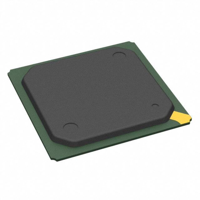
The SM712 is in a 256 BGA package.
Figure 2 illustrates the pinout diagram for SM712 256 BGA package. Figure 34 illustrates the mechanical dimensions of
the BGA package.
LynxEM+ Pin Descriptions
The following table, Table 2 provides brief description of each BGA ball of the LynxEM+. Signal names with ~ preceding
are active "LOW" signals, whereas signal names without ~ preceding are active "HIGH" signals. Also, the following
abbreviations are used for Pin Type.
Table 3 outlines the numerical SM712 BGA pins.
I
-
INPUT SIGNAL
O
-
Output Signal
I/O
-
Input or Output Signal
Note: All Outputs and I/O signals are tri-stated. Internal pull-up for I/O pad are all 100KΩ resistor, with the exception for
CPUCLK, which is 200KΩ resistor. Internal pull-down for I/O pad are all 100KΩ resistor.
Pins
2-1
�Silicon Motion®, Inc.
LynxEM+
DataBook
Table 2: Pin Description
Signal Name
Type
Pull-up/
Pull-Down
IOL
(mA)
Max. Load
(pF)
Description
Host Interface
AD [31:0]
I/O
16
120
PCI multiplexed Address and Data Bus. A bus transaction
consists of an address cycle followed by one or more data
cycles.
C/
~BE [3:0]
I/O
16
120
PCI Bus Command and Byte Enables. These signals carry
the bus command during the address cycle and byte enable
during data cycles.
PAR
I/O
16
120
Parity. LynxEM+ asserts this signal to verify even parity
across AD [31:0] and C/~BE [3:0].
~FRAME
I/O
16
120
Cycle Frame. LynxEM+ asserts this signal to indicate the
beginning and duration of a bus transaction. It is deasserted during the final data cycle of a bus transaction.
~TRDY
I/O
16
120
Target Ready. A bus data cycle is completed when both
~IRDY and ~TRDY are asserted on the same cycle.
~IRDY
I/O
16
120
Initiator Ready. A bus data cycle is completed when both
~IRDY and ~TRDY are asserted on the same cycle.
~STOP
I/O
16
120
Stop. LynxEM+ asserts this signal to indicate that the
current target is requesting the master to stop current
transaction.
~DEVSEL
I/O
16
120
Device Select. LynxEM+ asserts this signal when it
decodes its addresses as the target of the current
transaction.
IDSEL
I
ID Select. This input is used during PCI configuration
read/write cycles.
CLK
I
PCI System Clock, 33 MHz.
~RST
I
PCI System Reset. LynxEM+ asserts this signal to force
registers and state machines to initial default values
~REQ
O
~GNT
I
~INTA
O
8
120
PCI Bus Request (bus master mode)
PCI Bus Grant (bus master mode)
8
120
PCI Interrupt
Power Down Interface
~PDOWN
I
pull-up
Power down mode enable
~CLKRUN/
ACTIVITY
O
pull-up
REFCLK
I
pull-up
32 KHz refresh clock source for power down or PALCLK
for PALTV
CKIN
I
pull-up
14.318 MHz clock (~EXCKEN = 1) or Video Clock
(~EXCKEN = 0)
MCKIN/
LVDSCLK
I/O
pull-up
~EXCKEN
I
pull-up
4
60
~CLKRUN or LynxEM+ Memory and I/O activity
detection depending on SCR18 [7]
0 = select ~CLKRUN
1 = select ACTIVITY
Clock Interface
2-2
4
60
Memory Clock In (~EXCKEN = 0) or
LVDSCLK Out (~ESCKEN = 1), LVDSCLK is a free
running clock which can be used to drive LVDS
transmitter for DSTN panels.
60
External Clock Enable. Select external VCLK form CKIN
and MCLK from MCKIN.
Pins
�Silicon Motion®, Inc.
Signal Name
Type
LynxEM+
DataBook
Pull-up/
Pull-Down
IOL
(mA)
Max. Load
(pF)
Description
External Display Memory Interface
MA [9:0]
O
8
50
External Memory Address Bus. The video memory row
and column addresses are multiplexed on these lines.
MD [63:0]
I/O
pull-up
4
20
External Memory Data Bus
~WE
O
pull-up
8
50
External Memory Write Strobe
~RAS
O
pull-up
8
50
External Memory SDRAM Row Address Select
~CAS
O
pull-up
8
50
External SGRAM Column Address Select
~CS0
O
pull-up
8
50
External SGRAM Chip Select 0, select 1st 1MB within the
2MB memory, or select 1st 2MB within the 4MB memory
~DQM
[7:0]
O
pull-up
8
50
External SGRAM I/O mask [7:0]. DQM [7:0] are byte
specific. DQM0 masks MD [7:0], DQM1 masks MD
[15:8],Ö,and DQM7 masks MD [63:58].
DSF
O
pull-up
8
50
External SGRAM Block write
BA
O
8
50
External SGRAM Bank Select. SDRAM has dual internal
banks. Bank address defines to which bank the current
command is being applied.
SDCK
I/O
pull-up
16
50
External SGRAM clock. SDCK is driven by the memory
clock. All SDRAM input signals are sampled on the
positive edge of SDCK.
SDCKEN
I/O
pull-up
8
50
External SGRAM clock enable. SDCKEN activates
(HIGH) and deactivates (LOW) the SDCLK signal.
Deactivating the SDCK provides POWER-DOWN and
SELF-REFRESH mode.
~ROMEN
O
pull-up
4
20
ROM Enable
Flat Panel Interface
FDATA [23:0]
O
pull-down
6
50
Flat Panel Data bit 23 to bit 0. Note: For SM712, the upper
12 bits [25:24] are multiplexed with ZV port, and the
upper 12 bits [23:11] are dedicated for flat panel data
LP/FHSYNC
O
pull-down
6
50
DSTN LCD: Line Pulse
TFT LCD: LCD Horizontal Sync
FP/FVSYNC
O
pull-down
6
50
DSTN LCD: Frame Pulse
TFT LCD: LCD vertical sync
M/
DE
O
pull-down
6
50
M-signal or Display Enable. This signal is used to indicate
the active horizontal display time.
FPR3E [7] is used to select
1 = M-signal
0 = Display Enable
FPSCLK
O
pull-down
6
50
Flat Panel Shift Clock. This is the pixel clock for Flat
Panel Data.
FPEN
O
pull-down
4
20
Flat Panel Enable. This signal needs to become active after
all panel voltages, clocks, and data are supplied. This
signal also needs to become inactive before any panel
voltages or control signals are removed. FPEN is part of
the VESA FPDI-1B specification.
FPVDDEN
O
pull-down
4
20
Flat Panel VDD Enable. This signal is used to control
LCD logic power.
VBIASEN
O
pull-down
4
20
Flat Panel Voltage Bias Enable. This signal is used to
control LCD Bias power.
Pins
2-3
�Silicon Motion®, Inc.
Signal Name
Type
LynxEM+
DataBook
Pull-up/
Pull-Down
IOL
(mA)
Max. Load
(pF)
Description
CRT Interface
RED
O
Analog Red Current Output
GREEN
O
Analog Green Current Output
BLUE
O
Analog Blue Current Output
IREF
I
Current Reference Input
CRTVSYNCC
O
pull-up
6
50
CRT Vertical Sync
CRTHSYNC/
CSYNC
O
pull-up
6
50
CRT Horizontal Sync or Composite Sync depending on
CCR65 [0]
0 = CRT Horizontal Sync
1 = Composite Sync
4
20
RGB or YUV input/ RGB digital output
Video Port Interface
P [15:0]
I/O
PCLK
I/O
pull-up
4
20
Pixel Clock
VREF
I/O
pull-up
4
20
VSYNC input from PC Card or video decoder
HREF
I/O
pull-up
4
20
HSYNC input from PC Card or video decoder
BLANK/
TVCLK
I/O
pull-up
4
20
Blank output or TVCLK output depending on CCR69 bit
7.
0 = BLANK output
1 = TVCLK output
TVCLK output is used to drive external NTSC/PAL TV
encoder. To select NTSC or PAL TV, please refer to
CCR65 register
General Purpose Registers / I2C
USR3
I/O
pull-up
4
20
General Purpose register. It is recommended to use USR3
to control TV On/Off.
0 = TV display is OFF
1 = TV display is ON
USR2
I/O
pull-up
4
20
General Purpose register. It is recommended to use USR2
to select NTSC/PAL TV settings.
0 = PALTVCLK
1 = NTSCTVCLK or REFCLK
USR1 / SDA
I/O
pull-up
4
20
General Purpose register. USR1/ DDC2/ I2C Data. Can be
used to select different test modes.
USR0 / SCL
I/O
pull-up
4
20
General Purpose register. USR0/ DDC2/ I2C Clock. Can
be used to select different test modes.
I
pull-down
Test Mode Pins
TEST [1:0]
Test mode selects
VCC and GROUND Pins
HVDD
Host Interface VDD on I/O Ring, 3.3V
MVDD
Display Memory Interface VDD on I/O Ring, 3.3V
FPVDD
Flat Panel Interface VDD on I/O Ring, 3.3V
VPVDD
VPort Interface VDD on I/O Ring 3.3V
CVDD
Clock (PLL) Analog Power, 3.3V
AVDD
DAC Analog Power, 3.3V
2-4
Pins
�Silicon Motion®, Inc.
Signal Name
Type
LynxEM+
DataBook
Pull-up/
Pull-Down
IOL
(mA)
Max. Load
(pF)
Description
RVDD
RAM Filtered Palette Power, 3.3V
CVSS
PLL Analog Ground
AVSS1
DAC Analog Ground
AVSS2
DAC Analog Ground
RVSS
RAM Filtered Palette Ground
VDD
Digital 3.3V Core Power Supply
Digital 3.3V Internal Memory Power Supply
VSS
Digital Ground
Pins
2-5
�Silicon Motion®, Inc.
1
2
LynxEM+
DataBook
3
4
5
6
7
8
9
10
11
12
13
14
15
16
17
18
19
20
MD12
MD3
MD4
MD5
MD7
MD31
MD17
MD28
MD20
MD25
MD22
AD0
AD4
AD7
AD9
AD12
AD14
PAR
~FRAME
B
MD2
MD0
MD11
MD9
MD8
~DQM3
MD30
MD18
MD27
MD21
MD24
AD1
AD5
~BE0
AD10
AD13
~BE1
~TRDY
~STOP
AD16
B
C
MD15
MD1
MD13
MD10
MD6
~DQM2
MD16
MD29
MD19
MD26
MD23
AD3
AD6
AD8
AD11
AD15
~DEVSEL
~IRDY
AD17
AD18
C
D
N/C
~CS0
~DQM1
MD14
VDD
VSS
MVDD
N/C
MVDD
VSS
VSS
AD2
HVDD
VSS
HVDD
VDD
VSS
HVDD
AD19
AD20
AD21
D
E
~WE
BA
~DQM0
VSS
VSS
AD22
AD23
IDSEL
E
MA5
~CAS
~RAS
MVDD
HVDD
~BE3
AD24
AD25
F
G
MA7
MA3
MA4
VSS
VDD
AD26
AD27
AD28
G
H
MA1
MA8
MA2
MA6
VSS
AD29
AD30
AD31
H
J
SDCKEN
SDCK
MA9
MA0
HVDD
~REQ
~GNT
CLK
J
K
N/C
~ROMEN
DSF
VSS
~RST
~INTA
REFCLK
K
L
MD55
MD56
MD54
VSSA
MCKIN
~PDOWN
~CLKRUN
~EXCKEN
L
M
MD57
MD53
MD58
VDD
N/C
PALCLK
VREF
HREF
BLANK
M
N
MD52
MD59
MD51
VSS
P4
P1
P0
PCLK
N
P
MD60
MD50
MD61
MVDD
N/C
P5
P3
P2
P
R
MD49
MD62
MD48
~DQM7
VPVDD
P8
P7
P6
R
T
MD63
~DQM6
MD39
VSS
N/C
P12
P10
P9
T
U
MD40
MD38
MD41
MD43
MVDD
N/C
FDA22
N/C
FPVDD
N/C
N/C
FPVDD
N/C
FPVDDEN
CVSS
AVSS1
USR0
TEST1
P13
P11
U
V
MD37
MD42
MD34
MD33
~DQM5
FPSCLK
FDA23
FDA19
FDA16
FDA13
FDA8
FDA5
FDA2
VBIASEN
CVDD
RVSS
BLUE
USR1
TEST0
P14
V
W
MD36
MD46
MD45
MD47
LP
DE
FDA21
FDA18
FDA15
FDA12
FDA9
FDA6
FDA3
FDA0
CRTH
SYNC
RVDD
IREF
RED
P15
USR2
W
Y
MD35
MD44
MD32
~DQM4
FP
FPEN
FDA20
FDA17
FDA14
FDA11
FDA10
FDA7
FDA4
FDA1
CRTV
SYNC
CKIN
AVDD
GREEN
AVSS2
USR3
Y
16
17
18
19
A
F
1
2
3
SM712
TOP VIEW
N/C
4
5
6
7
8
9
10
11
12
13
14
15
~BE2
A
20
Figure 2: SM712 Pin Diagram for 256 BGA Package
N/C = Not Connected but compatible with SM810.
2-6
Pins
�Silicon Motion®, Inc.
LynxEM+
DataBook
Table 3: SM712 Pin Diagram for 256 BGA Package
#
SM712 Name
A1
MD12
{Function1}
{Function2}
{Function3}
{Function4}
VDD
A2
MD3
{ROM}
MVDD
A3
MD4
ROMD4
MVDD
A4
MD5
ROMD5
MVDD
A5
MD7
ROMD7
MVDD
A6
MD31
MVDD
A7
MD17
MVDD
A8
MD28
MVDD
MVDD
A9
MD20
MVDD
A10
MD25
MVDD
A11
MD22
MVDD
A12
AD0
HVDD
A13
AD4
HVDD
A14
AD7
HVDD
A15
AD9
HVDD
A16
AD12
HVDD
A17
AD14
HVDD
A18
PAR
HVDD
A19
~FRAME
HVDD
A20
C/~BE2
HVDD
B1
MD2
ROMD2
MVDD
B2
MD0
ROMD0
MVDD
B3
MD11
MVDD
B4
MD9
MVDD
B5
MD8
MVDD
B6
~DQM3
MVDD
B7
MD30
MVDD
B8
MD18
MVDD
B9
MD27
MVDD
B10
MD21
MVDD
B11
MD24
MVDD
B12
AD1
HVDD
B13
AD5
HVDD
B14
C/~BE0
HVDD
B15
AD10
HVDD
B16
AD13
HVDD
B17
C/~BE1
HVDD
B18
~TDRY
HVDD
B19
~STOP
HVDD
B20
AD16
HVDD
C1
MD15
MVDD
Pins
2-7
�Silicon Motion®, Inc.
LynxEM+
DataBook
#
SM712 Name
{Function1}
{Function2}
{Function3}
{Function4}
VDD
C2
MD1
ROMD1
C3
MD13
C4
MD10
C5
MD6
C6
~DQM2
MVDD
C7
MD16
MVDD
C8
MD29
MVDD
C9
MD19
MVDD
C10
MD26
MVDD
C11
MD23
MVDD
C12
AD3
HVDD
C13
AD6
HVDD
C14
AD8
HVDD
C15
AD11
HVDD
C16
AD15
HVDD
C17
~DEVSEL
HVDD
C18
~IDRY
HVDD
C19
AD17
HVDD
C20
AD18
HVDD
D1
N/C
MVDD
D2
~DQM1
MVDD
D3
MD14
MVDD
D4
VDD
D5
VSS
D6
MVDD
D7
N/C
D8
MVDD
D9
VSS
D10
VSS
D11
AD2
D12
HVDD
D13
VSS
D14
HVDD
D15
VDD
MVDD
MVDD
MVDD
ROMD6
MVDD
HVDD
D16
VSS
D17
HVDD
D18
AD19
HVDD
D19
AD20
HVDD
D20
AD21
HVDD
E1
~WE
MVDD
E2
BA
MVDD
E3
~DQM0
MVDD
2-8
Pins
�Silicon Motion®, Inc.
#
SM712 Name
E4
VSS
E17
VSS
LynxEM+
DataBook
{Function1}
{Function2}
{Function3}
{Function4}
VDD
E18
AD22
HVDD
E19
AD23
HVDD
E20
IDSEL
HVDD
F1
MA5
MVDD
F2
~CAS
MVDD
F3
~RAS
MVDD
F4
MVDD
F17
HVDD
F18
C/~BE3
HVDD
F19
AD24
HVDD
F20
AD25
HVDD
G1
MA7
MVDD
G2
MA3
MVDD
G3
MA4
MVDD
G4
VSS
G17
VDD
G18
AD26
HVDD
G19
AD27
HVDD
G20
AD28
HVDD
H1
MA1
MVDD
H2
MA8
MVDD
H3
MA2
MVDD
H4
MA6
MVDD
H17
VSS
H18
AD29
HVDD
H19
AD30
HVDD
H20
AD31
HVDD
J1
SDCKEN
MVDD
J2
SDCK
MVDD
J3
MA9
MVDD
J4
MA0
MVDD
J17
HVDD
J18
~REQ
HVDD
J19
~GNT
HVDD
J20
CLK
HVDD
K1
NC
K2
~ROMEN
MVDD
K3
DSF
MVDD
K4
N/C
K17
VSS
Pins
2-9
�Silicon Motion®, Inc.
LynxEM+
DataBook
#
SM712 Name
{Function1}
{Function2}
{Function3}
{Function4}
VDD
K18
~RST
HVDD
K19
~INTA
HVDD
K20
REFCLK
HDD
L1
MD55
MVDD
L2
MD56
MVDD
L3
MD54
MVDD
L4
VSS
L17
MCKIN/LVDSCK
L18
~PDOWN
HVDD
L19
~CLKRUN /
ACTIVITY
HVDD
L20
~EXCKEN
HVDD
M1
MD57
MVDD
M2
MD53
MVDD
M3
MD58
MVDD
M4
VDD
M17
N/C
{ZV IN}
{TESTMODE1}
{VP OUT}
M18
VREF
VS
TD19
R2
VPVDD
M19
HREF
HREF
{External TV
encoder}
TD18
R3
VPVDD
M20
BLANK/TVCLK
TVCLK
TD17
BLANK
VPVDD
N1
MD52
MVDD
N2
MD59
MVDD
N3
MD51
N4
VSS
N17
P4
UV4
Ge4
TD4
B3
VPVDD
N18
P1
UV1
Be5
TD1
B6
VPVDD
Be4
MCKIN
LVDSCK
HVDD
MVDD
{TFT 18x2}
N19
P0
UV0
N20
PCLK
PCLK
TD0
B7
VPVDD
TD16
PCLK
VPVDD
P1
MD60
MVDD
P2
MD50
MVDD
P3
MD61
MVDD
P4
MVDD
P17
N/C
{ZV IN}
P18
P5
UV5
Ge5
TD5
B2
VPVDD
P19
P3
UV3
Bo5
TD3
B4
VPVDD
P20
P2
UV2
Bo4
TD2
B5
VPVDD
R1
MD49
MVDD
R2
MD62
MVDD
R3
MD48
MVDD
2 - 10
Pins
�Silicon Motion®, Inc.
#
SM712 Name
R4
~DQM7
R17
VPVDD
LynxEM+
DataBook
{Function1}
{Function2}
{Function3}
{Function4}
VDD
MVDD
R18
P8
Y0
Re4
TD8
G5
VPVDD
R19
P7
UV7
Go5
TD7
G6
VPVDD
R20
P6
UV6
Go4
TD6
G7
VPVDD
T1
MD63
T2
~DQM6
{ROM}
MVDD
T3
MD39
ROMA7
MVDD
T4
VSS
T17
N/C
MVDD
{ZV IN}
T18
P12
Y4
TD12
R7
VPVDD
T19
P10
Y2
Ro4
TD10
G3
VPVDD
T20
P9
Y1
Re5
TD9
G4
VPVDD
{ROM}
U1
MD40
ROMA8
MVDD
U2
MD38
ROMA6
MVDD
U3
MD41
ROMA9
MVDD
U4
MD43
ROMA11
MVDD
U5
MVDD
U6
N/C
{DSTN}
U7
FDATA22
UD10
U8
N/C
RB5
Ro2
R6
FPVDD
RB4
U9
FPVDD
U10
N/C
GB4
U11
N/C
BB5
U12
FPVDD
U13
N/C
U14
FPVDDEN
BA4
U15
CVSS
U16
AVSS1
{I2C/DDC}
{USR CFG}
U17
USR0/SCL
SCL (Prim)
USR0
U18
TEST1
{ZV IN}
U19
P13
Y5
{TFT18x2}
TD13
R6
VPVDD
U20
P11
Y3
Ro5
TD11
G2
VPVDD
V1
MD37
ROMA5
MVDD
V2
MD42
ROMA10
MVDD
V3
MD34
ROMA2
MVDD
V4
MD33
ROMA1
MVDD
V5
~DQM5
{DSTN}
MVDD
V6
FPSCLK
XCK
V7
FDATA23
UD11
VPVDD
TEST1
VPVDD
{ROM}
Pins
Ro3
CK
FPVDD
R7
FPVDD
2 - 11
�Silicon Motion®, Inc.
LynxEM+
DataBook
#
SM712 Name
{Function1}
{Function2}
V8
FDATA19
UD7
V9
FDATA16
V10
V11
{Function3}
{Function4}
VDD
Re3
R3
FPVDD
UD4
Re0
R0
FPVDD
FDATA13
UD1
Go1
G5
FPVDD
FDATA8
LD8
Ge0
G0
FPVDD
V12
FDATA5
LD5
Bo1
B5
FPVDD
V13
FDATA2
LD2
Be2
B2
FPVDD
V14
VBIASEN
V15
CVDD
FPVDD
V16
RVSS
V17
BLUE
{I2C/DDC}
{USR CFG}
V18
USR1/SDA
SDA (Prim)
USR1
V19
TEST0
{ZV IN}
TEST0
V20
P14
Y6
TD14
VPVDD
VPVDD
R5
VPVDD
{ROM}
W1
MD36
ROMA4
MVDD
W2
MD46
ROMA14
MVDD
W3
MD45
ROMA13
MVDD
W4
MD47
ROMA15
MVDD
W5
LP/ FHSYNC
LP
FHSYNC
FPVDD
W6
M/ DE
M/DE
DE
FPVDD
W7
FDATA21
UD9
R5
FPVDD
W8
FDATA18
UD6
Re2
R2
FPVDD
W9
FDATA15
UD3
Go3
G7
FPVDD
W10
FDATA12
UD0
Go0
G4
FPVDD
W11
FDATA9
LD9
Ge1
G1
FPVDD
W12
FDATA6
LD6
Bo2
B6
FPVDD
W13
FDATA3
LD3
Be3
B3
FPVDD
W14
FDATA0
LD0
Be0
B0
FPVDD
{DSTN}
Ro1
{External TV
encoder}
W15
CSYNC
CSYNC
W16
RVDD
W17
IREF
W18
RED
W19
P15
{ZV IN}
Y7
2C/DDC}
{I
W20
USR2
VPVDD
SCL
TD15
R4
VPVDD
{USR CFG}
USR2/NTSCPAL
VPVDD
{ROM}
Y1
MD35
ROMA3
MVDD
Y2
MD44
ROMA12
MVDD
2 - 12
Pins
�Silicon Motion®, Inc.
LynxEM+
DataBook
#
SM712 Name
{Function1}
{Function2}
Y3
MD32
ROMA0
Y4
~DQM4
{DSTN}
Y5
FP/ FVSYNC
FP
Y6
FPEN
FPEN
{TFT 18x2}
Y7
FDATD20
UD8
Y8
FDATA17
{Function3}
{Function4}
VDD
MVDD
{TFT}
MVDD
FVSYNC
FPVDD
FPEN
FPVDD
Ro0
R4
FPVDD
UD5
Re1
R1
FPVDD
Y9
FDATA14
UD2
Go2
G6
FPVDD
Y10
FDATA11
LD11
Ge3
G3
FPVDD
Y11
FDATA10
LD10
Ge2
G2
FPVDD
Y12
FDATA7
LD7
Bo3
B7
FPVDD
Y13
FDATA4
LD4
Bo0
B4
FPVDD
Y14
FDATA1
LD1
Be1
B1
FPVDD
Y15
CRTVSYNC
Y16
CKIN
FPVDD
Y17
AVDD
Y18
GREEN
Y19
AVSS2
{I2C/DDC2}
{USR CFG}
Y20
USR3
SDA
USR3/
TVONOFF
Pins
VPVDD
2 - 13
�Silicon Motion®, Inc.
LynxEM+
DataBook
LynxEM+ NAND Tree Scan Testing
The LynxEM+ NAND Tree scan test circuit is designed for verifying the device being properly soldered to the board. It
detects opened/shorted traces of a signal pin with a simple test pattern which, for this particular case, only ~200 vectors in
length. The NAND Tree scan test circuit uses Combinational logic; therefore, no clock pulses are required during the
testing.
General Information
The LynxEM+ NAND Tree scan test circuit is a long chain of 2-input NAND gates. The first pin of the NAND chain is an
input (signal pin "MCKIN"), the last pin of the chain is an output (signal pin "BLANK"). In order to setup LynxEM+ for
NAND Tree scan testing, program USR[3:0] pins to 0011h and Test[1:0] pins to 10h. ALL VDD's, VSS's, and Analog
pins RED, GREEN, BLUE, IREF, and Control pins USR[3:0], Test[1:0] are not included in the scan chain.
NAND Tree
Pad_output
Nandtree_en pad_input 1
pad_input 2
pad_input 3
pad_input N
Figure 3: NAND Tree Connection
Table 4: NAND Tree Scan Test Order
Nand Tree Scan
Pin Order #
Pin Name
In/Out
1
MCKIN
In
2
~PDOWN
In
3
ACTIVITY
In
4
EXCKEN
In
5
REFCLK
In
6
~INTA
In
7
~RST
In
2 - 14
8
CLK
In
9
~GNT
In
10
~REQ
In
11
AD31
In
12
AD30
In
13
AD29
In
14
AD28
In
15
AD27
In
16
AD26
In
17
AD25
In
18
AD24
In
Pins
�Silicon Motion®, Inc.
Pins
LynxEM+
DataBook
Nand Tree Scan
Pin Order #
Pin Name
19
~CBE3
In
20
IDSEL
In
21
AD23
In
22
AD22
In
23
AD21
In
24
AD20
In
25
AD19
In
26
AD18
In
27
AD17
In
28
AD16
In
29
CBE2
In
30
~FRAME
In
31
~IRDY
In
32
~TRDY
In
33
~DEVSEL
In
34
~STOP
In
35
PAR
In
36
~CBE1
In
37
AD15
In
38
AD14
In
39
AD13
In
40
AD12
In
41
AD11
In
42
AD10
In
43
AD9
In
44
AD8
In
45
~CBE0
In
46
AD7
In
47
AD6
In
48
AD5
In
49
AD4
In
50
AD3
In
51
AD2
In
52
AD1
In
53
AD0
In
54
MD23
In
55
MD24
In
56
MD22
In
57
MD25
In
58
MD21
In
59
MD26
In
In/Out
2 - 15
�Silicon Motion®, Inc.
LynxEM+
DataBook
Nand Tree Scan
Pin Order #
Pin Name
In/Out
60
MD20
In
61
MD27
In
62
MD19
In
63
MD28
In
64
MD18
In
65
MD29
In
66
MD17
In
67
MD30
In
68
MD16
In
69
MD31
In
70
DQM3
In
71
DQM2
In
72
MD7
In
73
MD8
In
74
MD6
In
75
MD9
In
76
MD5
In
77
MD10
In
78
MD4
In
79
MD11
In
80
MD3
In
81
MD12
In
82
MD2
In
83
MD13
In
84
MD1
In
85
MD14
In
86
MD0
In
87
MD15
In
88
DQM1
In
89
DQM0
In
90
BA
In
91
~WE
In
92
~RAS
In
93
~CAS
In
94
MA5
In
95
MA4
In
96
MA6
In
97
MA3
In
98
MA7
In
99
MA2
In
100
MA8
In
2 - 16
Pins
�Silicon Motion®, Inc.
Pins
LynxEM+
DataBook
Nand Tree Scan
Pin Order #
Pin Name
In/Out
101
MA1
In
102
MA9
In
103
MA0
In
104
SDCK
In
105
SDCKEN
In
106
DSF
In
107
~ROMEN
In
108
~CS0
In
109
MD55
In
110
MD56
In
111
MD54
In
112
MD57
In
113
MD53
In
114
MD58
In
115
MD52
In
116
MD59
In
117
MD51
In
118
MD60
In
119
MD50
In
120
MD61
In
121
MD49
In
122
MD62
In
123
MD48
In
124
MD63
In
125
DQM7
In
126
DQM6
In
127
MD39
In
128
MD40
In
129
MD38
In
130
MD41
In
131
MD37
In
132
MD42
In
133
MD36
In
134
MD43
In
135
MD35
In
136
MD44
In
137
MD34
In
138
MD45
In
139
MD33
In
140
MD46
In
141
MD32
In
2 - 17
�Silicon Motion®, Inc.
Nand Tree Scan
Pin Order #
2 - 18
LynxEM+
DataBook
Pin Name
In/Out
142
MD47
In
143
DQM5
In
144
DQM4
In
145
FHSYNC
In
146
FVSYNC
In
147
FPSCLK
In
148
DE
In
149
FPEN
In
150
FDATA23
In
151
FDATA22
In
152
FDATA21
In
153
FDATA20
In
154
FDATA19
In
155
FDATA18
In
156
FDATA17
In
157
FDATA16
In
158
FDATA15
In
159
FDATA14
In
160
FDATA13
In
161
FDATA12
In
162
FDATA11
In
163
FDATA10
In
164
FDATA9
In
165
FDATA8
In
166
FDATA7
In
167
FDATA6
In
168
FDATA5
In
169
FDATA4
In
170
FDATA3
In
171
FDATA2
In
172
FDATA1
In
173
FDATA0
In
174
FPVDDEN
In
175
VBIASEN
In
176
CRTVSYNC
In
177
CRTHSYNC
In
178
P15
In
179
P14
In
180
P13
In
181
P12
In
182
P11
In
Pins
�Silicon Motion®, Inc.
Pins
LynxEM+
DataBook
Nand Tree Scan
Pin Order #
Pin Name
In/Out
183
P10
In
184
P9
In
185
P8
In
186
P7
In
187
P6
In
188
P5
In
189
P4
In
190
P3
In
191
P2
In
192
P1
In
193
P0
In
194
PCLK
In
195
VREF
In
196
HREF
In
197
BLANK
Out
2 - 19
��Silicon Motion®, Inc.
LynxEM+
DataBook
Chapter 3: Initialization
LynxEM+ generates an internal power-on reset during system power-on. After receiving the system ~RESET signal,
LynxEM+ will release its internal power-on reset circuit and enter the RESET period until the host de-asserts the ~RESET
signal. During the RESET period, LynxEM+ resets its internal state machines and registers to the power-on default states.
During power-on, LynxEM+ is configured based on configuration lines MD [22:0].
Table 5 (see end of this section) provides a detailed description of each configuration line. All MD (memory data) lines
have internal pull-up resistors on I/O pads which are latched into the corresponding register as logic "1" on the rising edge
(trailing edge) of the ~RESET. To set a specific bit as logic "0" during power-on reset, an external pull-down resistor must
be added on the corresponding MD line.
In addition to power-on configuration, LynxEM+ performs an initialization sequence for the 2MB or 4MB of internal
memory.
Figure 4 illustrates the power-up sequence.
•
•
•
•
•
DQM and SDCKEN signals go HIGH, initially tracking VCC.
200ms delay
PRECHARGE command for all banks
LOAD MODE REGISTER command
8 AUTO REFRESH cycles
After memory initialization has been completed, LynxEM+'s video BIOS is ready to service system BIOS requests.
System BIOS passes a pointer to the LynxEM+ video BIOS to start the video BIOS initialization sequence.
SDCK
SDCKEN
COMMAND
NOP
MA
MD
PRECHARGE
LOAD MODE
REGISTER
BOTH
BANKS
CODE
NOP
AUTO
REFRESH
NOP
AUTO
REFRESH
NOP
ACTIVE
BANK ROW
High-Z
T=200us
POWER-UP
VCC and
SDCLK stable
tRP
PRECHARGE
tMTC
Program Mode Register
tRC
1st AUTO REFRESH Cycle
tRC
8th AUTO REFRESH Cycle
Figure 4: External SGRAM Power-Up and Initialization Sequence
Initialization
3-1
�Silicon Motion®, Inc.
LynxEM+
DataBook
Figure 5 illustrates the LynxEM+ Video BIOS initialization flow. The initialization sequence consists of the following
stages:
•
•
•
•
•
Determine memory size
Check for display type. (FPR31 [2:0]) LCD only, CRT only, LCD and CRT or LCD and TV, etc.
Program the appropriate timing registers based on the display type
Set to mode 3h to display characters on the display for users to read
Pass the pointer back to system BIOS
Start
Turn off display 3C5.1=20h
Unlock extended reg 3C3=40h
yes
CFG_Flag
no
Over-write
MD lines
Int 15 Panel ID
no
yes
Write MD[19:16] based on Panel ID
Read MD settings
Determine memory size
Determine panel size and type
initialize panel
(load FPR30,32,34-57)
Load CFG table
(set MCLK, scratch-bits, etc.)
Initialize INT 10h
Initialize BIOS data area
Set mode 3
Turn on display by setting FPR31
Display banner
Done
Figure 5: LynxEM+ BIOS Initialization Flowchart
3-2
Initialization
�Silicon Motion®, Inc.
LynxEM+
DataBook
LynxEM+ Power-On Configurations
•
•
•
All MD (memory data) lines have internal pull-up resistors on I/O pads.
0 = external pull-down resistor (recommended value is 1K ohm)
1 = no external pull-down resistor
Table 5: Power-On Configurations
Signal Name
Read/Write
Register Bits
Address
CPR00 [25]
LynxEM+ Description
MD [23]
R
0 = External memory access only
1 = Allows both internal and external memory access
(default)
MD [22]
CONFIG
ONLY
0 = 32K
1 = 64K BIOS size default
MD [21] 1
CONFIG
ONLY
EBROM Generate
0 = EBROM
1 = no EBROM (default)
MD [20] 1
CONFIG
ONLY
Expansion ROM
0 = Expansion ROM
1 = no Expansion ROM (default)
MD [19:16]
R/W
GPR70 [3:0]
3C5h.70
User configuration Bits
MD15
R/W
FPR30 [7]
3C5h.30
DSTN Interface Type
0 = 16-bit interface
1 = 24-bit interface
MD [14:12]
R/W
FPR30 [6:4]
3C5h.30
Color TFT Interface Type
000 = 9-bit, 3-bit per R, G, B
001 = 12-bit, 4-bit per R, G, B
010 = 18-bit, 6-bit per R, G, B
011 = 24-bit, 8-bit per R, G, B
100 = 24-bit, (12+12-bit, 2 pixels/clock)
101 = Analog TFT w/ analog R, G, B interface
110 = 36-bit, (18+18-bit, 2 pixels/clock)
MD [11:10]
R/W
FPR30 [3:2]
3C5h.30
LCD Display Size
00 = 640 x 480
01 = 800 x 600
10 = 1024 x 768
MD9
R/W
FPR30 [1]
3C5h.30
TFT FPCLK Select
0 = Normal
1 = Inverted
MD8
R/W
FPR30 [0]
3C5h.30
Color LCD Type
0 = color TFT
1 = color STN
MD7
R/W
MCR62 [7]
3C5h.62
Internal Logic
0 = Internal logic will be running 1/2X MCLK
1 = Internal logic will be running 1X MCLK
MD6
R/W
MCR62 [6]
3C5h.62
Enable Memory Data Bus
0 = Enable 32-bit memory data bus
1 = Enable 64-bit memory data bus
MD [5:4]
R/W
MCR62 [5:4]
3C5h.62
External SGRAM Memory Column Address Select
11 = 8-bit column address
10 = 9-bit column address
0x = 10-bit column address
Memory Pre-charge Timing Select
Reserved
Initialization
3-3
�Silicon Motion®, Inc.
Signal Name
Read/Write
LynxEM+
DataBook
Register Bits
Address
LynxEM+ Description
MD2
R/W
MCR62 [2]
3C5h.62
External Memory Enable
0 = Enable external 32-bit memory
1 = Disable external 32-bit memory
MD1
R/W
MCR62 [1]
3C5h.62
External SGRAM Memory Active-to-Precharge
Delay Select
0 = 7 MCLK
1 = 6 MCLK
MD0
R/W
MCR62 [0]
3C5h.62
External SGRAM Memory Refresh to Command
Delay
0 = 10 MCLK
1 = 9 MCLK
3-4
Initialization
�Silicon Motion®, Inc.
LynxEM+
DataBook
Chapter 4: PCI Bus Interface
LynxEM+ provides a glue-less interface to the PCI system bus, and the PCI Host Interface Unit supports burst read and
burst write for master mode and burst write for slave mode. To maximize performance, the Host Interface unit also
supports burst write and burst read with Read Look Ahead. The LynxEM+ is fully compliant with PCI Verison 2.1, but
does not have 5V tolerant I/O cell. If the LynxEM+ is used with 5V PCI then it will need an external glue-logic.
The LynxEM+'s PCI Host Interface Unit manages data transfer between the external PCI bus and internal Host Interface
(HIF) bus. All functional blocks, with the exception of the Drawing Engine, are tied to the HIF bus through a proprietary
protocol. Separate decode logic and a dedicated FIFO are used for the Drawing Engine.
In addition to PCI Configuration Space Registers, the PCI Host Interface Unit contains Power Down Control Registers
(PDR20-PDR23) and System Control Registers (SCR10-SCR1A). These Registers may accessed by the CPU even while
internal PLLs are turned off.
PCI Configuration Registers
The PCI configuration registers are designated CSR00 - CSR3D. A brief description of key elements of the register set
follows:
•
•
•
•
•
•
Vendor ID register (CSR00) - hardwired to 126Fh to identify Silicon Motion, Inc. as the chip vendor.
Device ID register (CSR02) - hardwired to 0810h to identify the LynxEM+ device. The ~DEVSEL timing in the
Status register (CSR06) - hardwired to 01b, which indicates medium speed for ~DEVSEL.
Class Code register (CSR08) - hardwired to 030000h to specify LynxEM+ as a VGA compatible device. Bit [7:0]
used to identify the revision of the LynxEM+.
Memory Base Address register (CSR10) - specifies the PCI configuration space for address relocation. After poweron, the register defaults to 00h, which indicates the base register can be located anywhere in a 32-bit address space
and that the base register is located in memory space.
Subsystem Vendor ID and Subsystem ID (addressable at CSR2C and CSR2E respectively) - 32-bit read only
registers. These registers are used to differentiate between multiple graphics adapters within the same system.
PCI Bus Interface
4-1
��Silicon Motion®, Inc.
LynxEM+
DataBook
Chapter 5: Display Memory Interface
Memory Configuration
The LynxEM+ supports a 2 or 4 Mbytes of memory. There are three memory configurations:
1.
2.
2 Mbytes internal memory only
4 Mbytes of internal memory (there is no option for external memory with this configuration)
The internal memory is 2 or 4 Mbytes of 512Kx32 SGRAM. The LynxEM+ single cycle interface may be clocked up to
129 MHz, which provides over 516 MB/s. The LynxEM4+ single cycle interface may be clocked up to 86 MHz, which
provides over 688 MB/s.
The LynxEM+ supports a total 2 Mbytes external memory composed of 256Kx32 SGRAM.
Page Break Look Ahead
For standard architectures, the memory controller will break cycle when the bus agent changes. LynxEM+ can allow a
"No Wait Cycle" during agent changes if the preceding and current agents are in the same page. Both the internal memory
bus and external memory bus support this capability.
Memory Timing Control
Memory timing control is configurable via MD[7:0] during power-on reset. See Table 5 in the Initialization section for a
complete description of these memory configuration bits.
Note:
All MD lines have internal pull-up resistors on I/O pads. The default configuration is therefore a logical "1" during power-on
reset. To set an MD line to 0, an external pull-down resistor needs to be added. After power-on initialization, software can be
used to overwrite the initial setting by writing to MCR62 -- bits 7-0 correspond to MD[7:0].
Display Memory Interface
5-1
��Silicon Motion®, Inc.
LynxEM+
DataBook
Chapter 7: Video Processor
LynxEM+'s Video Processor manages video data streams, as well as graphics data streams in non-VGA modes. The Video
Processor can process two independent video data streams. The two video windows (primary and secondary) can be
displayed at any screen location with any size, and can be overlaid with graphics data.
Within the Video Processor, the Graphics Source Control block, Video Window I Control block, Video Window II Control
block, and HW Pop-up Icon Control block all have independent Starting Address and Offset Address registers. This
means that each control block can fetch data from any display memory location. Video Window I source control block
supports double-buffered video capture. Internal logic automatically detects the control/status bits of the two capture
buffers and fetches the captured video data from the buffer which is not used.
The Video Processor supports TV flicker reduction for direct color modes (64K colors or 16M colors), as well as index
color modes (256 colors and 16 colors). A special data path is designed to feed the outputs of the color palette RAM back
to the TV Flicker Reduction block. The TV Overscan & Underscan Control block is used to convert 480 lines into 400
visible lines on NTSC TV display. The same function can also be used on PAL TV display. When the TV display is
enabled, the Shadow registers need to be locked as 640 x 480 mode (or 720 x 525 for PAL).
From VGA Core
8
8
HW Pop-Up
Icon Control
TV
Flicker
Reduction
Display
Memory
64
Graphics Source
Control
64
Video Window I
Source Control
To
Multimedia
RAMDAC
Block
TV
Overscan
&
Underscan
Control
24
Color
Key
Horizontal
Color Interpolation & Scaling
64
Video Window II
Source Control
Display
Control
YUV
to
RGB
Vertical
Color Interpolation & Scaling
Figure 6: Video Processor Block Diagram
Video Processor
7-1
��Silicon Motion®, Inc.
LynxEM+
DataBook
Chapter 6: Drawing Engine
LynxEM+'s Drawing Engine is designed to accelerate Microsoft's DirectDraw applications. The engine contains a 3operand ALU with 256 raster operations, source and destination FIFOs, as well as a host data FIFO. The drawing engine
pipeline allows single cycle operations and runs at the memory clock speed.
LynxEM+'s Drawing Engine includes several key functions to achieve the high GUI performance. The device supports
color expansion with packed mono font, color pattern fill, host BLT, stretch BLT, short stroke, line draw, and others.
Dedicated pathways are designed to transfer data between host interface (HIF) bus and Drawing Engine, and memory
interface (MIF) bus and Drawing Engine. In addition, the drawing engine supports rotation BIBLT for any block size, and
automatic self activate rotation BLIT. This feature allows conversion between landscape and portrait display without the
need for special software drivers.
LynxEM+ also supports fast DMA BLT, source clear during BLT, transparent BLT, programmable blter stride, page flip,
and current scan line refresh.
LynxEM+'s Drawing Engine is also used to bus master captured data to the hard disk drive or to system memory during
video capture. To accomplish this, the video capture driver turns on the Drawing Engine Capture Enable bit (DPR0E bit4),
selects HOST BLT Read command function (DPR0E [3:0]), and enables PCI bus master mode (SCR17 bit 6). The Video
Capture Unit loads the incoming video stream into Capture Buffer 1 or 2, depending on which is idle (VPR3C bit 1 or bit
2 = 0 indicates idle status). The Drawing Engine resets Capture Buffer I or Capture Buffer II control/Status bit to 0
(VPR3C bit 1 or bit 2) after a transfer has completed.
Drawing Engine
6-1
��Silicon Motion®, Inc.
LynxEM+
DataBook
Chapter 8: Zoom Video Port and Video Capture Unit
Zoom Video Port
LynxEM+'s Zoom Video Port (ZV Port) is designed to interface with video solutions implemented as PCMCIA (or PC
CardBus) cards: examples are NTSC/PAL decoders, MPEG-2 decoders, and JPEG Codecs. The ZV Port can also directly
interface with an NTSC/PAL decoder, such as Phillips 7111 or BT819. Figure 7 illustrates an example of the Phillips
video encoder interface via the ZV Port.
Incoming video data from the ZV Port interface can be YUV or RGB format. The data can be interlaced or noninterlaced. The ZV Port can be configured for output if the video capture function is disabled. 18-bit graphics and video
data in RGB format can be sent out when the ZV Port is configured for output mode.
The ZV Port may also be configured as a test port. Up to 20 signals from each of the logic blocks within the LynxEM+ can
be brought out to an internal test bus (TD Bus) connected to the ZV Port. System designers or silicon validation engineers
can access these signals by setting the TEST0, TEST1, USR0, USR1, and USR2 pins. This approach can bring out a total
of 180 internal signals to the primary I/O pins. The test port capability can be used to enhance fault coverage, as well as
reduce silicon validation or debugging time.
Table 6 lists signal definitions for the following ZV Port interface configurations: YUV input mode, RGB input mode, and
graphics/video (output mode).
Philips SAA7110/
SAA7111
Video
NTSC/PAL
RF Signal
LynxEM+
Y [7:0]
Y [7:0]
UV[7:0]
UV[7:0]
HREF
HREF
VS
VREF
LLC
PCLK
SDA
SDA
SCL
SCL
Figure 7: Video Encoder Interface via Video Port
Zoom Video Port and Video Capture Unit
8-1
�Silicon Motion®, Inc.
LynxEM+
DataBook
Table 6: LynxEM+ Video Port Interface I/O Configurations
Video Port Interface
ZV Port
(Input mode)
I/O
NTSC/PAL
Decoder (Input mode)
I/O
Graphics/Video
(Output mode)
I/O
VREF
VS
I
VS
I
R2
O
HREF
HREF
I
HREF
I
R3
O
BLANK
(note1)
BLANK
O
PCLK
PCLK
I
PCLK
I
PCLK
O
P15
UV7
I
R7
I
R4
O
P14
UV6
I
R6
I
R5
O
P13
UV5
I
R5
I
R6
O
P12
UV4
I
R4
I
R7
O
P11
UV3
I
R3
I
G2
O
P10
UV2
I
G7
I
G3
O
P9
UV1
I
G6
I
G4
O
P8
UV0
I
G5
I
G5
O
P7
Y7
I
G4
I
G6
O
P6
Y6
I
G3
I
G7
O
P5
Y5
I
G2
I
B2
O
P4
Y4
I
B7
I
B3
O
P3
Y3
I
B6
I
B4
O
P2
Y2
I
B5
I
B5
O
P1
Y1
I
B4
I
B6
O
P0
Y0
I
B3
I
B7
O
(note1)
Note 1: BLANK pin can used as TVCLK output, which is independent of ZV port.
Video Capture Unit
The Video Capture Unit captures incoming video data from the ZV Port and then stores the data into the frame buffer.
The Video Capture Unit support several features to maintain display quality, and balance the capture rate:
•
•
•
•
•
•
•
2-tap, 3-tap, and 4-tap horizontal filtering
2 to 1 and 4 to 1 reduction for horizontal and vertical frame size
YUV 4:2:2, YUV 4:2:2 with byte swap, RGB 5:5:5, and RGB 5:6:5
Multiple frame skipping methods
Interlaced data and non-interlaced data capture
Single buffer and double buffer capture
Cropping
LynxEM+ uses the Video Processor block to display the captured data on the LCD, TV, or CRT display. The captured data
can be displayed through Video Window I or Video Window II. The stretching, color interpolation, YUV-to-RGB
conversion, and color key functions are performed in the Video Processor. LynxEM+'s Video Processor can
simultaneously process captured video data and perform CD-ROM playback on two independent video windows.
LynxEM+ also supports real-time video capture to the hard drive or system memory through PCI master mode or slave
mode. In PCI bus master mode, LynxEM+ uses the Drawing Engine's Host BLT and Host DMA functions to maximize
performance.
8-2
Zoom Video Port and Video Capture Unit
�Silicon Motion®, Inc.
LynxEM+
DataBook
Functional Description
LynxEM+'s Video Capture Unit supports the Video Port Extension (VPE) specification for video stream processing. This
capture unit includes CLIP block, FILTER block, SHRINK block, and FIFO control block. Figure 8 and Figure 9 illustrate
the LynxEM+ Video Capture Block Diagram and Data Flow. The CLIP functional block is used to select the desired
rectangles from the video stream to be captured. VPR40 register (Video Source Clipping Control) is used to define the
upper left corner of the rectangle from the video source. VPR44 register (Video Source Capture Size Control) is used to
define the height and width of the rectangle from the video source.
Video Stream from
ZV Port
Display Memory
CLIP
On Screen
Graphics
FILTER
SHRINK
Capture Buffer I
VPR48
FIFO
Capture Buffer II
Drawing
Engine
PCI Bus
Interface
Block
VPR1C
Video
Window I
VPR30
Video
Window II
VPR4C
Figure 8: Video Capture Block Diagram
The FILTER functional block controls horizontal filtering logic. VPR3C (Capture Port Control) bit 21 and bit 20 are used
to select 2 tap, 3 tap, and 4 tap filtering. The SHRINK functional block is used to not only reduce the storage area for both
display memory and hard drive, but also increase performance of video capture and video playback. VPR3C bit 19 and 18
are used to enable vertical reduction, and bit 17 and bit 16 are used to enable horizontal reduction. With filter and shrink
functions, LynxEM+ is able to achieve high video capture performance and maintain optimal video playback quality.
VPR3C bit 13 to bit 11 are use to select 8 different frame skipping options in the event the capture rate is less than the
incoming video stream. CPR00 bit 10 and bit 9 are used to support interlaced capture and double buffer capture. CPR00
bit 1 and bit 2 are used as control/status bits for Buffer I and Buffer II.
The captured data can be displayed on either Video Window I or Video Window II. The video capture driver needs to
program VPR1C (or VPR30), Video Window I (or II) Source Start Address, with the same address value from Capture
Port Buffer I or II Start Address register. VPR00 (Miscellaneous Graphics and Video Control) bit 24 may be used to
automatically display the capture data on Video Window I without programming VPR1C register. This feature is
independent of single buffer or double buffer mode. If double buffer mode is at Video Window I, it will display the buffer
which is not currently used to capture data. This feature allows the user to capture interlaced data and together with
programming VPR24 bit [23:16] and VPR24 bit [31:24] it will display BOB implementations on Video Window I.
Zoom Video Port and Video Capture Unit
8-3
�Silicon Motion®, Inc.
LynxEM+
DataBook
From
V
ideo
Su p p
CPR04 [9:0]
lier
CPR04 [25:16]
CPR08 [10:0]
cropping
filtering
&
scaling
CPR08 [26:16]
capture
data
capture
buffer
Figure 9: Video Capture Data Flow
Theory of Operation
Initialization
• Enable Video Capture (CPR00 bit 0 = 1)
• Preset Buffer I and Buffer II Status/Control bits (CPR00 [2:1] = 11b)
• Enable Drawing Engine (DPR0E bit 4 = 1)
• Select Host BLT Read Command function (DPR0E [3:0] =9h)
• Enable PCI bus master mode (SCR17 bit 6 = 1)
• Select Field Detection, VREF/HREF polarity, Vertical/Horizontal Reduction, Horizontal Filtering, Video Capture
Input Data Format, Frame Skip, Interlaced/non-interlaced and other miscellaneous settings (CPR00, Capture Port
Control Register)
8-4
Zoom Video Port and Video Capture Unit
�Silicon Motion®, Inc.
LynxEM+
DataBook
Table 7: Bit Setting Summary for Video Capture
B1S
Buffer 1 Status/Control (CPR00 bit 1)
B2S
Buffer 2 Status/Control (CPR00 bit 2)
Continuous Capture
CPR00bit 8 = 0
Conditional Capture
CPR00 bit 8 = 1
Single Buffer
CPR00 bit 9 = 0
Double Buffer
CPR00 bit 9 = 1
Non-interlaced Mode
CPR00 bit 10 = 0
Interlaced Mode
CPR00 bit 10 = 1
The Video Capture Unit supports the following types of capture modes:
•
•
•
•
•
Single Buffer Mode with Continuous Capture
Single Buffer Mode with Conditional Capture
Double Buffer Mode with Continuous Capture
Double Buffer Mode with Conditional Capture
Interlace and Non-Interlaced Mode
A Summary of each of the video capture modes follows:
•
Single Buffer Mode with Continuous Capture
Video Capture Unit (VCU)
3.
4.
•
Drawing Engine (DE)
Continuously capture incoming video
data to capture buffer 1
Independent of B1S and B2S bits
It is not recommended to use the
Drawing Engine to transfer captured
data from display memory to hard
drive or system memory in this
mode. This mode is used to view the
captured data only.
4.
1.
2.
3.
4.
VPR00 bit 24 = 0
Captured data can be displayed on
either Video Window I or Video
Window II by setting video window
start address register.
VPR00 bit 24 = 1
Captured data is automatically
displayed on Video Window I.
Single Buffer Mode with Conditional Capture
Video Capture Unit (VCU)
1.
2.
3.
Video Processor (VP)
VCU monitors B1S bit
If B1S = 1, start capture
VCU will reset B1S to 0 after it
completes a frame
Go to step “a”
Drawing Engine (DE)
1.
2.
3.
4.
Zoom Video Port and Video Capture Unit
1.
Test
If B1S = 0, SW will activate the DE 2.
to transfer captured data from
capture buffer 1 to hard drive or
system memory
3.
DE will set B1S bit to 1 after it
4.
completes a frame
Go to step "a”
Video Processor (VP)
VPR00 bit 24 = 0
Captured data can be displayed on
either Video Window I or Video
Window II by setting video window
start address register.
VPR00 bit 24 = 1
Captured data is automatically
displayed on Video Window I
8-5
�Silicon Motion®, Inc.
•
LynxEM+
DataBook
Double Buffer Mode with Continuous Capture
Video Capture Unit (VCU)
1.
Drawing Engine (DE)
3.
Continuously capture the incoming
video data into capture buffer 1 or
buffer 2
Automatically switch from one
buffer to the other when VCU
completes a frame
Independent of B1S and B2S bits
•
Double Buffer Mode with Conditional Capture
2.
It is not recommended to use DE to 1.
transfer captured data from display 2.
memory to hard drive or system
memory in this mode. This mode is
used to view the captured data only. 3.
4.
5.
Video Capture Unit (VCU)
1
2.
3.
4.
5.
VCU monitors B1S and B2S bits
If B1S (or B2S) = 1, start video
capture and store into capture
buffer 1 (or buffer 2).
VCU will reset B1S (or B2S) to 0
after it completes a frame
VCU will continue video capture
if B1S or B2S = 1
Go to step "a" if both bits = 0
Drawing Engine (DE)
1.
2.
3.
4.
5.
6.
•
Video Processor (VP)
VPR00 bit 24 = 0
Captured data can be displayed on
either Video Window I or Video
Window II by setting video window
start address register.
VPR00 bit 24 = 1
Captured data is automatically
displayed on Video Window I. If
capture buffer 1 is used by VCU,
Video Window I will display
captured data from capture buffer 2
Video Processor (VP)
1.
SW monitors B1S or B2S bit
2.
If B1S (or B2S) = 0, SW will
activate the DE to transfer captured
data from capture buffer 1(or buffer
2) to hard drive or system memory
DE will set B1S (or B2S) bit to 1 3.
4.
after it completes a frame
5.
DE will continuously transfer
Data from capture buffer 1 or 2 if
B1S or B2S = 0
Go to step "a " if both bits = 1
VPR00 bit 24 = 0
Captured data can be displayed on
either Video Window I or Video
Window II by setting video window
start address register.
VPR00 bit 24 = 1
Captured data is automatically
displayed on Video Window I. If
capture buffer 2 is used by VCU,
Video Window I will display
captured data from capture buffer 1.
Interlaced Capture
CPR00 bits 10 are used to select the interlaced capture mode. In most of video capture applications, an interlaced video
stream will be treated as non-interlaced video stream by dropping all even frames (CPR00[13:11] = 010b), or dropping all
odd frames (CPR00[13:11] = 011). This approach will reduce artifacts when playing back the captured data. However, in
some video capture applications, de-interlacing is needed to handle the incoming interlaced video stream.
For the de-interlacing case, CPR00 bit 10 needs to be set to 1 to enable interlaced capture for incoming interlaced video
stream. The double buffer mode (CPR00 bit 9 = 1) needs to be turned on at the same time. Capture Buffer 1 and Capture
Buffer 2 are combined together as a single buffer with one line offset. Figure 9 illustrates the capture buffer structure. The
video capture driver will preset B1S and B2S bits to 1 to initialize the buffer 1 and 2 status/control bits. The Video Capture
Unit will start video capture if any one of B1S and B2S = 1. After VCU fills capture buffer 1 and 2, both B1S and B2S bits
are set to "0" by VCU. The video capture driver will activate Drawing Engine to transfer captured data in capture buffer 1
and 2 to system memory or hard drive when both B1S and B2S are "0". After the completion of the transfer, the Drawing
Engine will set both B1S and B2S to "1". The Video Capture Unit then continues video capture and repeats the same
protocol.
During video playback, the captured data can be displayed on either Video Window I or Video Window II. It is not
recommended to display both even frame and odd frame for video playback. The video captured driver can program
Video Window I (or II) Source Start Address Register and Video Window I (or II) Source Width and Offset Register in
such a way that odd frame (or even frame) captured data will be dropped during video playback. The scaling, color
interpolation, and YUV-to-RGB conversion functions can also be enabled at the same time.
8-6
Zoom Video Port and Video Capture Unit
�Silicon Motion®, Inc.
LynxEM+
DataBook
Even Field
From Video
Capture Unit
To Drawing Engine
or Video Processor
Odd Field
Even Field
Capture
Buffer 1
Capture
Buffer 2
Even Field
Odd Field
Even Field
Figure 10: Capture Buffer Structure in Interlaced Mode
Zoom Video Port and Video Capture Unit
8-7
��Silicon Motion®, Inc.
LynxEM+
DataBook
Chapter 9: Flat Panel Interface
LynxEM+ supports both color dual scan STN (passive) and color TFT (active) panel interface for notebook computers. It
can also support color TFT panel with RGB analog interface. For color TFT panel, LynxEM+ can support single pixel per
clock of 9-bit, 12-bit, 18-bit, 24-bit, or double-pixel per clock of 24-bit, 36-bit interfaces up to 1024x768 resolution. Table
8 lists the complete set of LynxEM+ panel interface pins for both color DSTN and TFT LCD. Figure 12 shows the singlepixel per clock TFT interface, Figure 13 shows the double-pixel per clock TFT interface, Figure 14 shows the 16-bit
DSTN interface, and Figure 15 shows the 24-bit DSTN interface.
EMI Reduction Circuit
The LynxEM+ provides an EMI reduction circuit for the flat panel interface. The EMI circuit is controlled by the EMI
Control Register (Address: 3C5h Index: 58h). EMI reduction control is enabled by setting bit 3 to a logical 1. When the
circuit is turned on, the flat panel interface signals are driven in independent groups (e.g. for a 24-bit interface, 4 groups of
6 signals each) which are delayed by small time delta relative to one another. This approach eliminates noise peaks which
occur when significant numbers of flat panel interface signals transition at the same time. The EMI spectrum is therefore
flattened out and EMI is reduced.
LynxEM+ Flat Panel Enhancements
LynxEM+ integrates various flat panel enhancement features such as: LCD screen auto-centering, LCD screen expansion
(including XY interpolated screen expansion), Virtual Refresh, and special dithering engines for TFT and DSTN flat
panels.
LynxEM+ Graphics/Text Expansion Information
Introduction
LynxEM+ provides full expansion capability for text and graphics modes. Text as well as graphics expansion is supported
up to XGA resolution. Expansion is supported on TFT and DSTN panels. A detailed description of the expansion
algorithms of these devices follows:
Horizontal Expansion for Text and Graphics
Horizontal expansion is handled in 8 pixel pieces whether the mode is text or graphics. There are two expansion
mechanisms: 10-dot expansion and 12-dot expansion. 10-dot expansion is used to expand to 800 pixels, 12-dot is used to
expand to 960 pixels for XGA panel sizes.
For 10-dot expansion, every 4th pixel is duplicated. For example, for mode3h (80x25 text) or mode 12h(640x480
graphics), where p0 is pixel one and p7 is pixel 8 - p0p1p2p3p3p4p5p6p7p7 - the 4th pixel (p3) is duplicated, as well as
the 8th pixel (p7). The pattern repeats for each 8 pixel piece.
For 12-dot expansion, every other pixel, beginning with p1 is duplicated. For example, for mode 3h or mode 12h p0p1p1p2p3p3p4p5p5p6p7p7. Again, the pattern repeats for each pixel piece.
Flat Panel Interface
9-1
�Silicon Motion®, Inc.
LynxEM+
DataBook
So far, all examples assume 8x16 font size. There is also 9x16 font size to consider (in this case the actual font is still
8x16, but an additional 9th dot - either the background color or a repeat of the 8th pixel - is inserted). For 9x16 case, pixel
p3 is duplicated just like 8x16 case. Pixel p7 is handled somewhat differently depending on whether the character is a text
character or graphics character - for text character case, the second p7 value becomes the background color. For graphics
case, p7 is repeated.
Vertical Expansion for Text and Graphics
Vertical expansion for text or graphics uses a Dynamic Duplication Algorithm (DDA) method to achieve expansion. The
same basic methodology is used independent of resolution. First, an initial DDA constant value (for LynxEM+ this is a
10-bit value) is loaded into the Vertical Screen Expansion DDA Constant Registers. This value is used as part of a logical
algorithm to determine which lines on the display to duplicate. Figure 11 is a diagram of the algorithm.
ADDER
NewSum [10:0]
Sum [10:0]
Figure 11: DDA Expansion Algorithm
For each line of the display, the following equation is calculated via the illustrated algorithm:
NewSum [10:0] = Sum[10:0] + DDA
If Sum [10:0] = NewSum [10:0], the given line is duplicated.
For text case, the DDA logic algorithm will reset each character block, so expansion is handled in terms of character rows
(e.g. 25 character rows of 16 lines each). For the graphics case, the DDA logic algorithm will reset when the bottom of the
display is reached.
The DDA constant may be calculated by the following equation:
1024
=
DDA
Expanded Resolution
Existing Resolution
For example, to expand a 480 line mode to 768, the equation would be:
1024
=
DDA
9-2
768 Lines
480 Lines
Flat Panel Interface
�Silicon Motion®, Inc.
LynxEM+
DataBook
DDA constant may then be calculated and entered into the expansion algorithm.
DDA[9:0]
LCD Dithering Engine
LynxEM+ has separate dithering engines for color DSTN LCD and color TFT LCD. The DSTN dithering engine includes
a set of 32 different dithering patterns which are developed with LCD's response time and contrast ratio in mind. FPR32
bit 5 is used to select 16 gray levels or 32 gray levels for each Red, Green, and Blue color. The TFT dithering engine
includes a set of 8 different dithering patterns which combine frame rate modulation and space dithering algorithm.
FPR32 bit 7 and 6 are used to select 4-gray level dithering, 8-gray level dithering, and no dithering.
Flat Panel Power ON/OFF Sequencing
LynxEM+ integrates logic for panel power ON/OFF sequencing during power down modes and display switching.
There are two ways to power ON/OFF the flat panel: hardware panel power sequencing and software panel power
sequencing.
Hardware panel power sequencing:
Hardware panel power sequencing is selected when FPR34 bit 7 =1. Whenever FPR31 bit toggles, LynxEM+
automatically controls LCD data, LCD controls, FPEN, FPVDD, and VBIASEN pins. FPR33 [3:2] determines the time
period from FPEN to VBIASEN, from VBIASEN to LCD controls/data, and from LCD controls/data to FPVDDEN.
FPR33[3:2]
Power On Sequencing Time Select
00
1 vertical frame
01
2 vertical frames
10
4 vertical frames
11
8 vertical frames
Figure 16 shows the auto panel power on sequencing timing relationship. Figure 17 shows the auto panel power off
sequencing timing relationship.
For flat panels which have non-standard requirements for on/off power sequencing, LynxEM+ supports panel power on/
off sequencing through software programming.
Below are examples of software programming for panel power on sequencing:
Software panel power sequencing- ON:
•
•
•
•
•
•
•
Set FPR34 bit 7 = 0 (software panel power sequencing)
Setup shadow registers: SVR40 to SVR4B
Set FPR31 bit 0 = 1 (enable LCD display)
After X vertical frames, set PDR22 bit 0 = 1 (turn on FPVDDEN)
After X vertical frames, set PDR22 bit 1 = 1 (enable LCD controls and data)
After X vertical frame, set PDR22 bit 2 = 1 (turn on VBIASEN)
After X vertical frames, set PDR22 bit 3 = 1 (turn on FPEN)
Note: LCD backlight control is independent of power sequencing. The VBKLGT can be turned on at the same time as
FPEN.
Flat Panel Interface
9-3
�Silicon Motion®, Inc.
LynxEM+
DataBook
Software panel power sequencing - OFF:
•
•
•
•
•
•
•
Set FPR34 bit 7 = 0 (software panel power sequencing)
Select FPR33 [3:2] for panel power on/off timing:
Set PDR22 bit 3 = 1 (turn on FPEN)
After X vertical frames, set PDR22 bit 2 = 1 (turn on VBIASEN)
After X vertical frames, set PDR22 bit 1 = 1 (enable LCD controls and data)
After X vertical frames, set PDR22 bit 0 = 1 (turn on FPVDDEN)
Set FPR31 bit 0 = 0 (disable LCD display)
Table 8: Flat Panel Interface Pins listing for color DSTN and color TFT LCD
LynxEM+
Pin Name
Color DSTN
16-bit
24-bit
Color TFT
9-bit
12-bit
18-bit
24-bit
12-bit x2
18-bit x2
LP/FHSYNC
LP
LP
HSYNC
HSYNC
HSYNC
HSYNC
HSYNC
HSYNC
FP/FVSYNC
FP
FP
VSYNC
VSYNC
VSYNC
VSYNC
VSYNC
VSYNC
FPSCLK
XCK
XCK
CK
CK
CK
CK
CK
ENAB
ENAB
ENAB
ENAB
ENAB
ENAB
FPEN
FPEN
FPEN
FPEN
FPEN
FPEN
DE
FPEN
FPEN
FPEN
CK
FDA23
UD11
R7
RB3
RB3
FDA22
UD10
R6
RB2
RB2
FDA21
UD9
R5
R5
RB1
RB1
FDA20
UD8
R4
R4
RB0
RB0
R3
R3
R3
RA3
RA3
FDA19
UD7
UD7
FDA18
UD6
UD6
R2
R2
R2
R2
RA2
RA2
FDA17
UD5
UD5
R1
R1
R1
R1
RA1
RA1
FDA16
UD4
UD4
R0
R0
R0
R0
RA01
RA0
FDA15
UD3
UD3
G7
GB3
GB3
FDA14
UD2
UD2
G6
GB2
GB2
FDA13
UD1
UD1
G5
GB1
GB1
G4
G4
GB01
GB0
G3
G3
GA3
GA3
FDA12
UD0
FDA11
Pin Name
G5
UD0
LD11
16-bit
24-bit
G3
9-bit
12-bit
18-bit
24-bit
12-bit x2
18-bit x2
FDA10
LD10
G2
G2
G2
G2
GA2
GA2
FDA9
LD9
G1
G1
G1
G1
GA1
GA1
FDA8
LD8
G0
G0
G0
G0
GA0
GA0
FDA7
LD7
LD7
B7
BB3
BB3
FDA6
LD6
LD6
B6
BB2
BB2
FDA5
LD5
LD5
B5
B5
BB1
BB1
FDA4
LD4
LD4
B4
B4
BB0
BB0
FDA3
LD3
LD3
B3
B3
B3
BA3
BA3
FDA2
LD2
LD2
B2
B2
B2
BA2
BA2
9-4
B2
Flat Panel Interface
�Silicon Motion®, Inc.
LynxEM+
DataBook
LynxEM+
Color DSTN
Color TFT
FDA1
LD1
LD1
B1
B1
B1
B1
BA1
BA1
FDA0
LD0
LD0
B0
B0
B0
B0
BA0
BA0
FPVDDEN
VDD
VDD
VDD
VDD
VDD
VDD
VDD
VDD
VBIASEN
VEE
VEE
VEE
VEE
VEE
VEE
VEE
VEE
2
RB5
P10 (FDA34)
RB4
P9 (FDA33)
RA5
P8 (FDA32)
RA4
P7 (FDA31)
GB5
P6 (FDA30)
GB4
P5 (FDA29)
GA5
P4 (FDA28)
GA4
P3 (FDA27)
BB5
P2 (FDA26)
BB4
P1 (FDA25)
BA5
P0 (FDA24)
BA4
P11 (FDA35)
1
2
RA0 denotes first pixel of R0 for 2 pixels/clk interface. RB0 denotes second pixel of R0 for 2 pixels/clk interface.
For LynxEM+ SM712 pinout, upper 12 bits of panel data multiplexed with ZV port pins P11-P0.
1 pixel/clock
TFT
LynxEM+
FPVDDEN
VBIASEN
FPEN
DE
FHYSNC
FVSYNC
FPSCLK
FDATA [23:0]
panel power
control circuitry
VDD
VEE
FPEN
ENAB
HSYNC
VSYNC
CK
RGB
(9,12,18,24)
Figure 12: TFT (Single Pixel/Clock) Interface Diagram
Flat Panel Interface
9-5
�Silicon Motion®, Inc.
LynxEM+
DataBook
TFT Panel
2 pixels/clock
LynxEM+
FPVDDEN
VBIASEN
panel power
control circuitry
VDD
VEE
FPEN
ENAB
HSYNC
VSYNC
CK
FPEN
DE
FHYSNC
FVSYNC
FPSCLK
12/18
RGB (12, 18) A (first pixel)
FDATA
12/18
RGB (12, 18) B (second pixel)
Figure 13: TFT Panel (2 pixels/clock) Interface Diagram
FPVDDEN
VBIASEN
FPEN
LP
FP
FPSCLK
LynxEM+
panel power
control circuitry
VDD
VEE
FPEN
LP
FP
XCK
FDATA19
FDATA18
FDATA17
FDATA16
FDATA15
FDATA14
FDATA13
FDATA12
UD7
UD6
UD5
UD4
UD3
UD2
UD1
UD0
FDATA7
FDATA6
FDATA 5
FDATA4
FDATA3
FDATA2
FDATA1
FDATA0
LD7
LD6
LD5
LD4
LD3
LD2
LD1
LD0
16-bit
Dual Color STN
Figure 14: 16-bit DSTN Interface Configuration
9-6
Flat Panel Interface
�Silicon Motion®, Inc.
LynxEM+
DataBook
panel power
control circuitry
FPVDDEN
VBIASEN
VDD
VEE
FPEN
FPEN
LP
FP
XCK
LP
FP
FPSCLK
LynxEM+
FDATA 23
FDATA22
FDATA21
FDATA20
FDATA19
FDATA18
FDATA17
FDATA16
FDATA15
FDATA14
FDATA13
FDATA12
UD11
UD10
UD9
UD8
UD7
UD6
UD5
UD4
UD3
UD2
UD1
UD0
FDATA11
FDATA10
FDATA9
FDATA8
FDATA7
FDATA6
FDATA 5
FDATA4
FDATA3
FDATA2
FDATA1
FDATA0
LD11
LD10
LD9
LD8
LD7
LD6
LD5
LD4
LD3
LD2
LD1
LD0
24-bit
Dual Color STN
Figure 15: 24-bit Dual Color STN Interface Diagram
FPVDDEN
0-t
Controls/
Data
t
VBIASEN
t
FPEN
t is programmed via FPR33 [3:2]
Figure 16: Panel Power On Sequencing Timing Diagram
Flat Panel Interface
9-7
�Silicon Motion®, Inc.
LynxEM+
DataBook
t
FPEN
VBIASEN
t
Controls/
Data
0-t
FPVDDEN
t is programmed via FPR33 [3:2]
Figure 17: Panel Power Off Sequencing Timing Diagram
FPR33[3:2]
Power On/Off Sequencing Time Select
00
1 vertical frame
01
2 vertical frames
10
4 vertical frames
11
8 vertical frames
LVDS Chipset Interface
In order to address EMI and cable issues associated with a wide, high speed TTL/CMOS panel interface, designers may
choose to use an LVDS (Low Voltage Differential Signaling) chipset or a PanelLink chipset (each chipset type includes a
transmitter and a receiver). Examples of the LVDS chipset include National Semiconductor DS90C383/4 (3.3V, 65 MHz)
or Texas Instruments' SN75LVDS83/2 (3.3V, 65 MHz); the copyists from these vendors are pin-compatible. The
PanelLink chipset is available from Silicon Image (SiI100). LynxEM+ supports a direct interface to the transmitter of
either LVDS or PanelLink chipset types. Figure 18 and Figure 19 illustrate the 24-bit interfaces for TFT and DSTN LVDS
panels. Figure 21 and Figure 22 illustrate the 24-bit interfaces for TFT and DSTN PanelLink panels. For 36-bit LVDS
interface (2 channel LVDS), please refer to Figure 20.
9-8
Flat Panel Interface
�Silicon Motion®, Inc.
LynxEM+
DataBook
LynxEM+
LVDS Transmitter
TI SN75LVDS83 or
NS DS90C383
R[7:0]
G[7:0]
B[7:0]
TxIn
TxIn
TxIn
FHYSNC
FVSYNC
DE
TxIn
TxIn
TxIn
FPSCK
TxOut0+
TxOut1+
TxOut2+
TxOut3+
-
TxCLKIN
TxCLKOut +
-
4 LVDS
Data
Pairs
1
LVDS
clock
LVDS Receiver
TI SN75LVDS82 or
NS DS90C384
RxIn0+
RxIn1+
RxIn2+
RxIn3+
-
TFT LCD
Panel
RxOut
RxOut
RxOut
R[7:0]
G[7:0]
B[7:0]
RxOut
RxOut
RxOut
HYSNC
VSYNC
DE
RxCLKOut
FPSCK
RxCLKIn +
-
Figure 18: LVDS Interface with TFT LCD Panel
LynxEM+
UD[11:0]
LD[11:0]
LP
FP
FPSCK
LVDS Transmitter
TxIn
TxIn
TxIn
TxIn
TxIn
LVDSCLK
TxOut0+
TxOut1+
TxOut2+
TxOut3+
-
TxCLKIN
TxCLKOut
DSTN LCD
Panel
LVDS Receiver
4
LVDS
Data
1
LVDS
clock
RxIn0+
RxIn1+
RxIn2+
RxIn3+
-
RxOut
RxOut
UD[11:0]
LD[11:0]
RxOut
RxOut
RxOut
LP
FP
XCK
RxCLKOut
open
RxCLKIn
Figure 19: LVDS Interface with DSTN LCD Panel
Flat Panel Interface
9-9
�Silicon Motion®, Inc.
LynxEM+
DataBook
18-bit x2 TFT
interface
FDA16
FDA17
FDA18
FDA19
FDA32
FDA33
FDA8
FDA9
FDA10
FDA11
FDA28
FDA29
FDA0
FDA1
FDA2
FDA3
FDA24
FDA25
RA0
RA1
RA2
RA3
RA4
RA5
GA0
GA1
GA2
GA3
GA4
GA5
BA0
BA1
BA2
BA3
BA4
BA5
FDA20
FDA21
FDA22
FDA23
FDA34
FDA35
FDA12
FDA13
FDA14
FDA15
FDA30
FDA31
FDA4
FDA5
FDA6
FDA7
FDA26
FDA27
RB0
RB1
RB2
RB3
RB4
RB5
GB0
GB1
GB2
GB3
GB4
GB5
BB0
BB1
BB2
BB3
BB4
BB5
18-bit LVDS interface
Channel 1
SM712
18-bit interface LVDS
Channel 2
Figure 20: 36-bit (18x2-bit) TFT Interface Diagram
9 - 10
Flat Panel Interface
�Silicon Motion®, Inc.
LynxEM+
LynxEM+
DataBook
PanelLink
Transmitter SiI100
R[7:0]
G[7:0]
B[7:0]
TxIn
TxIn
TxIn
FHYSNC
FVSYNC
DE
TxIn
TxIn
TxIn
FPSCK
PanelLink Receiver
SiI101
TxOut0+
TxOut1+
TxOut2+
-
TxCLKOut +
TxCLKIN
RxIn0+
RxIn1+
RxIn2+
clock
TFT LCD
Panel
RxOut
RxOut
RxOut
R[7:0]
G[7:0]
B[7:0]
RxOut
RxOut
RxOut
HYSNC
VSYNC
DE
RxCLKIn +
- RxCLKOut
FPSCK
Figure 21: PanelLink Interface with TFT LCD Panel
LynxEM+
PanelLink
Transmitter SiI100
U[11:0]
L[11:0]
TxIn
TxIn
FHYSNC
FVSYNC
DE
TxIn
TxIn
TxIn
LVDSCLK
PanelLink Receiver
SiI101
TxOut0+
TxOut1+
TxOut2+
-
TxCLKIN TxCLKOut +
-
RxOut
RxOut
RxOut
R[7:0]
G[7:0]
B[7:0]
RxOut
RxOut
RxOut
HYSNC
VSYNC
DE
RxCLKIn +
- RxCLKOut
FPSCK
RxIn0+
RxIn1+
RxIn2+
clock
TFT LCD
Panel
Figure 22: PanelLink Interface with DSTN LCD Panel
Flat Panel Interface
9 - 11
�Silicon Motion®, Inc.
LynxEM+
DataBook
Table 9 and Table 10 list the pin mapping for an LVDS transmitter with LynxEM+ for LVDS TFT and DSTN panels.
Table 11 and Table 12 list the pin mapping for a PanelLink transmitter with LynxEM+ for PanelLink TFT and DSTN
panels.
Please consult your panel manufacturer to verify the pin mapping between the LVDS receiver and the panel. The pin
mapping from the transmitter side must correspond with the pin mapping from the receiver side in order to ensure that the
panel will function properly.
Table 9: LVDS Transmitter Pin Mapping for TFT Interface
LynxEM+ Pin Name
TFT interface
LVDS Transmitter
SN75LVDS83/DS90C383 Pin #
LVDS Transmitter
Pin Name
FPDATA16
R0
51
TxIN0
FPDATA17
R1
52
TxIN1
FPDATA18
R2
54
TxIN2
FPDATA19
R3
55
TxIN3
FPDATA20
R4
56
TxIN4
FPDATA21
R5
3
TxIN6
FPDATA22
R6
50
TxIN27
FPDATA23
R7
2
TxIN5
FPDATA8
G0
4
TxIN7
FPDATA9
G1
6
TxIN8
FPDATA10
G2
7
TxIN9
FPDATA11
G3
11
TxIN12
FPDATA12
G4
12
TxIN13
FPDATA13
G5
14
TxIN14
FPDATA14
G6
8
TxIN10
FPDATA15
G7
10
TxIN11
FPDATA0
B0
15
TxIN15
FPDATA1
B1
19
TxIN18
FPDATA2
B2
20
TxIN19
FPDATA3
B3
22
TxIN20
FPDATA4
B4
23
TxIN21
FPDATA5
B5
24
TxIN22
FPDATA6
B6
16
TxIN16
FPDATA7
B7
18
TxIN17
LP/FHSYNC
FHSYNC
27
TxIN24
FP/FVSYNC
FVSYNC
28
TxIN25
DE
DE
30
TxIN26
-
-
25
TxIN23
FPSCLK
FPSCLK
31
TxCLKIN
9 - 12
Flat Panel Interface
�Silicon Motion®, Inc.
LynxEM+
DataBook
Table 10: LVDS Transmitter Pin Mapping for DSTN Interface
LynxEM+ Pin Name
STN interface
LVDS Transmitter
SN75LVDS83/DS90C383 Pin #
LVDS Transmitter
Pin Name
FPDATA12
UD0
12
TxIN13
FPDATA13
UD1
14
TxIN14
FPDATA14
UD2
8
TxIN10
FPDATA15
UD3
10
TxIN11
FPDATA16
UD4
51
TxIN0
FPDATA17
UD5
52
TxIN1
FPDATA18
UD6
54
TxIN2
FPDATA19
UD7
55
TxIN3
FPDATA20
UD8
56
TxIN4
FPDATA21
UD9
3
TxIN6
FPDATA22
UD10
50
TxIN27
FPDATA23
UD11
2
TxIN5
FPDATA0
LD0
15
TxIN15
FPDATA1
LD1
19
TxIN18
FPDATA2
LD2
20
TxIN19
FPDATA3
LD3
22
TxIN20
FPDATA4
LD4
23
TxIN21
FPDATA5
LD5
24
TxIN22
FPDATA6
LD6
16
TxIN16
FPDATA7
LD7
18
TxIN17
FPDATA8
LD8
4
TxIN7
FPDATA9
LD9
6
TxIN8
FPDATA10
LD10
7
TxIN9
FPDATA11
LD11
11
TxIN12
LP/FHSYNC
LP
27
TxIN24
FP/FVSYNC
FP
28
TxIN25
DE
-
30
TxIN26
FPSCLK
FPSCLK
25
TxIN23
LVDSCLK
LVDSCLK
31
TxCLKIN
Flat Panel Interface
9 - 13
�Silicon Motion®, Inc.
LynxEM+
DataBook
Table 11: PanelLink Transmitter Pin Mapping for TFT Interface
LynxEM+ Pin Name
TFT interface
SiI100 Pin #
PanelLink Transmitter
Pin Name
PanelLink Transmitter
FPDATA16
R0
63
D0
FPDATA17
R1
62
D1
FPDATA18
R2
61
D2
FPDATA19
R3
60
D3
FPDATA20
R4
59
D4
FPDATA21
R5
58
D5
FPDATA22
R6
57
D6
FPDATA23
R7
56
D7
FPDATA8
G0
55
D8
FPDATA9
G1
54
D9
FPDATA10
G2
52
D10
FPDATA11
G3
51
D11
FPDATA12
G4
50
D12
FPDATA13
G5
49
D13
FPDATA14
G6
48
D14
FPDATA15
G7
47
D15
FPDATA0
B0
46
D16
FPDATA1
B1
44
D17
FPDATA2
B2
43
D18
FPDATA3
B3
42
D19
FPDATA4
B4
41
D20
FPDATA5
B5
40
D21
FPDATA6
B6
38
D22
FPDATA7
B7
37
D23
LP/FHSYNC
FHSYNC
2
HSYNC
FP/FVSYNC
FVSYNC
3
VSYNC
DE
DE
1
DE
FPSCLK
FPSCLK
12
IDCK
9 - 14
Flat Panel Interface
�Silicon Motion®, Inc.
LynxEM+
DataBook
Table 12: PanelLink Transmitter Pin Mapping for DSTN Interface
LynxEM+ Pin Name
STN interface
PanelLink Transmitter
SiI100 Pin #
PanelLink Transmitter
Pin Name
FPDATA12
UD0
50
D12
FPDATA13
UD1
49
D13
FPDATA14
UD2
48
D14
FPDATA15
UD3
47
D15
FPDATA16
UD4
63
D0
FPDATA17
UD5
62
D1
FPDATA18
UD6
61
D2
FPDATA19
UD7
60
D3
FPDATA20
UD8
59
D4
FPDATA21
UD9
58
D5
FPDATA22
UD10
57
D6
FPDATA23
UD11
56
D7
FPDATA0
LD0
46
D16
FPDATA1
LD1
44
D17
FPDATA2
LD2
43
D18
FPDATA3
LD3
42
D19
FPDATA4
LD4
41
D20
FPDATA5
LD5
40
D21
FPDATA6
LD6
38
D22
FPDATA7
LD7
37
D23
FPDATA8
LD8
55
D8
FPDATA9
LD9
54
D9
FPDATA10
LD10
52
D10
FPDATA11
LD11
51
D11
LP/FHSYNC
LP
2
HSYNC
FP/FVSYNC
FP
3
VSYNC
DE
DE
1
DE
LVDSCLK
LVDSCLK
12
IDCK
Flat Panel Interface
9 - 15
��Silicon Motion®, Inc.
LynxEM+
DataBook
Chapter 10: Miscellaneous Functions
This chapter describes functions of LynxEM+ such as the Video ROM BIOS interface, VESA DPMS, and I2C / VESA
DDC2B.
Video BIOS ROM Interface
The Video BIOS contains code for chip power-on initialization, graphics mode setup, and various read/write routines to
the frame buffer. The Video BIOS can be burned LynxEM+ into a separate video BIOS EPROM (this is the typical case
for add-in cards) or be integrated into the system BIOS ROM (this is the typical case for a motherboard graphics
implementation).
To support separate video BIOS ROM access, BIOS address decode must be enabled by setting CSR30 (Expansion ROM
Enable Base Address Register) bit 0 = 1. For implementations where video BIOS is integrated into the system BIOS
ROM, BIOS address decode access must be disabled by clearing CSR30 bit 0.
Figure 23 shows the external video BIOS ROM configuration interface for LynxEM+. The ~ROMEN (ROM Enable)
signal from LynxEM+ connects to the OE and CE signals of the BIOS ROM. Since video BIOS ROM address and data
are shared with the video memory data (MD) lines, programmers must ensure that the memory bus is inactive when
reading from the Video BIOS ROM. For this case, the Video BIOS ROM must be read out and shadowed (typically in
system memory at C0000) immediately after reset. Direct physical access to the Video BIOS must then be disabled to
prevent interference with ensuing graphics operations.
64Kx8
LynxEM+
MD [7:0]
MD [47:32]
~ROMEN
BIOS ROM
D [7:0]
A [15:0]
~OE
~CE
Figure 23: Video BIOS ROM Configuration Interface
Miscellaneous Functions
10 - 1
�Silicon Motion®, Inc.
LynxEM+
DataBook
VESA DPMS Interface
LynxEM+ supports the VESA Display Power Management Signaling (DPMS) via direct programming PDR22 (LCD
Panel Control Select Register) bits 5, 4, or through implementation of the chip's power down states. Table 13 shows the
VESA DPMS states and methods for entering each of the DPMS states.
Table 13: DPMS Summary
DPMS
State
HSYNC
State
VSYNC
State
RGB
State
Direct Programming
Method
Power Down State Method
ON
Pulses
Pulses
Active
PDR22 [5:4] = 00
-
Standby
No pulses
Pulses
Blank
PDR22 [5:4] = 01
Automatic Standby DPMS state when
enter Standby mode
Suspend
Pulses
No pulses
Blank
PDR22 [5:4] = 10
CCR69[2]=0 selects Suspend DPMS
state when in Sleep mode
OFF
No pulses
No pulses
Blank
PDR22 [5:4] = 11
CCR69[2]=1 selects OFF DPMS state
when in Sleep mode
I2C Bus or VESA DDC2B Interface
LynxEM+ provides dual ports for I2C-Bus through USR [3:0] I/O pins for various applications such as VESA's DDC2B
monitor interface. It is recommended to use USR1 and USR0 as the primary port for SDA and SCL signals on I2C Bus.
USR3 and USR2 are reserved as a secondary port. GPR72 (User Defined Register 1) and GPR73 (User Defined Register
2) are defined to support I2C/DDC2 bus protocol. LynxEM+, as an I2C master controller only, is designed to initiate a
transfer, generate clock signal, and terminate a transfer to a slave I2C component.
LynxEM+'s I2C-Bus interface is designed to interface with NTSC/PAL decoders, Proems, audio decoders, and others.
Each of the USR [3:0] I/O pins has an internal pull-up resistor. To enable the data (SDA) and the clock (SCL) from
LynxEM+'s primary port, bit 5 and bit 4 of GPR72 (3C5h index 72h) must be set as "11". To drive a logic "0" to SDA line
(USR1) and SCL line (USR0), program GPR72 bit 1 and bit 0 to "0". The SDA and SCL can be read back from bit 3 and
bit 2 of GPR72.
Figure 24 shows the basic I2C-Bus protocol of LynxEM+ as a master transmitter.
10 - 2
Miscellaneous Functions
�Silicon Motion®, Inc.
LynxEM+
DataBook
Yes, = 11
Check GPR72 [3:2] = 11
Bus Busy?
No
Initiate Start
Send 7-bit Slave
Address with R/~W bit
No
Check GPR72[3] = 0
Ack from
slave?
Yes
No
optional
Send 2nd Byte Slave
Address
Time Out?
Yes
Abort
Transfer
Yes
No
Check GPR72[3] = 0
Ack from
slave?
No
Time Out?
Yes
Yes
Send one Byte Slave
Address
Abort
Transfer
No
Check GPR72[3] = 0
No
Ack from
slave?
No
Time Out?
Yes
Yes
Last Byte?
Abort
Transfer
Yes
Stop Transfer
Figure 24: LynxEM+ I2C Bus Protocol Flow Chart
Miscellaneous Functions
10 - 3
��Silicon Motion®, Inc.
LynxEM+
DataBook
Chapter 11: Clock Synthesizers
LynxEM+ integrates three programmable clock synthesizers for memory clock (MCLK), Video Clock 1 (VCLK), and
Video Clock 2(VCLK2). VCLK1 is utilized for standard CRT only, LCD only, or CRT/LCD display modes for which the
refresh rate for both devices is the same. VCLK2 may be utilized when Virtual Refresh mode is implemented - for this
case, VCLK1 is utilized for panel timing and to clock the panel display block within LynxEM+. VCLK2 may be utilized
to clock the CRT interface independently for LCD/CRT display modes or to independently clock various functional
blocks within the device to save power under LCD only display mode. Please see the Virtual Refresh discussion under the
Power Management section for additional details regarding power saving capabilities under Virtual Refresh architecture.
Figure 25 illustrates the control logic for MCLK, VCLK, VCLK2. The figure also shows the clock generator module for
WFIFO (WFIFOCLK), RFIFO (RFIFOCLK), RAM (RAMCLK), Video Capture (VCMCLK), Drawing Engine
(DPMCLK), and Video Processor (VPCLK). TVCLK is used for an external analog TV encoder (this clock is either
derived from 14.318MHz base clock - NTSC, or from separate 17.734480MHz clock source connected to input signal
PALCLK - PAL).
SLEEP
STANDBY
PD20_4
CCR68_6
CCR69_0
CCR68_7
CCR69_1
FPR31_7
PD20_5
~EXCKEN
VCLK2
CKIN
PLL1
0 s1 s0
1
0
CKIN
1
PLL3
0
1
1/8
2
1/16
3
MCLK
VCLK
VCLK
0 s1 s0
~EXCKEN
MCKIN
1/4
1
1/8
2
MCLK
1/16
3
PDR21[5:0]
VCLK2
1/8
2
1/16
WFIFOCLK
VCLK
SLEEP
0
1
1
3
STANDBY
1/4
0
VRCLK
2
0
1
VCLK
1
VCLK2
1/4
s1 s0
PLL2
0s1 s0
1/2
AUTO_OFF
MCLK
RFIFOCLK
RAMCLK
CLOCK
GENERATOR
VCMCLK
DPMCLK
VPCLK
TVCLK
3
Figure 25: Clocks Generator Block Diagram
The VCLK PLL is programmed using the VCLK Numerator Register (VNR), CCR6C, and VCLK Denominator (VDR)
and Post Scalar (PS) register, CCR6D. The VCLK frequency is based on the following equation:
Clock Synthesizers
11 - 1
�Silicon Motion®, Inc.
LynxEM+
DataBook
VCLK = 14.31818 MHz ×
VNR
1
×
VDR
1 + PS
The post scalar is used to support VCLK frequencies which need a large VDR number. With PS enabled, the VDR number
can be set to ½ of the original VDR number. This helps to reduce jitter and maintain accuracy.
The VCLK2 PLL is programmed using the VCLK2 Numerator Register (VCLK2NR), CCR6E, and VCLK Denominator
(VCLK2DR) register CCR6F. The VCLK2 frequency is based on the following equation:
VCLK2NR
VCLK2 = 14.31818 Mhz ∗
VCLK2DR
Table 14: Recommended VNR and VDR Values for Common VCLK Settings
CCR68
[6]
CCR68
[5]
3C2.3
3C2.2
VCLK
(MHZ)
VNR
VDR
[7]
60Hz
0
01
0
0
0
25.180
33h
1Dh
(text)
70Hz
0
0
0
0
1
28.325
5Bh
97h2
640x480
85Hz
0
0
1
0
0
31.500
2Ch
14h
800x600
56Hz
0
0
1
0
1
35.484
39h
17h
Mode
640x480
Ref. Rate
CCR68
720x400
--
--
1
1
x
x
x
14.318
x
x
800x600
72Hz
0
1
x
x
x
49.517
53h
18h
1024x768
75Hz
0
1
x
x
x
78.750
6Eh
14h
Notes:
1. VNR and VDR numbers are hard coded in VGA modes.
2. Post scalar enabled.
The MCLK PLL is programmed using the MCLK Numerator Register (MNR), CCR6A, and MCLK Denominator
Register (MDR), CCR6B. MCLK frequency is based on the following equation:
MCLK = 14.31818 MHz ×
11 - 2
MNR
MDR
Clock Synthesizers
�Silicon Motion®, Inc.
LynxEM+
DataBook
Chapter 12: Multimedia RAMDAC
LynxEM+ contains a multimedia RAMDAC, which supports gamma correction with a maximum frequency of 135 MHz
(3.3V power supply). The multimedia RAMDAC includes two 256 x 18 color palette RAMs (RAM0 for CRT display,
RAM1 for LCD display), RAM Sequencer, Hardware Cursor Registers (foreground and background), Hardware Pop-up
Icon Registers (foreground and background), Data Mixer, Power-On Reset, Bias circuit, Monitor Detect circuit, and three
8-bit DACs (R, G and B). Anti-flicker logic for I/O read/writes is also built in the color palette RAM blocks. Figure 26
shows a block diagram of LynxEM+ Multimedia RAMDAC.
LynxEM+ uses an internal band gap voltage reference circuit to supply the reference voltage. This circuit automatically
compensates for temperature and power supply variation. The external portion of the circuit consists of a single RSET
resistor used to set the full scale voltage of RGB output from DAC.
The RAMDAC supports two types of modes, color palette index mode and direct color mode. In color palette index
mode, the 8-bit input data of a given pixel goes to the color palette RAM block through VGA mask register. In direct color
mode, if gamma correction is off pixel data will bypass the color palette RAM. If gamma correction is on, the pixel data
will go through the color palette RAM which is being used as a gamma correction look up. To activate gamma correction
refer to CCR65: TV Encoder Control Registers.
LCD Backend RAM (RAM1)
LynxEM+ includes a separate 18-bit RAM (6 bits each RGB) module for the LCD backend. The RAM allows support for
color palette index modes for the LCD display. This RAM module is written concurrently with RAM0.
LCD RAM1
P[7:0]
~PDOWN
Control Unit
RAMCLK
Hardware Cursor
&
Popup Icon
R
8
G
256 x 18
Color Palette RAM
Or Gamma Correction
Look up Table
3
24
Video Select
MIXER
Band-Gap
Voltage
Reference
B
BIAS
Monitor
Detect
Figure 26: LynxEM+ RAMDAC Block Diagram
Multimedia RAMDAC
12 - 1
��Silicon Motion®, Inc.
LynxEM+
DataBook
Chapter 13: Signature Analyzer
LynxEM+ includes several built-in test features to enhance testability and fault coverage. LynxEM+’s signature analyzer
is designed to reduce LSI tester time and manufacturing test time. This signature analyzer resides within the Video
Processor block and receives 24-bit RGB data from Multimedia RAMDAC block. It can be used to test CRT graphics
modes, TV display modes, and motion video with single frame data. It can also be used to test data combinations such as:
graphics, video 1, video 2, HW cursor, and HW pop-up icon at the same time.
The primary variables for a the signature analyzer are the length of the internal shift registers and the number of feedback
terms. LynxEM+ implements the CRC-CCITT polynomial (X16 + X12 + X5 + 1) on a 16-bit signature shift register.
VPR64 (Signature Analyzer Control and Status) register is used to define and control the operation of LynxEM+'s
signature analyzer. Bit 3 is used as a Enable/Stop bit. Bit 2 is used as a Reset/Normal bit. Bit 1 and 0 are used to select 8bit Red, Green, or Blue data from the 24-bit outputs of Multimedia RAMDAC. Bit 31 to bit 16 are used to read back the
signature from the signature analyzer.
To turn on the signature analyzer, both bit 3 and bit 2 must be set as "11". The signature shift register will be reset to "0" as
its initial value. On the rising edge of the 1st vertical sync pulse after VPR64 bit [3:2]=11, the state machine will start
collecting signature data. Bit 2 is automatically reset to "0" at the same time. On the rising edge of the next vertical sync
pulse, the signature analyzer stops and Bit 3 is automatically reset to "0". The test software can read back the 16-bit
signature from Bit [31:16] to compare the golden signature for the test patterns. Figure 27 is a block diagram of the
signature analyzer.
VPR64[1:0]
R[7:0]
From
Multimedia
RAMDAC
G[7:0]
8
16
X16+X12+X5+1
16
Collector
VPR64[31:16]
B[7:0]
VSYNC
State Machine
VPR64[3:2]
VSYNC
VPR64{3:2] = 11
Enable & Reset
Signature
Analyzer
VPR64{3:2] = 10
Start Signature
Analyzer
VPR64{3:2] = 00
Stop Signature
Analyzer
Figure 27: Signature Analyzer Block Diagram
Signature Analyzer
13 - 1
��Silicon Motion®, Inc.
LynxEM+
DataBook
Chapter 14: Power Management
LynxEM+ is designed to support ACPI requirements as defined in the PCI Bus Management Interface Specification 1.0
(PPMI v1.0) and Display device Class Power Management Specification v1.0a. LynxEM+ also supports a variety of
adaptive power saving and clock management methods while in full operational mode. Finally, LynxEM+ supports
traditional Standby and Suspend mode functionality for operating systems such as Windows 95 which do not have ACPI
support built into the OS. A summary of these capabilities follows.
ACPI
LynxEM+ supports D0-D3 modes of operation via software programming of the Power Management Control/Status
Register PMSCR[1:0]. As required by the PCI Bus Management Interface Specification, PCI Configuration Space Status
Register (offset 06h) bit 4 is set to "1" to indicate new capabilities have been defined for LynxEM+. At offset 34h, the
Cap_Ptr register stores the offset of the new capabilities (this register is hardwired to 40h). The first byte at offset 40h has
a value of 01h, which indicates a Power Management capability (supports D1 and D2 states in addition to the required D0
and D3 power states). The second byte has a value of 00h indicating the no additional new capability features (Note:
LynxEM+ does not offer support for optional ~PME capabilities as defined in PPMI v1.0).
Please refer to the PCI Bus Power Management Interface Specification 1.0 and Display Device Class Power Management
Reference Specification v1.0a for additional details.
Display driver support for ACPI under Windows 98 and future versions of Windows NT will be provided by Silicon
Motion in accordance with PC97 and PC98 requirements.
Adaptive Power Management
LynxEM+ provides intelligent power saving control during graphics/video operation. Two key methods through which
power savings is achieved are Dynamic control of functional blocks, and dynamic clock control through Silicon Motion's
Virtual Refresh architecture.
Dynamic Control of Functional Blocks
All major functional blocks within the device are laid out independently. There is no signal crossover between blocks.
Special clock drivers are used to control each of the independent functional blocks. The clock drivers can be turned off by
setting Power-Down Registers (PDR20 - PDR22), or by entering the internal auto-standby mode (PDR23 Bit 6).
Functional blocks therefore can be turned on/off dynamically in response to how LynxEM+ is being utilized. Since the
blocks shut down are unused functional blocks, this power saving feature is transparent to the end user.
Below are some programming recommendations for selected display configurations. These auto power saving features are
implemented through video BIOS and system PMI. In addition to these display configuration recommendations, the
drawing engine, ZV Port, video processor can be turned off through video driver control.
Power Management
14 - 1
�Silicon Motion®, Inc.
LynxEM+
DataBook
CRT is the only selected display
•
•
Disable LCD frame buffer write operation (PDR21 bit 5 = 1)
Disable LCD frame buffer read operation and DSTN dithering engine (PDR21 bit 4 = 1)
Color TFT is the only selected display with normal refresh
•
•
•
Disable the 135 MHz DAC (PDR21 bit 7= 1)
Disable LCD frame buffer write operation (PDR21 bit 5= 1)
Disable LCD frame buffer read operation and DSTN dithering engine (PDR21 bit 4 = 1)
Color DSTN is the only selected display with Virtual Refresh
•
•
•
Disable the 135 MHz DAC (PDR21 bit 7 = 1)
Enable auto shut-down of display memory screen refresh cycle and LCD frame buffer write cycle (FPR31 bit 3 = 1)
Set VCLK clock rate to 10 MHz (reduce clock rate to save power)
TV is the only selected display
•
•
•
Set VCLK clock rate to 14.1 MHz and set interlaced mode (CRT30 bit 7 = 1)
Disable LCD frame buffer write operation (PDR21 bit 5= 1)
Disable LCD frame buffer read operation and DSTN dithering engine (PDR21 bit 4 = 1)
Dynamic Clock Control and Virtual Refresh
Dynamic clock control is made possible through Silicon Motion's Virtual Refresh architecture. Virtual Refresh is an
intelligent architecture for dynamic clock control in LCD only mode, as well as independent display refresh control when
multiple displays are enabled (e.g. CRT/LCD, TV/LCD). Virtual Refresh utilizes two independent clocks (VCLK,
VRCLK): one clock, VRCLK drives the panel interface and maintains proper screen refresh. The second clock, VCLK is
now independent of the panel and can be scaled according to user needs (e.g. scaled down for power savings, or scaled up
to drive a higher refresh rate on CRT).
Virtual Refresh is enabled by setting FPR31 bit 7 to "1". When the LCD display is the only display viewed by the user,
power saving can achieved via three key functions:
•
•
•
Dynamically slows down the video clock (VCLK) to 25%~50% of the original clock rate
Auto shut-down display memory screen refresh
Auto shut-down the LCD write frame buffer
These functions can be automatically implemented when LynxEM+ detects the user has not performed any activity for
selectable number of screen refresh cycles. Since a significant percentage of the logic is synchronized with VCLK, the
average power consumption of the chip will drop dramatically. The LCD screen remains on with proper screen refresh, so
the power savings is transparent to the end user.
Note: When multiple displays are used, Virtual Refresh architecture can also be used to simultaneously display CRT/TV
and the LCD with different resolutions, and independent refresh rates.
Standard Power Management
Standby Mode
LynxEM+ supports Standby Mode in two ways: internal auto-standby and system standby from system PMI. The internal
auto-standby is enabled and controlled by Activity Detection Register (PDR23). When the internal timer matches the
selected condition (PDR23 bit [2:0]), LynxEM+ immediately enters standby mode Any CPU Memory or I/O access to
14 - 2
Power Management
�Silicon Motion®, Inc.
LynxEM+
DataBook
LynxEM+ will cause the device to exit standby mode, and reset as an internal counter timer. The system PMI can enable
system standby mode by pulling LynxEM+'s "~PDOWN" signal low. (Note: To select standby mode, PDR20 bit 7 must
be set to 0 before pulling ~PDOWN low) LynxEM+ will exit standby mode when "~PDOWN" goes high. When the
system PMI standby is on, the internal auto-standby is ignored. Programming sequences for internal auto-standby and
system standby follow.
Start Internal Auto-standby Mode
•
•
•
PDR23 bit[7:6] = 11b
PDR20 bit 7 = 0 to enter standby mode
The internal timer count matches the setting from PDR23 bit[2:0]
Start System Standby Mode
•
•
PDR20 bit 7 = 0 to enter standby mode
"~PDOWN" input pin is driven low
Power Saving In Standby Mode
The standby mode is designed to provide an automatic power saving mechanism for the portable PC when the graphics
display sub-system is idle for a short period of time. There is no need for BIOS or application software to program
LynxEM+ registers. All power saving control are done by hardware. Both internal auto-standby and system PMI standby
have the same power saving mechanisms listed below.
•
•
•
Both memory clock and video clock switch to lower frequencies which are selected by bit [5:4] of PDR20 register
LynxEM+ will continuously issue DRAM refresh cycles
The following functional blocks are disabled (PDR21 bit 7, 5, 4, 3, 2, and 1)
* DAC
* LCD frame buffer write
* LCD frame buffer read and DSTN dithering engine
* Color Palette RAM
* ZV Port
* Drawing engine
* Video processor
•
•
LCD auto-power off sequence enabled
VESA DPMS standby mode enabled
Sleep Mode
Sleep mode is the maximizes power-saving mode while maintaining display memory and register integrity. Sleep mode is
selected when the whole system will be idle for a long period of time. All selected displays will be shutdown. PLLs can
also be shutdown if the external 32 KHz refresh clock is selected (CCR69 bit 3 = 0) or memory self-refresh mode is
selected. LCD panel on/off sequence will be done by simply programming the PDR22 register. The programming
sequence for Sleep Mode follows.
Setting Before Entering Sleep Mode
•
•
•
PDR20 bit 7 = 1 to enter sleep mode
Set PDR20 bit 6 to select memory refresh type
Set CCR69 bit 3 to select external or internal refresh clock
Power Management
14 - 3
�Silicon Motion®, Inc.
LynxEM+
DataBook
Enter Sleep Mode (Suspend)
•
•
Power OFF the LCD panel if the LCD display is enabled. There are two ways to power OFF the LCD panel:
hardware or software (selected by FPR34 bit 7). For software approach, the system PMI needs to program FPR34 bit
7 = 0 and PDR22 bit [3:0] to control FPEN, FPVDD, VBIAS,VBKLGT and panel interface pins. For hardware
approach, one needs to program FPR34 bit 7 = 1 and panel ON/OFF timing select via FPR33 [3:2], then LynxEM+
will generate the proper panel sequencing.
"~PDOWN" input pin is driven low. After ~PDOWN has been asserted for 2 vertical sync cycles, LynxEM+ will
automatically shut-down the following blocks:
* DAC
* LCD frame buffer write
* LCD frame buffer read and DSTN dithering engine
* Color Palette RAM
* ZV Port
* 2D drawing engine
* Video processor
* Memory screen refresh
* Start power-down memory refresh cycle
Exit Sleep Mode (Resume)
•
•
Drive "~PDOWN" input high. (200 ms after PLLs are turned on)
After 200 ms, Power ON the LCD panel by either hardware or software. For software panel sequencing, enable LCD
display by programming the PDR22 register. The whole system will be back to original state. For hardware panel
sequencing, set FPR34 bit 7 = 1.
Activity Detection
The activity detection function is used to monitor LynxEM+ I/O and memory activity. System designer can select a fixed
time period by programming PDR23 bit [2:0]. An internal timer will count the idle period of memory or I/O operation. If
the idle period matches the selected value, LynxEM+ will generate a "Low-High" or "High-Low" signal to system through
ACTIVITY output pin. Any Memory or I/O operation can reset the ACTIVITY signal and the internal counter.
After receiving the ACTIVITY signal from LynxEM+, the system power management unit can start Standby mode or
Sleep Mode by pulling "~PDOWN" signal low. The activity detection function can also be used to enable internal autostandby mode by setting PDR23 bit [7:6]. This power saving feature is independent of software and transparent to the end
users.
Power-down Sleep Mode States
Table 15: Interface Signals Sleep Mode States
Signal Name
Sleep Mode
Host Interface
AD [31:0]
tri-state
C/ ~BE [3:0]
tri-state
PAR
tri-state
~FRAME
tri-state
~TRDY
tri-state
14 - 4
Power Management
�Silicon Motion®, Inc.
LynxEM+
DataBook
Signal Name
Sleep Mode
~IRDY
tri-state
~STOP
tri-state
~DEVSEL
tri-state
IDSEL
x
CLK
x
~RST
H
~REQ
tri-state
~GNT
x
~INTA
tri-state
Power Down Interface
~PDOWN
L
~CLKRUN
open-collector
Clock Interface
REFCLK/PALCLK
x
CKIN
x
LVDSCLK/MCKIN
tri-state
~EXCKEN
H
Memory Interface
MA [9:0]
H
MD [63:0]
H or L (note 2)
~WE
H
~RAS
L
~CAS
L
~CS [1:0]
L
~DQM [7:0]
H
DSF
L
BA
H
SDCKEN
L (self-refresh), H (CAS-b-RAS)
SCK
depends on PLL
~ROMEN
H
Flat Panel Interface
FDATA [23:0]
L
FPSCLK
L
FPEN
L
FPVDDEN
L
VBIASEN
L
LP/FHSYNC
L
Power Management
14 - 5
�Silicon Motion®, Inc.
LynxEM+
DataBook
Signal Name
Sleep Mode
FP/FVSYNC
L
CRT Interface
R, G, B
0V
CRTVSYNC
L
CRTHSYNC
L
Video Port Interface
P [15:0]
x
PCLK
H
VREF
H
HREF
H
BLANK/TVCLK
H
General Purpose Registers/I2C
USR3
H
USR2
H
USR1/SDA
H
USR0/SCL
H
Test Mode Pins
TEST [1:0]
L
Notes:
1. This entry specifies when PDR20 bit 6 = 1 (self-refresh). When PDR20 bit 6 = 0 (CAS before RAS), both ~RAS and
~CAS control are based on 32K Hz refresh clock
2. MD lines have internal pull-up, therefore, without external pulldown resistors, MD lines will be at HIGH. With
external pulldown resistors, MD lines will be at LOW.
14 - 6
Power Management
�Silicon Motion®, Inc.
LynxEM+
DataBook
Chapter 15: PCI Configuration Space Registers
Table 16: PCI Configuration Registers Quick Reference
Summary of Registers
Page
CSR00: Vendor ID
15 - 2
CSR02: Device ID
15 - 2
CSR04: Command
15 - 2
CSR06: Status
15 - 3
CSR08: Revision ID and Class Code
15 - 3
CSR0D: Latency Timer
15 - 4
CSR10: Memory Base Address Register
15 - 4
CSR2C: PCI Configuration Space Subsystem Vendor ID
15 - 5
CSR2E: PCI Configuration Space Subsystem ID
15 - 5
CSR30: Expansion ROM Base Address
15 - 5
CSR30: Expansion ROM Base Address
15 - 5
CSR34: Power Down Capability Pointer
15 - 6
CSR3C: Interrupt Line
15 - 6
CSR3D: Interrupt Pin
15 - 6
CSR40: Power Down Capability Register
15 - 7
CSR44: Power Down Capability Data
15 - 7
Extended SMI Registers
LOCK: Extended Register Write Protect Control
PCI Configuration Space Registers
15 - 8
15 - 1
�Silicon Motion®, Inc.
LynxEM+
DataBook
PCI Configuration Space Registers
The PCI specification defines the configuration space for auto-configuration (plug-and-play), device and memory
relocation.
CSR00: Vendor ID
Read Only
Address: 00h
Power-on Default: 126Fh
This register specifies the vendor ID
15
14
13
12
11
10
9
8
7
6
5
4
3
2
1
0
3
2
1
0
VENDOR ID
Bit 15:0
Vendor ID
This register is hardwired to 126Fh to identify as Silicon Motion, Inc.
CSR02: Device ID
Read Only
Address: 02h
Power-on Default: 0712h
This register specifies the device ID.
15
14
13
12
11
10
9
8
7
6
5
4
DEVICE ID
Bit 15:0
Device ID
This register is hardwired to 0712h to identify the device as a LynxEM+.
CSR04: Command
Read/Write
Address: 04h
Power-on Default: 00h
Note: Reserved bits are read only
This register controls which types of PCI command cycles are supported by LynxEM+.
15
14
13
12
11
10
9
RESERVED
Bit 15:6
Reserved
Bit 5
Palette Snooping Enable (PSE)
0 = Disable
1 = Enable
15 - 2
8
7
6
5
4
3
2
1
0
PSE
MWR
R
PCI
MS
IO
PCI Configuration Space Registers
�Silicon Motion®, Inc.
LynxEM+
DataBook
Bit 4
Memory Write Invalidate Enable for PCI master (MWR)
0 = Disable
1 = Enable
Bit 3
Reserved (R)
Bit 2
PCI Master Enable (PCI)
0 = Disable
1 = Enable
Bit 1
Memory Space Access Enable (MS) (Note:
addressing decoding)
0 = Disable
1 = Enable
Bit 0
I/O Space Access Enable (IO)
0 = Disable
1 = Enable
This bit needs to be set to "1" in order to enable BIOS
CSR06: Status
Read Only
Address: 06h
Power-on Default: 20h
This register controls device select timing status, detect parity status, and detects target abort status for LynxEM+. In order
to clear any bit of this register, you must write a "1" to that particular bit.
15
DPE
14
13
RESERVED
12
11
DTA
R
10
9
8
TS
Bit 15
Detect Parity Error (DPE)
Bit 14:13
Reserved (R)
Bit 12
Detect Target Abort for Master Mode (DTA)
Bit 11
Reserved (R)
Bit 10:9
~DEVSEL Timing Select (TS)
01 = medium speed (hardwired)
Bit 8:0
Reserved
7
6
5
4
3
2
1
0
RESERVED
CSR08: Revision ID and Class Code
Read Only
Address: 08h
Power-on Default: 030000A0h
PCI Configuration Space Registers
15 - 3
�Silicon Motion®, Inc.
LynxEM+
DataBook
This register specifies the silicon revision ID and the Class Code that the silicon supports.
31
30
29
28
27
26
25
24
23
22
21
BASE CLASS CODE
15
14
13
12
11
20
19
18
17
16
2
1
0
18
17
16
2
1
0
SUBCLASS CODE
10
9
8
7
6
5
REG LEVEL PROGRAMMING INTERFACE
4
3
REVISION ID
Bit 31:24
Base Class Code
03h = for Video Controller
Bit 23:16
Subclass Code
00h = VGA
Bit 15:8
Register Level Programming Interface
00h = hardwired setting
Bit 7:0
Revision ID
For example, A0h = revision A; B0h = revision B
CSR0D: Latency Timer
Read Only
Address: 0Dh
Power-on Default: 00h
This register specifies the latency timer that LynxEM+ supports for burst master mode.
7
6
5
4
3
2
1
0
LATENCY TIMER
Bit 7:0
Latency Timer for burst capable master
CSR10: Memory Base Address Register
Read/Write
Address: 10h (Note: Reserved bits are read only)
Power-on Default: 00h
This register specifies the PCI configuration space for address relocation
31
30
29
28
27
26
25
24
23
22
21
LINEAR ADDRESSING MEMORY BASE
15
14
13
12
11
10
9
20
19
RESERVED
8
7
6
5
4
3
RESERVED
Bit 31:24
15 - 4
MSI
Linear Addressing Memory Base Address. Memory segment allocated within 16 MB boundary
PCI Configuration Space Registers
�Silicon Motion®, Inc.
LynxEM+
DataBook
Bit 23:1
Reserved
Bit 0
Memory Space Indicator (MSI) (Read only)
0 = memory base
CSR2C: PCI Configuration Space Subsystem Vendor ID
Read/Write
Address: 2Ch
Power-on Default: 00h
This register specifies the Subsystem Vendor ID.
15
14
13
12
11
10
9
8
7
6
5
4
3
2
1
0
SUBSYSTEM VENDOR ID
Bit 15:0
Subsystem Vendor ID
CSR2E: PCI Configuration Space Subsystem ID
Read/Write
Address: 2Eh
Power-on Default: 712h
This register specifies the Subsystem ID. The default setting of MD[22:20] = 111b which configures the system BIOS to
load subsystem ID information during POST.
15
14
13
12
11
10
9
8
7
6
5
4
3
2
1
0
SUBSYSTEM ID
Bit 15:0
Subsystem ID. This System ID is written by system BIOS during POST
CSR30: Expansion ROM Base Address
Read/Write
Address: 30h
Power-on Default: 00h
This register specifies the expansion ROM base address. Note: Reserved bits are read only.
31
30
29
28
27
26
25
24
23
22
21
20
19
18
17
16
5
4
3
2
1
0
ROM BASE ADDRESS
15
14
13
12
11
10
9
8
7
6
RESERVED
Bit 31:16
BIOS
ROM Base Address. Memory segment allocated for BIOS ROM in 64KB boundary [15:0]
PCI Configuration Space Registers
15 - 5
�Silicon Motion®, Inc.
LynxEM+
DataBook
Bit 15:1
Reserved
Bit 0
BIOS Address Decode Enable. This bit is valid only if memory space access is enabled. (CSR04 bit 1 =
1)
0 = Disable
1 = Enable
CSR34: Power Down Capability Pointer
Read Only
Address: 34h
Power-on Default: 40h
This register contains the address where PCI power down management registers are located
7
6
5
4
3
2
1
0
CAPABILITY POINTER/PCI POWER DOWN MGMT
Bit 7:0
Capability pointer contains the address where PCI Power Down Management Register are located.
CSR3C: Interrupt Line
Read/Write
Address: 3Ch
Power-on Default: 00h
This register specifies the PCI Interrupt Line.
7
6
5
4
3
2
1
0
2
1
0
INTERRUPT LINE
Bit 7:0
Interrupt Line
CSR3D: Interrupt Pin
Read Only
Address: 3Dh
Power-on Default: 01h
This register specifies the PCI Interrupt Pin.
7
6
5
4
RESERVED
Bit 7:1
Reserved
Bit 0
Interrupt Pin (IP) (~INTA)
15 - 6
3
IP
PCI Configuration Space Registers
�Silicon Motion®, Inc.
LynxEM+
DataBook
CSR40: Power Down Capability Register
Read Only
Address: 40h
Power-on Default: 0601h
This register contains the address where PCI power down management Capabilities.
31
30
29
28
27
26
25
24
23
22
21
20
19
18
17
16
3
2
1
0
PCI POWER DOWN MANAGEMENT CAPABILITY (0601h)
15
14
13
12
11
10
9
8
7
PCI POWER DOWN MGMT CAPABILITY POINT LINK
6
5
4
PCI POWER DOWN MGMT CAPABILITY (01h)
Bit 31:16
PCI Power Down Management Capability = 0601h
Offset 2
Bit 15:8
PCI Power Down Management Capability Point Link List = 00h
Offset 1
Bit 7:0
PCI Power Down Management Capability ID= 01h
Offset 0
CSR44: Power Down Capability Data
Read/Write
Address: 44h
Power-on Default: 00h
This register contains the address where PCI power down management Control, Status and Data
31
30
29
28
27
26
25
24
23
22
21
DATA
15
14
13
12
20
19
18
17
16
2
1
0
RESERVED
11
10
9
8
7
6
5
4
3
PCI POWER DOWN MGMT CONTROL/STATUS
Bit 31:24
Data
Read Only. Offset 7
Bit 23:16
Reserved =00
Offset 6
Bit 15:0
PCI Power Down Management Control/Status
Offset 4
PCI Configuration Space Registers
15 - 7
�Silicon Motion®, Inc.
LynxEM+
DataBook
Extended SMI Registers
LOCK: Extended Register Write Protect Control
Read/Write
Address: 3C3h or 3C5h index 1Fh
Power-on Default: 00h
This register specifies write protect controls for the SMI extended registers. SMI extended registers are write-protected.
In order to write to the SMI extended registers, one must write Bit [7:5] = 010b.
7
6
5
WPE
4
3
2
1
RESERVED
Bit 7:5
Write Protect Enable (WPE)
101 = All SMI Extended registers are Write-Protected
010 = Enable writes to SMI Extended registers
Others = Maintain previous state
Bit 4:0
Reserved
15 - 8
0
PCI Configuration Space Registers
�Silicon Motion®, Inc.
LynxEM+
DataBook
Chapter 16: Standard VGA Registers
Table 17: Standard VGA Registers Quick Reference
Summary of Registers
Page
General Registers
MISC: Miscellaneous Output Register
16 - 4
ISR0: Input Status Register 0
16 - 5
ISR1: Input Status Register 1
16 - 5
FCR: Feature Control Register
16 - 5
Sequencer Register
SEQX: Sequencer Index Register
16 - 6
SEQ00: Reset Register
16 - 6
SEQ01: Clocking Mode Register
16 - 7
SEQ02: Enable Write Plane Register
16 - 7
SEQ03: Character Map Select Register
16 - 8
SEQ04: Memory Mode Register
16 - 8
CRTC Controller Registers
CRTX: CRTC Controller Index Register
16 - 9
CRT00: Horizontal Total Register
16 - 9
CRT01: Horizontal Display End Register
16 - 10
CRT02: Horizontal Blank Start Register
16 - 10
CRT03: Horizontal Blank End Register
16 - 10
CRT04: Horizontal Sync Pulse Start Register
16 - 11
CRT05: End Horizontal Sync Pulse Register
16 - 11
CRT06: Vertical Total Register
16 - 12
CRT07: Overflow Vertical Register
16 - 12
CRT08: Preset Row Scan Register
16 - 13
CRT09: Maximum Scan Line Register
16 - 13
CRT0A: Cursor Start Scan Line Register
16 - 14
CRT0B: Cursor End Scan Line Register
16 - 14
CRT0C: Display Start Address High Register
16 - 15
CRT0D: Display Start Address Low Register
16 - 15
Standard VGA Registers
16 - 1
�Silicon Motion®, Inc.
LynxEM+
DataBook
Summary of Registers
Page
CRT0E: Cursor Location High Register
16 - 15
CRT0F: Cursor Location Low Register
16 - 16
CRT10: Vertical Sync Pulse Start Register
16 - 16
CRT11: Vertical Sync Pulse End Register
16 - 16
CRT12: Vertical Display End Register
16 - 17
CRT13: Offset Register
16 - 17
CRT14: Underline Location Register
16 - 18
CRT15: Vertical Blank Start Register
16 - 18
CRT16: Vertical Blank End Register
16 - 18
CRT17: CRT Mode Control Register
16 - 19
CRT18: Line Compare Register
16 - 20
CRT22: Graphics Controller Data Latches Readback Register
16 - 20
CRT24: Attribute Controller Toggle Readback Register
16 - 20
CRT26: Attribute Controller Index Readback Register
16 - 21
Graphics Controller Registers
GRXX: Graphics Controller Index Register
16 - 21
GRX00: Set/Reset Register
16 - 21
GRX01: Enable Set/Reset Register
16 - 22
GRX02: Color Compare Register
16 - 22
GRX03: Data Rotate/ROP Register
16 - 23
GRX04: Read Plane Select Register
16 - 23
GRX05: Graphics Mode Register
16 - 23
GRX06: Graphics Miscellaneous Register
16 - 24
GRX07: Color Don't Care Plane Register
16 - 25
GRX08: Bit Mask Register
16 - 25
Attribute Controller Registers
ATRX: Attribute Controller Index Register
16 - 26
ATR00-0F: Palette Register
16 - 26
ATR10: Attribute Mode Control Register
16 - 27
ATR11: Overscan Color Register
16 - 28
ATR12: Color Plane Enable Register
16 - 28
ATR13: Horizontal Pixel Panning Register
16 - 29
ATR14: Color Select Register
16 - 29
RAMDAC Registers
3C6: DAC Mask Register
16 - 30
3C7W: DAC Address Read Register
16 - 30
3C7R: DAC Status Register
16 - 31
16 - 2
Standard VGA Registers
�Silicon Motion®, Inc.
LynxEM+
DataBook
Summary of Registers
Page
3C8: DAC Address Write Register
16 - 31
3C9: DAC Data Register
16 - 31
Standard VGA Registers
16 - 3
�Silicon Motion®, Inc.
LynxEM+
DataBook
Standard VGA Registers
This chapter describes standard VGA registers. In the following registers description, a '?' in an address stands for a
hexadecimal value of either 'B' or 'D'. If Bit 0 of the Miscellaneous Output Register is set to 1, the address is based at
3Dxh for color emulation. If Bit 0 of the Miscellaneous Output Register is set to 0, the address is based at 3Bxh for
monochrome emulation.
General Registers
MISC: Miscellaneous Output Register
Write Only
Address: 3C2h
Read Only
Address: 3CCh
Power-on Default: 00h
7
6
5
4
VSP
HSP
OEM
R
3
2
VIDEO CLOCK
1
0
EVR
IO
Bit 7
Vertical Sync Polarity Select (VSP)
0 = positive vertical sync polarity
1 = negative vertical sync polarity
Bit 6
Horizontal Sync Polarity Select (HSP)
0 = positive horizontal sync polarity
1 = negative horizontal sync polarity
Bit 5
Odd/Even Memory Page Select (OEM)
0 = Select lower 64K page of memory
1 = Select upper 64K page of memory
Bit 4
Reserved (R)
Bit 3:2
Video Clock Select
00 = Select 25.175MHz for 640 dots/line mode
01 = Select 28.322MHz for 720 dots/line mode
10 = Reserved (enable external clock source)
11 = Reserved (enable external clock source)
Bit 1
Enable Video RAM Access from CPU (EVR)
0 = Disable Video RAM access from CPU
1 = Enable Video RAM access from CPU
Bit 0
I/O Address Select (IO)
0 = Select monochrome mode. Address based at3Bxh.
1 = Select for color mode. Address based at 3Dxh
16 - 4
Standard VGA Registers
�Silicon Motion®, Inc.
LynxEM+
DataBook
ISR0: Input Status Register 0
Read Only
Address: 3C2h
Power-on Default: Undefined
7
CRT
6
5
RESERVED
4
3
MDS
2
1
0
RESERVED
Bit 7
CRT Vertical Retrace Interrupt (CRT)
0 = Vertical Retrace Interrupt is cleared
1 = Vertical Retrace Interrupt is pending.
Bit 6:5
Reserved
Bit 4
Monitor Detect Status (MDS)
0 = Monochrome display is detected
1 = Color display is detected
Bit 3:0
Reserved
ISR1: Input Status Register 1
Read Only
Address: 3?Ah
Power-on Default: Undefined
7
6
RESERVED
5
4
COLOR PLANE
3
2
VRS
R
1
0
DISPLAY ENABLE
Bit 7:6
Reserved
Bit 5:4
Color Plane Diagnostics
These bits return two of the 8 video outputs VID0-VID7, as selected by Color Plane Enable Register
[5:4]
Bit 3
Vertical Retrace Status (VRS)
0 = In display mode
1 = In vertical retrace mode
Bit 2:1
Reserved (R)
Bit 0
Display Enable
0 = In display mode
1 = Not in display mode. (it is either in horizontal or vertical retrace mode)
FCR: Feature Control Register
Write Only
Address: 3?Ah
Standard VGA Registers
16 - 5
�Silicon Motion®, Inc.
LynxEM+
DataBook
Read Only
Address: 3CAh
Power-on Default: 00h
7
6
5
4
RESERVED
3
2
VSC
1
0
RESERVED
Bit 7:4
Reserved
Bit 3
Vertical Sync Control
0 = VSYNC output is enabled
1 = VSYNC output is logical 'OR' of VSYNC and Vertical Display Enable
Bit 2:0
Reserved
Sequencer Register
SEQX: Sequencer Index Register
Read/ Write
Address: 3C4h
Power-on Default: Undefined
7
6
5
4
RESERVED
3
2
1
0
SEQUENCER ADDRESS/INDEX
Bit 7:4
Reserved
Bit 3:0
Sequencer Address/Index
The Sequencer address register is written with the index value of the sequencer register to be accessed.
SEQ00: Reset Register
Read/ Write
Address: 3C5h, Index: 00h
Power-on Default: 00h
7
6
5
4
RESERVED
3
2
1
0
SR
AR
Bit 7:2
Reserved
Bit 1
Synchronous Reset (SR)
0 = Sequencer is cleared and halted synchronously
1 = Normal operating mode
Bit 0
Asynchronous Reset (AR)
0 = Sequencer is cleared and halted asynchronously
1 = Normal operating mode
16 - 6
Standard VGA Registers
�Silicon Motion®, Inc.
LynxEM+
DataBook
SEQ01: Clocking Mode Register
Read/ Write
Address: 3C5h, Index: 01h
Power-on Default: 00h
7
6
RESERVED
5
4
3
2
1
0
SO
VS
DCS
SL
R
DC
Bit 7:6
Reserved
Bit 5
Screen Off (SO)
0 = Normal operating mode
1 = Screen is turned off but SYNC signals remain active
Bit 4
Video Serial Shift Select (VS)
0 = Load video serializer every or every other character or clock, depending on Bit2 of this register.
1 = Load video serializer every 4th character clock
Bit 3
Dot Clock Select (DCS)
0 = Normal dot clock select by VCLK input frequency
1 = Dot clock is divided by 2 (320/360 pixel mode)
Bit 2
Shift Load (SL)
0 = Load video serializer every character or clock
1 = Load video serializer every other character or clock
Bit 1
Reserved (R)
Bit 0
8/9 Dot Clock (DC)
0 = 9 dot wide character clock
1 = 8 dot wide character clock
SEQ02: Enable Write Plane Register
Read/ Write
Address: 3C5h, Index: 02h
Power-on Default: 00h
7
6
5
RESERVED
4
3
2
1
0
ENABLE WRITING
Bit 7:4
Reserved
Bit 3:0
Enable Writing to Memory Maps 3 through 0 (respectively)
0 = Disable writing to corresponding plane
1 = Enable writing to corresponding plane
Standard VGA Registers
16 - 7
�Silicon Motion®, Inc.
LynxEM+
DataBook
SEQ03: Character Map Select Register
Read/ Write
Address: 3C5h, Index: 03h
Power-on Default: 00h
7
6
RESERVED
5
4
3
2
1
0
SCM
SCMB
SCMA
SCMA
SCMB
SCMB
Bit 7:6
Reserved
Bit 5,3,2
Select Character Map A (SCMA)
This value select the portion of plane 2 used to generate text character when bit 3 of this register = 0, according to the
following table:
Bit 5,3,2
Bit 4,1,0
Font Table Location
000
First 8K of plane 2
100
Second 8K of plane 2
001
Third 8K of plane 2
101
Fourth 8K of plane 2
010
Fifth 8K of plane 2
110
Sixth 8K of plane 2
011
Seventh 8K of plane 2
111
Eighth 8K of plane 2
Select Character Map B (SCMB)
This value select the portion of plane 2 used to generate text character when bit 3 of this register = 1, according to the
same table as character Map A
SEQ04: Memory Mode Register
Read/ Write
Address: 3C5h, Index: 04h
Power-on Default: 00h
7
6
5
RESERVED
4
3
2
1
0
CM
SSA
EVM
R
Bit 7:4
Reserved
Bit 3
Chained 4 Map (CM)
0 = Enable odd/even mode
1 = Enable Chain 4 mode. Uses the two lower bits of CPU address to select plane in video memory as
follows:
16 - 8
Standard VGA Registers
�Silicon Motion®, Inc.
LynxEM+
DataBook
MA1
MA0
Plane Selected
0
0
0
0
1
1
1
0
2
1
1
3
Bit 2
Select Sequential Addressing Mode (SSA). This bit affects only CPU write data accesses into video
memory. Bit 3 of this register must be 0 for this bit to be effective.
0 = Enable the odd/even addressing mode. Even addresses access planes 0 and 2, and odd addresses
access plane 1 and 3
1 = Enable system to use a sequential addressing mode
Bit 1
Extended Video Memory Enable (EVM)
0 = Memory access restricted to 16/32K
1 = Enable extended video memory access. Allows complete memory access to 256K
Bit 0
Reserved (R)
CRTC Controller Registers
The CRTC registers are located at two locations in I/O address space. These registers are accessed by first writing to the
index register (3?4h), then writing to the data register (3?5h). The I/O address is either 3Bxh or 3Dxh depending on bit 0
of the Miscellaneous Output Register at 3C2h.
CRTX: CRTC Controller Index Register
Read/Write
Address: 3?4h
Power-on Default: 00h
This register is loaded with a binary value that indexes the CRTC controller register where data is to be accessed.
7
6
5
4
RESERVED
3
2
1
0
CRTC ADDRESS INDEX
Bit 7:5
Reserved
Bit 4:0
CRTC Address Index
These bits specify the CRTC register to be addressed. Its value is programmed in hexadecimal.
CRT00: Horizontal Total Register
Read/Write
Address: 3?5h, Index 00h
Power-on Default: Undefined
This register defines the number of character clocks from HSYNC going active to the next HSYNC going active.
Standard VGA Registers
16 - 9
�Silicon Motion®, Inc.
7
6
LynxEM+
DataBook
5
4
3
2
1
0
HORIZONTAL TOTAL
Bit 7:0
Horizontal Total
This value = (number of character clocks per scan line) - 5.
CRT01: Horizontal Display End Register
Read/Write
Address: 3?5h, Index 01h
Power-on Default: Undefined
This register defines the number of character clocks for one horizontal line active display. This register is locked when
FPR33 (SC5h, index 33) bit 5 = 1. Please refer to FPR33 register.
7
6
5
4
3
2
1
0
HORIZONTAL DISPLAY ENABLE
Bit 7:0
Horizontal Display End
This value = (number of character clocks during active display) - 1.
CRT02: Horizontal Blank Start Register
Read/Write
Address: 3?5h, Index 02h
Power-on Default: Undefined
This register defines the number of character clocks at which horizontal ~Blank is asserted.
7
6
5
4
3
2
1
0
HORIZONTAL BLANK START
Bit 7:0
Horizontal Blank Start
This value = character value at which ~Blank signal becomes active.
CRT03: Horizontal Blank End Register
Read/Write
Address: 3?5h, Index 03h
Power-on Default: Undefined
This register defines the display enable skew and pulse width of ~Blank signal.
7
R
Bit 7
16 - 10
6
5
DISPLAY ENABLE
4
3
2
1
0
HORIZONTAL BLANK END
Reserved
Standard VGA Registers
�Silicon Motion®, Inc.
Bit 6:5
LynxEM+
DataBook
Display Enable Skew. These 2 bits define the display enable signal skew timing in relation to horizontal
synchronization pulses.
Bit 4:0
DESKW1
DESKW0
Character Clock Skew
0
0
0
0
1
1
1
0
2
1
1
3
Horizontal Blank End
Horizontal Blank End has a 6-bit value. This register contains the least significant 5-bits of this value.
Bit 6 of this value is at CRTC index 05 bit 7.
CRT04: Horizontal Sync Pulse Start Register
Read/Write
Address: 3?5h, Index 04h
Power-on Default: Undefined
This register is used to adjust screen position horizontally and to specify the position at which HSYNC is active.
7
6
5
4
3
2
1
0
HORIZONTAL SYNC PULSE START
Bit 7:0
Horizontal Sync Pulse Start
This value = character clock count value at which HSYNC becomes active.
CRT05: End Horizontal Sync Pulse Register
Read/Write
Address: 3?5h, Index 05h
Power-on Default: Undefined
This register defines the horizontal sync skew and pulse width of HSYNC signal.
7
HBE
6
5
HSS
4
3
2
1
0
HORIZONTAL SYNC END
Bit 7
Horizontal Blank End Bit 5. This bit is End Horizontal Blank Bit 5. (HBE)
Bit 6:5
Horizontal Sync Skew. (HSS)
These 2-bits define the HSYNC signal skew timing in relation to horizontal synchronization pulses.
Standard VGA Registers
16 - 11
�Silicon Motion®, Inc.
Bit 4:0
LynxEM+
DataBook
HSSKW1
HSSKW0
Character Clock Skew
0
0
0
0
1
1
1
0
2
1
1
3
Horizontal Sync End
Horizontal Sync End has a 5-bit value. This value defines the character clock counter value at which
HSYNC signal becomes inactive.
CRT06: Vertical Total Register
Read/Write
Address: 3?5h, Index 06h
Power-on Default: Undefined
This register defines the number of scan lines from VSYNC going active to the next VSYNC going active. Vertical total
has a 11-bit value. Bit 8 of this value is located at CRT07 bit 0. Bit 9 of this value is located at CRT07 bit 5. Bit 10 of this
value is located at CRT30 bit 3.
7
6
5
4
3
2
1
0
VERTICAL TOTAL
Bit 7:0
Vertical Total
Vertical Total has a 11-bit value. This register contains the least significant 8-bits of this value. This
value = (number of scan lines from VSYNC going active to the next VSYNC) - 2. Bit 8 is in CRT07 bit
0. Bit 9 is in CRT 07 bit 5. Bit 10 is in CRT30 bit 3.
CRT07: Overflow Vertical Register
Read/ Write
Address: 3?5hIndex: 07h
Power-on Default: Undefined
This register specifies the CRTC vertical overflow registers.
7
6
5
4
3
2
1
0
VSS
VDE
VT
LC
VBS
VSS
VDE
VT
Bit 7
Vertical Sync Start Bit 9 (VSS)
Bit 6
Vertical Display Enable End Bit 9. This bit is locked when FPR33 (SC5h, index 33) bit 5 = 1. Please
refer to FPR33 register. (VDE)
Bit 5
Vertical Total Bit 9 (VT)
Bit 4
Line Compare Bit 8 (LC)
16 - 12
Standard VGA Registers
�Silicon Motion®, Inc.
LynxEM+
DataBook
Bit 3
Vertical Blank Start Bit 8 (VBS)
Bit 2
Vertical Sync Start Bit 8 (VSS)
Bit 1
Vertical Display Enable End Bit 8. This bit is locked when FPR33 (SC5h, index 33) bit 5 = 1. (VDE)
Bit 0
Vertical Total Bit 8 (VT)
CRT08: Preset Row Scan Register
Read/Write
Address: 3?5h, Index 08h
Power-on Default: Undefined
This register is used for panning and text scrolling.
7
R
6
5
4
BYTE PLANNING
3
2
1
0
PRESET ROW SCAN COUNT
Bit 7
Reserved (R)
Bit 6:5
Byte Panning Control. These 2-bits controls the number of bytes to pan.
Bit 4:0
BPC1
BPC0
Operation
0
0
Normal
0
1
1 Byte left shift
1
0
2 Bytes left shift
1
1
3 Bytes left shift
Preset Row Scan Count
These bits preset the vertical row scan counter once after each vertical retrace. This counter is
automatically incremented by 1 after each horizontal sync period. Once the maximum row scan count
is reached, this counter is cleared. This is useful for smoothing vertical text scrolling.
CRT09: Maximum Scan Line Register
Read/Write
Address: 3?5h, Index 09h
Power-on Default: Undefined
This register defines the maximum number of scan lines per character row and provides one scanning control and two
overflow bits
7
6
5
EDS
LC
VB
Bit 7
4
3
2
1
0
MAXIMUM SCAN LINE
Enable Double Scan (EDS)
0 = Normal Operating
Standard VGA Registers
16 - 13
�Silicon Motion®, Inc.
LynxEM+
DataBook
1 = Enable Double Scan. The row scan counter is clocked at half of the horizontal scan rate.
Bit 6
Line Compare Register Bit 9 (LC)
Bit 5
Vertical Blank Start Register Bit 9 (VB)
Bit 4:0
Maximum Scan Line
This value equals to the total number of scan lines per character row - 1
CRT0A: Cursor Start Scan Line Register
Read/Write
Address: 3?5h, Index 0Ah
Power-on Default: Undefined
This register defines the row scan of a character line at which the cursor begins and enable/disable cursor.
7
6
RESERVED
5
4
EC
3
2
1
0
CURSOR START SCAN LINE
Bit 7:6
Reserved
Bit 5
Enable Cursor (EC)
0 = Cursor is on
1 = Cursor is off
Bit 4:0
Cursor Start Scan Line
This value equals to the starting cursor row within the character box. If this value is programmed with
a value greater than the Cursor End Scan Line Register (3?5h, index 0Bh), no cursor will be displayed.
CRT0B: Cursor End Scan Line Register
Read/Write
Address: 3?5h, Index 0Bh
Power-on Default: Undefined
This register defines the row scan of a character line at which the cursor begins and enable/disable cursor.
7
R
6
5
CURSOR SKEW
4
3
2
1
0
CURSOR END SCAN LINE
Bit 7
Reserved (R)
Bit 6:5
Cursor Skew. These 2 bits defines the cursor delay skew, which moves the cursor to the right, in
character clock.
16 - 14
Standard VGA Registers
�Silicon Motion®, Inc.
Bit 4:0
LynxEM+
DataBook
CSKW1
CSKW0
Character Clock Skew
0
0
0
0
1
1
1
0
2
1
1
3
Cursor End Scan Line
This value equals to the ending cursor row within the character box. If this value is programmed with a
value less than the Cursor Start Scan Line Register (3?5h, index 0Ah), no cursor will be displayed.
CRT0C: Display Start Address High Register
Read/Write
Address: 3?5h, Index 0Ch
Power-on Default: Undefined
This register defines the high order first address after a vertical retrace at which the display on the screen begins on each
screen refresh. This value is a 19-bit value. Bit [18:16] are located in CRT30 bit [6:4]. Bit [7:0] are located in CRT0D.
7
6
5
4
3
2
1
0
DISPLAY START ADDRESS [15:8]
Bit 7:0
Display Start Address [15:8]
This register is the high order byte of the address [15:8].
CRT0D: Display Start Address Low Register
Read/Write
Address: 3?5h, Index 0Dh
Power-on Default: Undefined
This register defines the low order first address after a vertical retrace at which the display on the screen begins on each
screen refresh. This value is a 19-bit value. Bit [18:16] are in CRT30 bit [6:4]. Bit [15:8] are in CRT0C.
7
6
5
4
3
2
1
0
START ADDRESS [7:0]
Bit 7:0
Start Address [7:0]
This register is the low order byte of the address [7:0].
CRT0E: Cursor Location High Register
Read/Write
Address: 3?5h, Index 0Eh
Power-on Default: Undefined
Standard VGA Registers
16 - 15
�Silicon Motion®, Inc.
LynxEM+
DataBook
This register defines the high order cursor location address. This value is a 19-bit value along with CRT30 bit[6:4] are the
high order bits of the address.
7
6
5
4
3
2
1
0
CURSOR LOCATION HIGH
Bit 7:0
Cursor Location High
This register is the high order byte of the cursor location address.
CRT0F: Cursor Location Low Register
Read/Write
Address: 3?5h, Index 0Fh
Power-on Default: Undefined
This register defines the low order cursor location address.
7
6
5
4
3
2
1
0
CURSOR LOCATION LOW
Bit 7:0
Cursor Location Low
This register is the low order byte of the cursor location address.
CRT10: Vertical Sync Pulse Start Register
Read/Write
Address: 3?5h, Index 10h
Power-on Default: Undefined
This register is used to adjust screen position vertically and to specify the position at which VSYNC is active. Bit 10 of
this value is in CRT30 bit 0. Bit 9 of this value is in CRT07 bit 7. Bit 8 of this value is in CRT07 bit 2.
7
6
5
4
3
2
1
0
VERTICAL SYNC PULSE START
Bit 7:0
Vertical Sync Pulse Start
Vertical Sync Start has a 11-bit value. This register contains the least significant 8 bits of this value.
This value = number of scan lines at which VSYNC becomes active.
CRT11: Vertical Sync Pulse End Register
Read/Write
Address: 3?5h, Index 11h
Power-on Default: 0xh.
This register is used to control vertical interrupt, vertical sync end CRT0-7 Write protect.
7
6
5
4
LW
RCS
DVI
CVI
16 - 16
3
2
1
0
VERTICAL SYNC PULSE END
Standard VGA Registers
�Silicon Motion®, Inc.
LynxEM+
DataBook
Bit 7
Lock writing to CRTC registers: CRT00-07. (LW)
0 = Enable writing to CRTC registers are
1 = Disable writing to CRTC registers, except CRT07 bit 4 (line compare)
Bit 6
Refresh Cycle Select (3/5) (RCS)
0 = 3 DRAM refresh cycles per horizontal scan line
1 = 5 DRAM refresh cycles per horizontal scan line
Bit 5
Disable Vertical Interrupt (DVI)
0 = vertical retrace interrupt enabled
1 = vertical retrace interrupt disabled
Bit 4
Clear Vertical Interrupt (CVI)
0 = vertical retrace interrupt is cleared
1 = vertical retrace interrupt. This allows an interrupt to be generated at the end of active vertical
display.
Bit 3:0
Vertical Sync Pulse End
This value = number of scan lines at which VSYNC becomes inactive.
CRT12: Vertical Display End Register
Read/Write
Address: 3?5h, Index 12h
Power-on Default: Undefined
This register defines the number of scan line where the display on the screen ends. Bit 10 of this value is in CRT30 bit 2.
Bit 9 of this value is in CRT07 bit 6. Bit 8 of this value is in CRT07 bit 1. This register is locked when FPR33 (SC5h,
index 33) bit 5 = 1. Please refer to FPR33 register.
7
6
5
4
3
2
1
0
VERTICAL DISPLAY END
Bit 7:0
Vertical Display End
Vertical Display End has a 11-bit value. This register contains the least significant 8-bits of this value.
This value = (number of scan lines during active display) - 1.
CRT13: Offset Register
Read/Write
Address: 3?5h, Index 13h
Power-on Default: Undefined
7
6
5
4
3
2
1
0
LOGICAL SCREEN WIDTH
This register defines the logical line width of the screen. The starting memory address for the next display row is larger
than the current row by two (in byte mode), four (in word mode), or eight (in double word mode) times this offset.
Standard VGA Registers
16 - 17
�Silicon Motion®, Inc.
Bit 7:0
LynxEM+
DataBook
Logical Screen Width
Logical Screen Width has a 10-bit value. This register contains the least significant 8-bits of this value.
The addressing mode is specified by bit 6 of CRT14 and bit 3 of CRT17.
CRT14: Underline Location Register
Read/Write
Address: 3?5h, Index 14h
Power-on Default: Undefined
This register defines the horizontal row scan position of underline and display buffer addressing modes.
7
6
5
4
R
DWS
CS
3
2
1
0
UNDER LINE LOCATION
Bit 7
Reserved (R)
Bit 6
Double Word Mode Select (DWS)
0 = the memory address are byte or word addresses
1 = the memory address are double word addresses
Bit 5
Count by 4 Select (CS)
0 = the memory address counter depends on bit 3 of CRT17
1 = the memory address counter is incremented every four character clocks
Bit 4:0
Under Line Location
Under Line Location has a 5-bit value. This value = (scan line count of a character row on which an
underline occurs) - 1.
CRT15: Vertical Blank Start Register
Read/Write
Address: 3?5h, Index 15h
Power-on Default: Undefined
This register defines the number of scan lines at which vertical blank is asserted. Bit 10 of this value is in CRT30 bit 1.
Bit 9 of this value is in CRT09 bit 5. Bit 8 of this value is in CRT07 bit 3.
7
6
5
4
3
2
1
0
VERTICAL BLANK START
Bit 7:0
Vertical Blank Start
Vertical Blank Start has a 11-bit value. This register contains the least significant 8-bits of this value.
This value = (scan line count at which vertical blank signal becomes active) - 1.
CRT16: Vertical Blank End Register
Read/Write
Address: 3?5h, Index 16h
Power-on Default: Undefined
16 - 18
Standard VGA Registers
�Silicon Motion®, Inc.
LynxEM+
DataBook
This register defines the number of scan lines at which vertical blank is de-asserted.
7
6
5
4
3
2
1
0
VERTICAL BLANK END
Bit 7:0
Vertical Blank End
Vertical Blank End is a 8-bit value. This value = [(scan line count at which vertical blank signal
becomes active) -1)] + (desired width of vertical blanking pulse in scan lines)
CRT17: CRT Mode Control Register
Read/Write
Address: 3?5h, Index 17h
Power-on Default: Undefined
This register defines the controls for CRT mode.
7
6
5
4
3
2
1
0
HR
BAS
AW
R
WS
HCS
EGA
CGA
Bit 7
~RST Hardware Reset for Horizontal and Vertical Sync (HR)
0 = horizontal and vertical sync outputs inactive
1 = horizontal and vertical sync outputs active
Bit 6
Byte Address Mode Select (BAS)
0 = word address mode. All memory address counter bits shift down by one bit and the MSB of the
address counter appears on the LSB
1 = byte address mode
Bit 5
Address Wrap is useful in implementing CGA mode. (AW)
0 = In word address mode, memory address counter bit 13 appears on the memory address output signal
of the CRT controller and the video memory address wraps around at 16KB.
1 = In word address mode, memory address counter bit 15 appears on the memory address output bit 0
signal of the CRTC controller.
Bit 4
Reserved (R)
Bit 3
Word Mode Select (WS)
0 = byte mode addressing is selected and memory address counter is clocked by the character clock
input
1 = word mode addressing is selected and memory address counter is clocked by the character clock
divided by two.
Bit 2
Horizontal Retrace Clock Select (HCS)
0 = select horizontal retrace clock rate
1 = select horizontal retrace clock rate divided by two.
Bit 1
EGA Emulation (EGA)
Standard VGA Registers
16 - 19
�Silicon Motion®, Inc.
LynxEM+
DataBook
0 = Row scan counter bit 1 is replaced by memory address bit 14 during active display time
1 = Memory address bit 14 appear son the memory address output bit 14 signal of the CRT controller.
Bit 0
CGA Emulation (CGA)
0 = Row scan counter bit 0 is replaced by memory address bit 13 during active display time
1 = Memory address bit 13 appears on the memory address output bit 13 signal of the CRT controller.
CRT18: Line Compare Register
Read/Write
Address: 3?5h, Index 18h
Power-on Default: Undefined
This register is used to implement a split screen function. When the scan line counter value is equal to the content of this
register, the memory address counter is cleared to 0.
7
6
5
4
3
2
1
0
LINE COMPARE REGISTER
Bit 7:0
Line Compare Register
This value = number of scan lines at which the screen is split into screen 1 and screen 2.
CRT22: Graphics Controller Data Latches Readback Register
Read Only
Address: 3?5h, Index 22h
Power-on Default: Undefined
This register is used to read the CPU latches in the graphics controller.
7
6
5
4
3
2
1
0
GRAPHICS CONTROLLER CPU DATA LATCHES
Bit 7:0
Graphics Controller CPU Data Latches
Bits 1-0 of GR4 select the latch number N (3-0) of the CPU Latch.
CRT24: Attribute Controller Toggle Readback Register
Read Only
Address: 3?5h, Index 24h
Power-on Default: Undefined
This register is used to provide access to the attribute controller toggle.
7
ACS
Bit 7
16 - 20
6
5
4
3
2
1
0
RESERVED
Attribute Controller Index Select (ACS)
0 = the attribute controller reads or writes an index value on the next access
Standard VGA Registers
�Silicon Motion®, Inc.
LynxEM+
DataBook
1 = the attribute controller reads or writes a data value on the next access
Bit 6:0
Reserved
CRT26: Attribute Controller Index Readback Register
Read Only
Address: 3?5h, Index 26h
Power-on Default: Undefined
This register is used to provide access to the attribute controller index.
7
6
RESERVED
5
4
VES
3
2
1
0
ATTRIBUTE CONTROLLER INDEX
Bit 7:6
Reserved
Bit 5
Video Enable Status (VES)
This bit provides status of the video display enable bit in Attribute Controller (3C0h) index bit 5.
Bit 4:0
Attribute Controller Index
This value is the attribute controller index data at 3C0h.
Graphics Controller Registers
The graphics controller registers are located at a two byte I/O address space. The registers are accessed by first writing an
index to 3CEh and followed by writing a data to 3CFh.
GRXX: Graphics Controller Index Register
Read/Write
Address: 3CEh
Power-on Default: Undefined
This register is loaded with a binary value that indexes the graphics controller register where data is to be accessed.
7
6
5
RESERVED
4
3
2
1
0
GRAPHICS CONTROLLER
Bit 7:4
Reserved
Bit 3:0
Graphics Controller Address Index
These bits specify the graphics controller register to be addressed.
hexadecimal.
Its value is programmed in
GRX00: Set/Reset Register
Read/Write
Address: 3CFh, Index: 00h.
Power-on Default: Undefined
Standard VGA Registers
16 - 21
�Silicon Motion®, Inc.
LynxEM+
DataBook
This register represents the value written to all 8-bits of the corresponding memory planes when CPU executes a memory
write in write mode 0.
7
6
5
4
3
2
RESERVED
1
0
SET/RESET PLANE
Bit 7:4
Reserved
Bit 3:0
Set/Reset Plane3:0
In write mode 0, the set/reset data can be enabled on the corresponding bit of the bit of the Enable Set/
Reset Data register. These bits become the color value for CPU memory write operations.
GRX01: Enable Set/Reset Register
Read/Write
Address: 3CFh, Index: 01h.
Power-on Default: Undefined
This register enable the set/reset register in write mode 0.
7
6
5
4
3
RESERVED
2
1
0
ENABLE SET/RESET PLANE
Bit 7:4
Reserved
Bit 3:0
Enable Set/Reset Plane3:0
In write mode 0, the enable set/reset bits allow writing to the corresponding planes with the data in set/
reset register. A logical 0 disables the set/reset data in a plane, and that plane is written with the value of
CPU write data.
GRX02: Color Compare Register
Read/Write
Address: 3CFhIndex: 02h.
Power-on Default: Undefined
This register is to used to compare with the CPU memory read data. This register works in conjunction with the Color
Don't Care Register.
7
6
5
RESERVED
4
3
2
1
0
COLOR COMPARE PLANE
Bit 7:4
Reserved
Bit 3:0
Color Compare Plane [3:0]
These bits represent the reference color used to compare each pixel in corresponding plane. A logical 1
is returned in each plane bit position when color matches.
16 - 22
Standard VGA Registers
�Silicon Motion®, Inc.
LynxEM+
DataBook
GRX03: Data Rotate/ROP Register
Read/Write
Address: 3CFhIndex: 03h.
Power-on Default: Undefined
This register is to used to control rotation and raster operations.
7
6
5
4
RESERVED
3
2
ROS
1
0
ROTATE COUNT
Bit 7:5
Reserved
Bit 4:3
Raster Operations Select (ROS)
00 = No operation
01 = Logical AND with latched data
10 = Logical OR with latched data
11 = Logical XOR with latched data
Bit 2:0
Rotate Count
These bits specifies the number of bit positions of rotation to the right. Data written by the CPU is
rotated in write mode 0. To write non-rotated data, the CPU must present a count with 0.
GRX04: Read Plane Select Register
Read/Write
Address: 3CFhIndex: 04h.
Power-on Default: Undefined
This register is selects which memory plane the CPU data is reading from in read mode 0. This register has no effect on
the color compare read mode (read mode 1). In odd/even mode, bit 0 is ignored.
7
6
5
4
3
RESERVED
Bit 7:2
Reserved
Bit 1:0
Read Plane Select is as follows:
00 = Plane 0
01 = Plane 1
10 = Plane 2
11 = Plane 3
2
1
0
READ PLANE
GRX05: Graphics Mode Register
Read/Write
Address: 3CFhIndex: 05h.
Power-on Default: Undefined
Standard VGA Registers
16 - 23
�Silicon Motion®, Inc.
LynxEM+
DataBook
This register is selects which memory plane the CPU data is reading from in read mode 0. This register has no effect on
the color compare read mode (read mode 1). In odd/even mode, bit 0 is ignored.
7
6
5
4
3
2
R
CS
OES
OEA
ERC
R
1
0
WRITING MODE
Bit 7
Reserved (R)
Bit 6
256 Color Shift Mode Select (CS)
0 = Enable bit 5 of this register to control loading of the shift registers.
1 = The shift registers are loaded in a manner that support the 256 color mode.
Bit 5
Odd/Even Shift Mode Select (OES)
0 = Normal shift mode
1 = The video shift registers are directed to format the serial data stream with even numbered bits from
both planes on the even numbered planes and odd numbered bits from both planes on the odd planes.
Bit 4
Odd/Even Addressing Select (OEA)
0 = Normal addressing
1 = CGA Odd/even addressing mode is selected. Even CPU addresses access plane 0 and 2, while odd
CPU addresses access plane 1 and 3.
Bit 3
Enable Read Compare (ERC)
0 = System read data from memory planes selected by read map select register (3CFh index 04h). This
is called read mode 0.
1 = System read the results of logical comparison between the data in 4 memory planes selected by the
Color Don't Care Register and the Color Compare Register. The results is a 1 for a match and 0 for a
mismatch on each pixel. This is called read mode 1.
Bit 2
Reserved (R)
Bit 1:0
Write Mode Select
00 = Write mode 0. Each of four video planes is written with CPU data rotated by the number of counts
in rotate register. If Set/Reset register is enabled for any of the four planes, the corresponding planes is
written with the data stored in the Set/Reset register.
01 = Write mode 1. Each of four video planes is written with CPU data in the processor latches. These
latches are loaded during previous CPU read operations. Raster operation, rotate count, Set/Reset data,
enable Set/Reset data and bit mask registers are ignored.
10 = Write mode 2. Video planes [3:0] are written with the value of CPU write data [3:0]. The 32-bit
output from the four planes is then operated on by the Bit Mask register and the resulting data are
written into the four planes. The Set/Reset, Enable Set/Reset and Rotate Count registers are ignored.
11 = Write mode 3. Each of the four video planes is written with 8-bit of the color value in the Set/Reset
register for the corresponding plane. The bit-position-enable field is formed with the logical AND of
the Bit Mask register and rotated CPU data. The Enable Set/Reset register is ignored.
GRX06: Graphics Miscellaneous Register
Read/Write
16 - 24
Address: 3CFhIndex: 06h.
Standard VGA Registers
�Silicon Motion®, Inc.
LynxEM+
DataBook
Power-on Default: Undefined
This register controls video memory addressing.
7
6
5
4
RESERVED
3
2
MEMORY MAP
1
0
OES
GMS
Bit 7:4
Reserved
Bit 3:2
Memory Map Mode. These bits control the address mapping of video memory into the CPU address
space.
00 = A0000h to BFFFFh (128KB)
01 = A0000h to AFFFFh (64KB)
10 = B0000h to B7FFFh (32KB)
11 = B8000h to BFFFFh (32KB)
Bit 1
Odd/Even Mode Select (OES)
0 = CPU address bit A0 is the memory address bit MA0
1 = CPU address A0 is replaced by a higher order address bit. A0 is then used to select odd or even
maps. A0=0, selects Map 2 or 0; A0 = 1, select Map 3 or 1.
Bit 0
Graphics Mode Select (GMS)
0 = Select Text mode
1 = Select Graphics mode
GRX07: Color Don't Care Plane Register
Read/Write
Address: 3CFhIndex: 07h.
Power-on Default: Undefined
This register controls whether the corresponding bit of the Color Compare Register, GRX02, is to be ignored or used for
color comparison. This register is used with GRX02 for Read Mode 1 accesses.
7
6
5
4
3
RESERVED
2
1
0
COMPARE PLANE SELECT
Bit 7:4
Reserved
Bit 3:0
Compare Plane Select
0 = The corresponding color plane becomes a don't care plane when the CPU read from the video
memory is performed in read mode 1.
1 = The corresponding color plane is used for color comparison with the data in the Color Compare
Register, GRX02.
GRX08: Bit Mask Register
Read/Write
Address: 3CFhIndex: 08h.
Power-on Default: Undefined
Standard VGA Registers
16 - 25
�Silicon Motion®, Inc.
LynxEM+
DataBook
This register controls bit mask operations which applies simultaneously to all four maps. The data written into memory in
this case is the data which was read in the previous cycle, and was stored in the processor latches. Any bit programmed to
1 allows unimpeded writes to the corresponding bits in the plane.
7
6
5
4
3
2
1
0
BIT MASK
Bit 7:0
Bit Mask
0 = corresponding bit of each plane in memory is set to the corresponding bit in the processor latches.
1 = corresponding bit of each plane in memory is set as specified by other conditions.
Attribute Controller Registers
The attribute controller registers are located at the same byte I/O address for writing address and data. The Attribute
Index Register has an internal flip-flop rather than an input bit to control the selection of the address and data registers.
Reading the Input Status Register 1 at Port 3?Ah clears the flip-flop and selects the Address Register, which is read at
address 3C1h and written at address 3C0h. Once the Address Register has been loaded with an index, the next write
operation to 3C0h loads the Data Register. The flip-flop toggles between the Address and the Data Register after every
write to address 3C0h, but does not toggle for reads from address 3C1h. Furthermore, the attribute controller index
register is read at 3C0h, and the attribute controller data register is read at address 3C1h.
ATRX: Attribute Controller Index Register
Read/Write
Address: 3C0h
Power-on Default: Undefined
This register is loaded with a binary value that indexes the attribute controller register where data is to be accessed.
7
6
RESERVED
5
PAS
4
3
2
1
0
ATTRIBUTE CONTROLLER ADDRESS
Bit 7:6
Reserved
Bit 5
Palette Address Source (PAS)
0 = Disable internal color palette outputs and video outputs to allow CPU access to color palette
registers
1 = Enable internal color palette and normal video translation.
Bit 4:0
Attribute Controller Address
A binary value that points to the attribute controller register where data is to be written.
ATR00-0F: Palette Register
Read/Write
Address: 3C1h/3C0hIndex 00h - 0Fh.
Power-on Default: Undefined
This register is loaded with a binary value that indexes the attribute controller register where data is to be accessed.
16 - 26
Standard VGA Registers
�Silicon Motion®, Inc.
7
6
LynxEM+
DataBook
5
4
RESERVED
3
2
1
0
PALETTE COLORS
Bit 7:6
Reserved
Bit 5:0
Palette Colors
0 = corresponding pixel color is de-selected
1 = corresponding pixel color is enabled
ATR10: Attribute Mode Control Register
Read/Write
Address: 3C1h/3C0hIndex: 10h.
Power-on Default: 00h
This register controls the attribute mode of the display function.
7
6
5
4
3
2
1
0
VID
CS
PPE
R
BIS
LGC
MCE
TGM
Bit 7
VID5, VID4 Select (VID)
0 = VID5 and VID4 palette register outputs are selected
1 = Color Select Register Port 3C1h/3C0h, Index 14h, bit 1 and bit 0 are selected for outputs.
Bit 6
256 Color Select (CS)
0 = Disable 256 color mode pixel width. PCLK rate = internal dot clock rate.
1 = Enable 256 color mode pixel width. PCLK rate = internal dot clock rate / 2
Bit 5
Pixel Panning Enable (PPE)
0 = Line compare will have no effect on the output of the pixel panning register
1 = Forces the output of the pixel panning register to 0 after matching line compare until VSYNC is
active
Bit 4
Reserved (R)
Bit 3
Blinking and Intensity Select (BIS)
0 = Select background intensity from the text attribute byte.
1 = Select blink attribute in text modes
Bit 2
Line Graphics Character Enable (LGC)
0 = Forces the ninth dot to be the same color as the background in line graphics character codes.
1 = Enable special line graphics character codes.
Bit 1
Mono/Color Emulation (MCE)
0 = Select color display text attributes
1 = Select monochrome display text attributes
Standard VGA Registers
16 - 27
�Silicon Motion®, Inc.
Bit 0
LynxEM+
DataBook
Text /Graphics Mode Select (TGM)
0 = Select text attribute control mode
1 = Select graphics control mode
ATR11: Overscan Color Register
Read/Write
Address: 3C1h/3C0hIndex: 11h.
Power-on Default: 00h
This register controls the overscan or border color. This register will be locked if CRT3C register (3?5h, index 3Ch) bit 5
is set to 1. Please refer to CRT3C register for details.
7
6
5
4
3
2
1
0
OVERSCAN COLOR REGISTER
Bit 7:0
OverScan Color register determines the overscan or border color displayed on the CRT screen.
ATR12: Color Plane Enable Register
Read/Write
Address: 3C1h/3C0hIndex: 12h.
Power-on Default: 00h
This register enables the respective video memory color plan 0-3 and selects the video color outputs to be read back in the
display status.
7
6
RESERVED
5
4
3
VIDEO SATUS
2
1
0
COLOR PLANE ENABLE
Bit 7:6
Reserved
Bit 5:4
Video Status Multiplexer. These bits select two out of the 8 color outputs which can be read by the
Input Status Register 1 at port 3?Ah, bit 5 and bit 4.
Color Plane Register
Bit 3:0
16 - 28
Input Status Register 1
Bit 5
Bit 4
Bit 5
Bit 4
0
0
VID2
VID0
0
1
VID5
VID4
1
0
VID3
VID1
1
1
VID7
VID7
Color Plane Enable
0 = disable the corresponding color planes. Forces pixel bit to be 0 before it address palette.
1 = enables the corresponding color planes.
Standard VGA Registers
�Silicon Motion®, Inc.
LynxEM+
DataBook
ATR13: Horizontal Pixel Panning Register
Read/Write
Address: 3C1h/3C0hIndex: 13h.
Power-on Default: 00h
This register specifies the number of pixels to shift the display data horizontally to the left. Horizontal pixel panning is
available in text and graphics modes.
7
6
5
4
RESERVED
3
2
1
0
HORIZONTAL PIXEL PLANNING
Bit 7:4
Reserved
Bit 3:0
Horizontal Pixel Panning. These 4 bits determine the horizontal left shift of the video data in number of
pixels. In the 9 pixel/character text mode, the output can be shifted a maximum shift of 8 pixels. In the
8 pixel/character text mode and all graphics modes, except for 256 color mode, a maximum shift of 7
pixels is allowed. In the 256 color mode, bit 0 of this register must be 0 resulting in only 4 panning
positions per display byte. The panning is controlled as follows:
Bits 3:0
9 pixel/character
8 pixel/character
256 color modes
0000
1
0
0
0001
2
1
-
0010
3
2
1
0011
4
3
-
0100
5
4
2
0101
6
5
-
0110
7
6
3
0111
8
7
-
1000
0
-
-
ATR14: Color Select Register
Read/Write
Address: 3C1h/3C0h, Index: 14h.
Power-on Default: 00h
This register specifies the high-order bits of video output when pixel padding is enable/disabled for 256 color modes.
7
6
5
RESERVED
4
3
2
SC7/6
Bit 7:4
Reserved
Bit 3:2
Select Color 7 and Color 6 (SC7/6)
Standard VGA Registers
1
0
SC5/4
16 - 29
�Silicon Motion®, Inc.
LynxEM+
DataBook
These are the two most significant bits of the 8 bits color value for video DAC. These are normally
used in all modes except 256 color modes.
Bit 1:0
Select Color 5 and Color 4 (SC5/4)
These bits can be substituted for VID5 and VID4 from the palette registers to form the 8-bit color value
for video DAC.
RAMDAC Registers
The section describes the RAMDAC registers. Special programming sequences are used to read or write data to and from
the RAMDAC.
Writing data to DAC:
Write the color code to DAC Write Address Register at 3C8h.
Three bytes: Red, Green, Blue values are written into DAC Data Register at 3C9h.
Following the third write, the values are transferred to Color Lookup Table.
•
The DAC Write Address Register is auto incremented by 1.
Reading data from DAC:
•
•
Write the color code to DAC Read Address Register at 3C7h.
Three bytes: Red, Green, Blue values are read from the DAC Data Register at 3C9h.
3C6: DAC Mask Register
Read/Write
Address: 3C6h
Power-on Default: Undefined
This register is the pixel read mask register to select pixel video output.
7
6
5
4
3
2
1
0
DAC ADDRESS MASK
Bit 7:0
DAC Address Mask
This field is the pixel mask for palette DAC. When a bit in this field is programmed to 0, the
corresponding bit in the pixel data is ignored in looking up an entry I the Color Lookup Table. This
register is initialized to FFh by the BIOS during a video mode set.
3C7W: DAC Address Read Register
Write Only
Address: 3C7h
Power-on Default: Undefined
This register contains the pointer to one of the 256 palette data registers and is used when reading the color palette. A
write to this register causes 11b to be driven out to the RAMDAC output.
16 - 30
Standard VGA Registers
�Silicon Motion®, Inc.
7
6
LynxEM+
DataBook
5
4
3
2
1
0
DAC READ ADDRESS
Bit 7:0
DAC Read Address
After a color code is written into this register, the chip will identifies that a DAC read sequence will
occur. A read sequence consists of three consecutive byte reads from the RAMDAC data register at
3C9h.
3C7R: DAC Status Register
Read Only
Address: 3C7h
Power-on Default: Undefined
This register specifies the DAC Status: read or write cycles.
7
6
5
4
3
2
RESERVED
1
0
DAC STATUS
Bit 7:2
Reserved
Bit 1:0
DAC Status bits
00 = DAC write operation in progress
11 = DAC read operation in progress
3C8: DAC Address Write Register
Read/Write
Address: 3C8h
Power-on Default: Undefined
This register contains the pointer to one of the 256 palette data registers and is during a palette load. A write to this
register causes 11b to be driven out to the RAMDAC output.
7
6
5
4
3
2
1
0
DAC WRITE ADDRESS
Bit 7:0
DAC Write Address
After a color code is written into this register, the chip identifies that a DAC write sequence will occur.
A write sequence consists of three consecutive byte reads from the RAMDAC data register at 3C9h.
3C9: DAC Data Register
Read/Write
Address: 3C9h
Power-on Default: Undefined
Standard VGA Registers
16 - 31
�Silicon Motion®, Inc.
LynxEM+
DataBook
This register is the data port to read or write the contents of the location in the Color Lookup Table pointed to by the DAC
Read Address or the DAC Write Address registers. An access to this register will cause 01b to be driven to RAMDAC
outputs.
7
6
5
4
3
2
1
0
DAC READ/WRITE DATA
Bit 7:0
16 - 32
DAC Read/Write Data
These read/write register bits store the Pixel data for the Palette DAC.
Standard VGA Registers
�Silicon Motion®, Inc.
LynxEM+
DataBook
Chapter 17: Extended SMI Registers
Table 18: PCI Configuration Registers Quick Reference
Summary of Registers
Page
System Control Registers
SCR10: PCI Master Starting Address 7:0
17 - 6
SCR11: PCI Master Starting Address 15:8
17 - 6
SCR12: PCI Master Starting Address 23:16
17 - 7
SCR13: PCI Master Starting Address 31:24
17 - 7
SCR15: PCI Miscellaneous Control Register
17 - 7
SCR16: Status for Drawing Engine and Video Processor
17 - 8
SCR17: General Graphics Command Register 1
17 - 9
SCR18: General Graphics Command Register 2
17 - 10
SCR19: Interrupt Enable and Mask I
17 - 11
SCR1A: Interrupt Status
17 - 12
SCR1C: Interrupt Status USR 0-3
17 - 12
SCR1F: Interrupt Mask & Interrupt Status USR 0-3
17 - 13
Power Down Control Registers
PDR20: Power Down Control for Memory, Flat Panel, PLL, and Video Port
17 - 14
PDR21: Functional Blocks Disable Control
17 - 15
PDR22: LCD Panel Control Select
17 - 16
PDR23: Activity Detection Control Register
17 - 17
PDR24: Power Down Register Select
17 - 18
Flat Panel Registers
FPR30: Flat Panel Type Select
17 - 18
FPR31: Virtual Refresh and Auto Shut Down Control
17 - 19
FPR32: Dithering Engine Select, Polarity, and Expansion Control
17 - 20
FPR33: Panel Power Sequence and LCD Character/Cursor Blink Control
17 - 21
FPR34: LCD Panel ON/OFF Sequence Select and DSTN LCD Control
17 - 22
FPR3E: DSTN LCD Panel Height - High
17 - 23
FPR3F: DSTN LCD Panel Height- Low
17 - 23
FPR40: Read FIFO1 Start Address Low for LCD Frame Buffer
17 - 23
Extended SMI Registers
17 - 1
�Silicon Motion®, Inc.
LynxEM+
DataBook
Summary of Registers (Continued)
Page
FPR41: Read FIFO1 Start Address High for LCD Frame Buffer
17 - 24
FPR42: Read FIFO2 Start Address Low for LCD Frame Buffer
17 - 24
FPR43: Read FIFO2 Start Address High for LCD Frame Buffer
17 - 25
FPR44: Read FIFO1 Offset Value of LCD Frame Buffer
17 - 25
FPR45: Read FIFO1 Address Offset for LCD Frame Buffer Overflow
17 - 25
FPR46: Write Start Address Low of LCD Frame Buffer
17 - 26
FPR47: Write Start Address High of LCD Frame Buffer
17 - 26
FPR48: Write Offset Value of LCD Frame Buffer
17 - 26
FPR49: LCD Frame Buffer Write Overflow
17 - 27
FPR4A: LCD Read and Write FIFOs Request Level Control
17 - 27
FPR4B: Read FIFO2 Offset Value of LCD Frame Buffer
17 - 28
FPR4C: Read FIFO Offset Value of LCD Frame Buffer Overflow
17 - 28
FPR50: LCD Overflow Register 1 for Virtual Refresh
17 - 28
FPR51: LCD Overflow Register 2 for Virtual Refresh
17 - 29
FPR52: LCD Horizontal Total for Virtual Refresh
17 - 29
FPR53: LCD Horizontal Display Enable for Virtual Refresh
17 - 29
FPR54: LCD Horizontal Sync Start for Virtual Refresh
17 - 30
FPR55: LCD Vertical Total for Virtual Refresh
17 - 30
FPR56: LCD Vertical Display Enable for Virtual Refresh
17 - 31
FPR57: LCD Vertical Sync Start for Virtual Refresh
17 - 31
FPR58: EMI Control Register
17 - 31
FPR59: Panel M-Signal Control Register
17 - 32
FPR5A: SYNC Pulse-widths Adjustment
17 - 32
FPRA0: Panel HW Video Control
17 - 33
FPRA1: Panel Video Color Key
17 - 33
FPRA2: Panel Video Color Key
17 - 34
FPRA3: Panel Video Color Key Mask
17 - 34
FPRA4: Panel Video Color Key Mask 15:8
17 - 34
FPRA5: Panel Video Red Constant
17 - 34
FPRA6: Panel Video Green Constant
17 - 35
FPRA7: Panel Video Blue Constant
17 - 35
FPRA8: Panel Video Top Boundary
17 - 35
FPRA9: Panel Video Left Boundary
17 - 35
FPRAA: Panel Video Bottom Boundary
17 - 36
FPRAB: Panel Video Right Boundary
17 - 36
FPRAC: Panel Video Top and Left Boundary Overflow
17 - 36
FPRAD: Panel Video Bottom and Right Boundary Overflow
17 - 37
17 - 2
Extended SMI Registers
�Silicon Motion®, Inc.
LynxEM+
DataBook
Summary of Registers (Continued)
Page
FPRAE: Panel Video Vertical Stretch Factor
17 - 37
FPRAF: Panel Video Horizontal Stretch Factor
17 - 37
Memory Control Registers
MCR60: Memory Control
17 - 38
MCR61: Memory Bank Address High
17 - 38
MCR62: Memory Type and Timing Control
17 - 39
Clock Control Registers
CCR65: TV Encoder Control Register
17 - 40
CCR66: RAM LUT On/Off Control
17 - 40
CCR68: Clock Control 1
17 - 41
CCR69: Clock Control 2
17 - 42
CCR6A: MCLK Numerator Register
17 - 43
CCR6B: MCLK Denominator Register
17 - 44
CCR6C: VCLK Numerator Register
17 - 44
CCR6D: VCLK Denominator Register
17 - 44
CCR6E: VCLK2 Numerator Register
17 - 45
CCR6F: VCLK2 Denominator Register
17 - 45
General Purpose Registers
GPR70: Scratch Pad Register 1
17 - 46
GPR71: Scratch Pad Register 2
17 - 46
GPR72: User Defined Register 1 for DDC2/ I2C
17 - 47
GPR73: User Defined Register 2
17 - 47
GPR74: Scratch Pad Register 3
17 - 48
GPR75: Scratch Pad register 4
17 - 48
Pop-up Icon Registers
17 - 50
PHR81: Hardware Cursor Enable & PI/HWC Pattern Location High
17 - 49
Pop-up Icon Registers
POP82: Pop-up Icon Control
17 - 50
POP83: Reserved
17 - 50
POP84: Pop-up Icon Color 1
17 - 50
POP85: Pop-up Icon Color 2
17 - 51
POP86: Pop-up Icon Color 3
17 - 51
POP90: Pop-up Icon Start X - Low
17 - 51
POP91: Pop-up Icon Start X - High
17 - 51
POP92: Pop-up Icon Start Y - Low
17 - 52
POP93: Pop-up Icon Start Y - High
17 - 52
Hardware Cursor Registers
Extended SMI Registers
17 - 3
�Silicon Motion®, Inc.
LynxEM+
DataBook
Summary of Registers (Continued)
Page
HCR88: Hardware Cursor Upper Left X Position - Low
17 - 52
HCR89: Hardware Cursor Upper Left X Position- High
17 - 53
HCR8A: Hardware Cursor Upper Left Y Position - Low
17 - 53
HCR8B: Hardware Cursor Upper Left Y Position - High
17 - 53
HCR8C: Hardware Cursor Foreground Color
17 - 54
HCR8D: Hardware Cursor Background Color
17 - 54
Extended CRT Control Registers
CRT30: CRTC Overflow and Interlace Mode Enable
17 - 54
CRT31: Interlace Retrace
17 - 55
CRT32: TV Vertical Display Enable Start
17 - 55
CRT33: TV Vertical Display Enable End - High
17 - 56
CRT34: TV Vertical Display Enable End - Low
17 - 56
CRT35: Vertical Screen Expansion DDA Control Constant - Low
17 - 56
CRT36: Vertical Screen Expansion DDA Control Constant - High
17 - 57
CRT38: TV Equalization Pulse Control For External TV Encoder
17 - 57
CRT39: TV Serration Pulse Control For External TV Encoder
17 - 58
CRT3A: HSync and Character Clock Fine Turn Control Register
17 - 58
CRT3B: Hardware Testing Register 2
17 - 58
CRT3C: Hardware Testing Register 3
17 - 58
CRT3C: Hardware Testing Register 3
17 - 59
CRT3D: Scratch Register Bits
17 - 59
CRT3E: Scratch Register Bits
17 - 59
CRT3F: Scratch Register Bits
17 - 60
CRT9E: Expansion/Centering Control Register 2
17 - 60
CRT9F: Expansion/Center Control Register 1
17 - 61
CRT90-9B Vertical DDA Look Up Table & CRTA0-A5: Vertical Centering Offset Look Up
Table
17 - 61
CRTA0-A5: Vertical Centering Offset Look Up Table
17 - 62
CRTA6: Vertical Centering Offset Register
17 - 63
CRTA7: Horizontal Centering Offset Register
17 - 63
Shadow VGA Registers
SVR40: Shadow VGA Horizontal Total
17 - 64
SVR41: Shadow VGA Horizontal Blank Start
17 - 64
SVR42: Shadow VGA Horizontal Blank End
17 - 64
SVR43: Shadow VGA Horizontal Retrace Start
17 - 65
SVR44: Shadow VGA Horizontal Retrace End
17 - 65
SVR45: Shadow VGA Vertical Total
17 - 65
17 - 4
Extended SMI Registers
�Silicon Motion®, Inc.
LynxEM+
DataBook
Summary of Registers (Continued)
Page
SVR46: Shadow VGA Vertical Blank Start
17 - 66
SVR47: Shadow VGA Vertical Blank End
17 - 66
SVR48: Shadow VGA Vertical Retrace Start
17 - 66
SVR49: Shadow VGA Vertical Retrace End
17 - 66
SVR4A: Shadow VGA Vertical Overflow
17 - 67
SVR4B: Shadow VGA Maximum Scan Line
17 - 67
SVR4C: Shadow VGA Horizontal Display End
17 - 68
SVR4D: Shadow VGA Vertical Display End
17 - 68
Extended SMI Registers
17 - 5
�Silicon Motion®, Inc.
LynxEM+
DataBook
Extended SMI Registers
This chapter describes the extended SMI registers including:
• System control registers
• Power down control register
• Flat panel registers
• Memory control registers
• Clock control registers
• General purpose registers
• Popup-Icon and hardware cursor registers
• Extended CRT registers
• Shadow VGA registers
All extended SMI registers are accessed through 3C3h, 3C5h, or 3?5h address. (? = B for monochrome mode and D for
color mode). In order to access extended SMI registers, one must unlock the extended SMI register by writing 010xxxxxb
to Lock register (3C3h).
The name of the register consists of the index which the register resides in. For example, SCR10 can be accessed through
index 10h of 3C5h.
System Control Registers
All system control registers are controlled by PCI system clock, rather than memory clock (MCLK) or video clock
(VCLK). During LynxEM+ power down (when MCLK and VCLK are shutdown), the system control registers can still
be accessed through PCI bus.
SCR10: PCI Master Starting Address 7:0
Read/Write
Address: 3C5h, Index: 10h
Power-on Default: Undefined
This register specifies the starting read/write address [7:1] in PCI master mode and Bi-Endian Mode Select.
7
6
5
4
3
2
STARTING ADDRESS [7:1] PCI MASTER MODE
Bit 7:1
Starting Address [7:1] in PCI Master Mode
Bit 0
Bi-Endian Select (BES)
0 = Normal
1 = Select Bi-Endian mode
1
0
BES
SCR11: PCI Master Starting Address 15:8
Read/Write
Address: 3C5h, Index: 11h
Power-on Default: Undefined
This register specifies the starting read/write address [15:8] in PCI master mode.
17 - 6
Extended SMI Registers
�Silicon Motion®, Inc.
7
LynxEM+
DataBook
6
5
4
3
2
1
0
STARTING ADDRESS [15:8] PCI MASTER MODE
Bit 7:0
Starting Address [15:8] in PCI Master Mode
SCR12: PCI Master Starting Address 23:16
Read/Write
Address: 3C5h, Index: 12h
Power-on Default: Undefined
This register specifies the starting read/write address [23:16] in PCI master mode.
7
6
5
4
3
2
1
0
STARTING ADDRESS [23:16] PCI MASTER MODE
Bit 7:0
Starting Address [23:16] in PCI Master Mode
SCR13: PCI Master Starting Address 31:24
Read/Write
Address: 3C5h, Index: 13h
Power-on Default: Undefined
This register specifies the starting read/write address [31:24] in PCI master mode.
7
6
5
4
3
2
1
0
STARTING ADDRESS [31:24] PCI MASTER MODE
Bit 7:0
Starting Address [31:24] in PCI Master Mode
SCR15: PCI Miscellaneous Control Register
Read Only
Address: 3C5h, Index: 15h
Power-on Default: 00h
This register defines the various PCI control registers.
7
6
5
4
3
BRE
R
SDE
DEA
PCI
Bit 7
2
1
RESERVED
0
DS
PCI Burst Read Enable (BRE)
0 = Disable
1 = Enable. SCR17 bit 5 needs to be set to 1 in order for this bit to take effect. For example, if SCR17
bit 5 = 0, even this bit is set to 1, PCI burst read will not be enabled.
Extended SMI Registers
17 - 7
�Silicon Motion®, Inc.
LynxEM+
DataBook
Bit 6
Reserved (R)
Bit 5
Software Abort Drawing Engine Enable (SDE)
0 = Normal
1 = Enable. This bit has no effect unless bit 4 is set to 1.
Bit 4
Drawing Engine Abort Enable (DEA)
0 = Normal
1 = Enable
Bit 3
PCI Configuration Space: Subsystem ID Lock Enable (PCI)
0 = Disable
1 = Enable
Bit 2:1
Reserved
Bit 0
LynxEM+ device select (DS)
0 = SM810
1 = SM811
SCR16: Status for Drawing Engine and Video Processor
Read Only
Address: 3C5h, Index: 16h
Power-on Default: Undefined
This register specifies status of LynxEM+ including Drawing Engine Status, Video Processor Status, and Drawing Engine
FIFO Available.
7
6
5
4
3
GES
VWI
VWII
FIFO
DEBS
2
1
0
DEFIFO
Bit 7
Graphics Engine Status (GES)
0 = Indicate current display frame is using the source starting address
1 = Indicate current display frame is not using the source starting address
Bit 6
Video Window I Status (VWI)
0 = Indicate current display frame is using the source starting address
1 = Indicate current display frame is not using the source starting address
Bit 5
Video Window II Status (VWII)
0 = Indicate current display frame is using the source starting address
1 = Indicate current display frame is not using the source starting address
Bit 4
Drawing Engine FIFO Empty Status (FIFO)
0 = Drawing Engine FIFO empty
1 = Drawing Engine FIFO not empty
17 - 8
Extended SMI Registers
�Silicon Motion®, Inc.
LynxEM+
DataBook
Bit 3
2D Drawing Engine Busy Status (DEBS)
0 = Drawing Engine Idle
1 = Drawing Engine Busy
Bit 2:0
# of Drawing Engine FIFO entries available in 32-bit quantity (DEFIFO)
000 = 1 entry available
001 = 2 entry available
010 = 3 entry available
011 = 4 entry available
100 = 5 entry available
101 = 6 entry available
110 = 7 entry available
111 = FIFO empty (if bit 4=0) or FIFO full (if bit 4=1)
SCR17: General Graphics Command Register 1
Read/Write
Address: 3C5h, Index: 17h
Power-on Default: 00h
This register specifies command controls for Memory Access Disable, PCI bus master status, PCI bus burst write and
burst read enable, Big-Endian Swap mode Select, Memory mapped access enable and BIOS ROM size select.
7
6
5
4
MAD
R
PCI
BESM
3
2
DIRECT3D
1
0
MMA
DLT
Bit 7
Memory Access Disable when Drawing Engine Busy (MAD)
0 = Normal
1 = Disable memory access when Drawing Engine is busy
Bit 6
Reserved (R)
Bit 5
PCI burst read and write enable. (PCI)
0 = Disable
1 = Enable
Bit 4
Big Endian Swap Mode Select (BESM)
Before
[31:24]
[23:16]
[15:8]
[7:0}
[23:16]
[31:24]
↓
0 = Big Endian with byte swap
After
[7:0]
[15:8]
1 = Big Endian with word swap
Before
[31:16]
[15:0]
[15:0]
31:16]
↓
Bit 3:2
Direct3D Z-Buffer Data Select
After
00 = Normal (use all 32-bit data)
01 = Use low word [15:0]
10 = Use high word [31:16]
Extended SMI Registers
17 - 9
�Silicon Motion®, Inc.
LynxEM+
DataBook
11 = Normal (use all 32-bit data)
Bit 1
Memory Mapped Aperture Select (MMA)
0 = Select Banking Aperture. No Memory Mapped registers access allowed.
1 = Select Memory Mapped Aperture
Bit 0
Disable Latency Timer (DLT)
0 = Normal
1 = Disable latency timer count
SCR18: General Graphics Command Register 2
Read/Write
Address: 3C5h, Index: 18h
Power-on Default: 00h
This register specifies command control for aperture select, graphics modes select, 32/64 memory data path select and
linear addressing mode enable.
7
6
5
SCLK
ECLK
AS
4
3
GRAPHICS MODE
2
1
0
MDP
ERH
LMM
Bit 7
Select ~CLKRUN or ACTIVITY (SCLK)
0 = Select ~CLKRUN as input for Pin 161
1 = Select ACITIVITY as output for Pin 161
Bit 6
Enable ~CLKRUN Function (ECLK)
0 = disable
1 = enable
Bit 5
Aperture Select. This bit is only valid in linear memory mode (bit 0 = 1) (AS)
0 = Select dual aperture. Allow 0A0000h-0AFFFFh and linear aperture to coexist.
1 = Select single aperture. Only linear aperture can be used.
Bit 4:3
Graphics Modes Select for Memory Access
00 = Standard VGA mode. The memory access only uses the lower 32-bit of the 64-bit internal
memory bus. The memory address wraps after 256 KB.
01 = VESA Super VGA 16 color (4-bit) mode. The memory access only uses the low 32-bit of the 64bit internal memory bus. The memory address does not wrap after 256 KB.
1x = Extended packed pixel graphics modes (8/16/24/32-bit). The memory access always use the
internal 64-bit memory bus.
Bit 2
32/64 memory data path select. This bit is only valid in VGA or VESA Super VGA 16 color modes (bit
4 of this register = 0) (MDP)
0 = CPU access VGA memory. All host memory access goes through VGA aperture: 0A0000h 0BFFFFh (controlled by 3CFh index 6 Bit [3:2]). The memory access only uses the low 32-bit of the
64-bit memory bus.
1 = CPU access graphics memory. All host memory access does not goes through VGA aperture. This
bit is used to allow 64-bit memory access even in VGA or super VGA 16 color modes.
17 - 10
Extended SMI Registers
�Silicon Motion®, Inc.
LynxEM+
DataBook
For example, when programming pop-up icon in VGA mode or VESA super VGA 16 color mode, one
must set bit 2 = 1 and bit 4 = 0 of this register, in order to access full range of the display memory.
Bit 1
Enable Repeat Hardware Rotation BLT function (ERH)
0 = disable
1 = enable
Bit 0
Linear Memory Mode Enable (LMM)
0 = disable. Nonlinear addressing (banking) mode is selected, and MCR61 register will be used for
memory bank select. Memory will be accessed according to 3CF index 6 Bit [3:2]:
Memory Range
3CF.6 Bit [3:2]
00
0A0000-0BFFFF
01
0A0000-0AFFFF
10
0B0000-0B7000
11
0B8000-0BFFFF
1 = enable. Linear memory mode is selected, and memory will be accessed according to the PCI base
address register. To enable MMIO the following must be set prior to setting SCR18 [0]: SCR17 [1] = 1.
SCR19: Interrupt Enable and Mask I
Read/Write
Address: 3C5h, Index: 19h
Power-on Default: 00h
This register specifies interrupt enables and interrupt masks for PCI master, Zoom Video Port, and Drawing Engine. Each
interrupt mask will block out its particular interrupt when the interrupt mask is enabled. When the interrupt mask is
disabled, the corresponding interrupt will be generated when its particular interrupt is enabled.
7
6
5
4
3
2
1
0
R
IEPCI
IEZVP
IEDE
R
IMPCI
IMZVP
IMDE
Bit 7
Reserved (R)
Bit 6
Interrupt Enable for PCI Master (IEPCI)
0 = Disable
1 = Enable
Bit 5
Interrupt Enable for Zoom Video Port (IEZVP)
0 = Disable
1 = Enable
Bit 4
Interrupt Enable for Drawing Engine (IEDE)
0 = Disable
1 = Enable
Bit 3
Reserved
Bit 2
Interrupt Mask for PCI Master (IMPCI)
0 = Disable
1 = Enable
Extended SMI Registers
17 - 11
�Silicon Motion®, Inc.
LynxEM+
DataBook
Bit 1
Interrupt Mask for Zoom Video Port (IMZVP)
0 = Disable
1 = Enable
Bit 0
Interrupt Mask for Drawing Engine (IMDE)
0 = Disable
1 = Enable
SCR1A: Interrupt Status
Read Only
Address: 3C5h, Index: 1Ah
Power-on Default: Undefined
This register specifies Interrupt Status of Drawing Engine, Video Port, PCI Master, and VGA. The interrupt enable and
mask bits for these interrupts are located in SCR19 register, with the exception of VGA's enable and mask bits which
reside within the VGA block.
7
6
5
RESERVED
4
3
2
1
0
VGA
R
PCI
ZVP
DEI
Bit 7:5
ReservedI
Bit 4
VGA Interrupt Status. VGA's interrupt enable and mask bits are in the VGA block. (VGA)
0 = No interrupt
1 = VGA Interrupt is detected
Bit 3
Reserved (R)
Bit 2
PCI Master Interrupt Status (PCI)
0 = No interrupt
1 = PCI Master Interrupt is generated
Bit 1
Zoom Video Port Interrupt Status (ZVP)
0 = No interrupt
1 = Zoom Video Port Interrupt is detected
Bit 0
Drawing Engine Interrupt Status (DEI)
0 = No interrupt
1 = Drawing Engine Interrupt is detected
SCR1C: Interrupt Status USR 0-3
Read Only
Address: 3C5h, Index: 1Ch
Power-on Default: Undefined
This register specifies the Interrupt Status for USR 0-3
17 - 12
Extended SMI Registers
�Silicon Motion®, Inc.
7
LynxEM+
DataBook
6
5
4
RESERVED
3
2
1
0
USR3
USR2
USR1
USR0
Bit 7:4
ReservedI
Bit 3
Interrupt Status for USR3
Bit 2
Interrupt Status for USR2
Bit 1
Interrupt Status for USR1
Bit 0
Interrupt Status for USR0
SCR1F: Interrupt Mask & Interrupt Status USR 0-3
Read Only
Address: 3C5h, Index: 1Fh
Power-on Default: Undefined
This register specifies Interrupt Mask and Interrupt enable register for USR 0-3.
7
6
5
4
3
2
1
0
HUSR3
HUSR2
HUSR1
HUSR0
MUSR3
MUSR2
MUSR1
MUSR0
Bit 7
Enable hardware interrupt for USR3 (HUSR3)
0 = Disable
1 = Enable USR3 PIN as Interrupt input
Bit 6
Enable hardware interrupt for USR2 (HUSR 2)
0 = Disable
1 = Enable USR2 PIN as Interrupt input
Bit 5
Enable hardware interrupt for USR1 (HUSR1)
Bit 4
Enable hardware interrupt for USR0 (HUSR0)
Bit 3
Mask out interrupt for USR3 (MUSR3)
Bit 2
Mask out interrupt for USR2 (MUSR2)
Bit 1
Mask out interrupt for USR1 (MUSR1)
Bit 0
Mask out interrupt for USR0 (MUSR0)
Power Down Control Registers
The power down control registers are controlled by system clock only. The power down control registers can still be read
or written by CPU even when internal PLL is off.
Extended SMI Registers
17 - 13
�Silicon Motion®, Inc.
LynxEM+
DataBook
PDR20: Power Down Control for Memory, Flat Panel, PLL, and Video Port
Read/Write
Address: 3C5h, Index: 20h
Power-on Default: 04h
This register defines the different power down control for Memory, Flat Panel Interface, PLL, and Video Port. This
register can still be read or written by CPU even when PLL is off.
7
6
SPDM
SMR
5
4
SICLK
3
2
1
0
LVDS
VPO
FPI
DMI
Bit 7
Select Power Down Mode. External "~PDOWN" pin needs to be pulled "Low" to enable the selected
power down mode. For more details on power down modes, please refer to the power down
management chapter of this data book. (SPDM)
0 = Standby mode
1 = Sleep mode
Bit 6
Select Memory Refresh Type During Sleep Mode (Bit 7 of this register = 1). (SMR)
0 = Auto Refresh
1 = Self Refresh
Bit 5:4
Select internal VCLK and MCLK frequencies to control DRAM refresh during standby or sleep mode
(CCR69 bit 3 = 1). This register setting will be ignored when the chip is in operation mode. (SICLK)
00 = No change.
01 = Both VCLK and MCLK are divided by 4 (standby and sleep mode)
10 = Both VCLK and MCLK are divided by 8 (standby and sleep mode)
11 = Both VCLK and MCLK are divided by 16 (sleep mode only)
Bit 3
Tri-state LVDSCLK output pin. When ~EXCKEN = 0, Pin 159 (MCKIN) becomes an input pin.
When ~EXCKEN = 1, Pin 159 (LVDSCLK) becomes an output pin. This register is only valid when
~EXCKEN = 1. This bit is used to test the silicon. (LVDS)
0 = Enable LVDSCLK output pin
1 = Tri-state LVDSCLK output pin
Bit 2
Tri-state Video Port Output. When this bit = 0, 20-bit outputs (R[7:2], G[7:2], B[7:2], BLANK, and
PCLK) will be driven out. When Video Capture is enabled (CPR00 [0] = 1), video port output will be
tri-stated automatically, except for BLANK/TVCLK output pin. This bit is used to test the silicon.
(VPO)
0 = Enable output pins
1 = Tri-state output pins (default)
Bit 1
Tri-state Flat Panel Interface Output Pins. This bit is used to test the silicon (FPI)
0 = Enable output pins
1 = Tri-state output pins
Bit 0
Tri-state Display Memory Interface output pins. This bit can also be used to isolate LynxEM+ from
display memory. All display memory interface pins: control signals, output clock, data bus and address
bus are tri-stated. This bit is used to test the silicon. (DMI)
0 = Enable display memory interface output pins
17 - 14
Extended SMI Registers
�Silicon Motion®, Inc.
LynxEM+
DataBook
1 = Tri-state display memory interface output pins
PDR21: Functional Blocks Disable Control
Read/Write
Address: 3C5h, Index: 21h
Power-on Default: 00h
This register is designed to achieve optimum power saving in operation mode. Special clock drivers are built-in to control
major functional blocks independently. This power saving feature will not affect the graphics and video performance, or
LCD display quality. This register could be read or written by CPU even when PLL is off.
7
6
5
4
3
2
1
0
MHZ
PLLS
FBWO
FBRO
CPR
ZVP
DE
VP
Bit 7
Disable 135 MHz DAC (MHZ)
0 = Enable DAC
1 = Disable DAC
Bit 6
Disable PLLs (PLLS)
0 = Enable PLLs
1 = Disable PLLs
Bit 5
Disable LCD Frame Buffer Write Operation. This bit is used to shut-down the 64 x 8 LCD write FIFO
and remove the display memory bus request for LCD frame buffer write from arbitration control.
(FBWO)
This bit needs to be set to "1" in Dual View Mode -- displaying different graphics data on CRT (or TV)
and LCD.
This bit should be set to "1" when LCD display is not enabled or when TFT is selected in standard
refresh mode in order to obtain optimum power saving.
0 = Enable LCD frame buffer write
1 = Disable LCD frame buffer write
Bit 4
Disable LCD Frame Buffer Read Operation and DSTN Dithering Engine. This bit is used to shut-down
the 64 x 8 LCD read FIFO1 and LCD read FIFO2, turn off DSTN dithering engine and remove the
display memory bus request from LCD Read FIFO1 and LCD read FIFO2. (FBRO)
This bit should be set to "1" when LCD display is not enabled, or when TFT is selected in standard
refresh mode.
0 = Enable LCD frame buffer read and DSTN dithering engine
1 = Disable LCD frame buffer read and DSTN dithering engine
Bit 3
Disable 256 x 18 Color Palette RAM. Color Palette RAM will be automatically disabled by hardware
in standby mode or sleep mode. (CPR)
0 = Enable Color Palette RAM
1 = Disable Color Palette RAM
Extended SMI Registers
17 - 15
�Silicon Motion®, Inc.
LynxEM+
DataBook
Bit 2
Disable Zoom Video Port. This bit is used when there is no external video source which is connected to
the LynxEM+. The LynxEM+ will block input data from external video port, turn off the clock driver
of ZV Port, and remove the ZV Port display memory bus request from memory controller. (ZVP)
0 = Enable Zoom Video Port
1 = Disable Zoom Video Port
Bit 1
Disable 2D Drawing Engine. This bit is used to turn-off the 2D drawing engine block. For optimum
power saving, this bit should be set to "1" in standard VGA mode since 2D drawing engine is not in use.
(DE)
0 = Enable 2D drawing engine
1 = Disable 2D drawing engine
Bit 0
Disable Video Processor. This bit is used to turn-off the video processor block which includes graphics
FIFO, V0FIFO, V1FIFO, horizontal/vertical color interpolation, YUV-to-RGB conversion, TV flicker
reduction, HW pop-up icon, and related control logic. For optimum power saving, This bit could be set
to "1" in standard VGA mode since video processor is not in use. (VP)
0 = Enable video processor
1 = Disable video processor
PDR22: LCD Panel Control Select
Read/Write
Address: 3C5h, Index: 22h
Power-on Default: x0h
This register specifies the flat panel control and data: FPEN, VBIASEN, FPVDDEN. This register is not valid when
panel S/W power ON/OFF sequence is selected during display switching - FPR34 bit 7 = 0. For panel power ON/OFF
sequence, please refer to the flat panel interface chapter of this data book.
7
6
RESERVED
5
4
DPMS CONTROL
Bit 7:6
Reserved
Bit 5:4
DPMS Control
3
2
1
0
FPEN
VOP
FP
FOP
DPMS State
VSYNC
HSYNC
00 =
Normal
Pulses
Pulses
01 =
Standby
Pulses
No Pulse
10 =
Suspend
No Pulse
Pulses
11 =
Off
No Pulse
No Pulse
Bit 3
Control FPEN output pin. This function is disabled when LCD H/W auto-power ON/OFF sequence is
enabled (FPR34 bit 7 = 1). This pin can also be used to control LCD back light (VBKLGT) at the same
time. FPEN is part of the VESA FDPI-1B specification. (FPEN)
0 = Driven low
1 = Driven high
Bit 2
Control VBIASEN output pin. This function is disabled when LCD H/W auto-power ON/OFF
sequence is enabled (FPR34 bit 7 = 1). (VOP)
17 - 16
Extended SMI Registers
�Silicon Motion®, Inc.
LynxEM+
DataBook
0 = Driven low
1 = Driven high
Bit 1
Disable Flat Panel control signals and data lines. All Control signals and data lines from output pins
will be forced to logic "Low". (FP)
0 = Enable Flat Panel control signals and data
1 = Disable Flat Panel control signals and data
Bit 0
Control FPVDDEN output pin. This function is disabled when LCD H/W auto-power ON/OFF
sequence is enabled (FPR34 bit 7 = 1). (FOP)
0 = Driven low
1 = Driven high
PDR23: Activity Detection Control Register
Read/Write
Address: 3C5h, Index: 23h
Power-on Default: 00h
The activity detection function is used to monitor I/O write and memory write activities. System designer can select a
fixed time period by programming bit [2:0] of this register. An internal timer will count the idle period of memory write
or I/O write operation. If the idle period is equal or greater than the selected value, a "Low-High" or "High-Low" on the
ACTIVITY output signal will generate to the system. Any Memory write or I/O write operation will reset the ACTIVITY
output signal and the internal counter. Please note that the internal counter will not start unless video capture is disabled
(VPR3C bit 0 = 0). The activity detection can also be used to enable internal auto-standby mode.
7
6
5
ECAD
EIAS
SA
4
3
SELECT I/O
2
1
0
INTERNAL TIMER SELECT
Bit 7
Enable chip activity detection (ECAD)
0 = Disable
1 = Enable
Bit 6
Enable internal auto-standby mode. This bit has no effect if chip activity detection is disabled (PDR23
bit 7 = 0). This bit is used to enable internal auto-standby mode through activity detection function.
Before enabling this function, the internal timer bit [2:0] of this register needs to be programmed first.
(EIAS)0 = Disable
1 = Enable
Bit 5
Select active "LOW" or "HIGH" signal for the ACTIVITY output (SA)
0 = Select active "LOW"
1 = Select active "HIGH"
Bit 4:3
Select I/O Write Activity Detection or Host Memory Write Activity Detection
00 = No detection
01 = Enable Host Memory Write detect
10 = Enable I/O Write detect
11 = Enable both I/O Write and Host Memory Write detect
Bit 2:0
Internal Timer Select
Extended SMI Registers
17 - 17
�Silicon Motion®, Inc.
LynxEM+
DataBook
000 = Select 0 minute
001 = Select 1 minute (4K vertical frames period in standard setting)
010 = Select 2 minutes
........................................
110 = Select 32 minutes
111 = Select 64 minutes (256K vertical frames period)
PDR24: Power Down Register Select
Read/Write
Address: 3C5h, Index: 24h
Power-on Default: 00h
7
6
5
4
3
2
1
RESERVED
0
PDMS
Bit 7:1
Reserved
Bit 0
Power Down Mode Select (PDMS)
0 = VESA Compliance power down mode
1 = PCI power down Spec 1.0 compliance
Flat Panel Registers
FPR30: Flat Panel Type Select
Read/Write
Address: 3C5h, Index: 30h
Power-on Default: This is a power-on configurable register (by RESET)
This register specifies different types of flat panel.
7
DSTN
6
5
COLOR TFT
4
3
2
LCD DISPLAY
1
0
TFT
LCD
Bit 7
Color DSTN interface type select. This bit is power-on configurable by MD15. (DSTN)
0 = 16-bit interface
1 = 24-bit interface
Bit 6:4
Color TFT interface type select. This is a power-on configurable bit by MD [14:12]. For detailed
interconnection for different type of LCD panels, please refer to the Flat Panel Interface Chapter of this
data book.
000 = 9-bit, 3-bit per R, G, B
001 = 12-bit, 4-bit per R, G, B
010 = 18-bit, 6-bit per R, G, B
011 = 24-bit, 8-bit per R, G, B
100 = 12+12-bit, or 24-bit (two pixels/clock)
101 = analog TFT interface
110 = 18+18-bit, or 36-bit (two pixels/clock)
17 - 18
Extended SMI Registers
�Silicon Motion®, Inc.
LynxEM+
DataBook
others = reserved
Bit 3:2
LCD display size select for DSTN and TFT LCD. This is a power-on configurable bit by MD [11:10].
00 = 640 x 480
01 = 800 x 600
10 = 1024 x 768
Bit 1
TFT FPSCLK Clock Phase Select. To adjust TFT flat panel data timing, one may wish to change the
TFT FPSCLK phase by inverting the TFT FPSCLK. This register is only valid for TFT panel in single
pixel/clock mode and 2 pixels/clock mode. (TFT)
This is a power-on configurable bit by MD9.
0 = Normal
1 = Inverted clock
Bit 0
Color LCD type select. This is a power-on configurable bit by MD8. (LCD)
0 = color TFT
1 = color DSTN
FPR31: Virtual Refresh and Auto Shut Down Control
Read/Write
Address: 3C5h, Index: 31h
Power-on Default: 00h
This register defines the control for display select, Virtual Refresh mode enable and auto shut-down.
7
VRE
6
5
4
3
VRES SELECT AUTO S/D EASD
2
1
0
DISPLAY SELECT
Bit 7
Virtual Refresh Enable. This bit is independent of FPR31 bit [2:0]. (VRE)
0 = Disable
1 = Enable
Bit 6
Virtual Refresh Encode Select (VRES)
0 = Select 8-bit per pixel encode, RGB = 3:3:2
1 = Select 16-bit per pixel encode, RGB = 5:6:5
Bit 5:4
Select Auto Shut-Down Period. Define a period to start auto shut-down of display memory screen
refresh cycle and LCD frame buffer write cycle. Auto shut-down mode can only be used when the
display is in LCD mode only and Virtual Refresh is enabled. This function is only valid when auto shutdown of memory screen refresh and LCD frame buffer write cycles are enabled (bit 3 of this register =
1).
00 = 8 frames
01 = 16 frames
10 = 32 frames
11 = 64 frames
Bit 3
Enable auto shut-down of display memory screen refresh cycle and LCD frame buffer write cycle in
Virtual Refresh mode. This bit is only valid when Virtual Refresh mode is enabled (FPR31 bit 7 = "1").
If the display memory write operation is idle for more than the selected period specified by FPR31 bit
Extended SMI Registers
17 - 19
�Silicon Motion®, Inc.
LynxEM+
DataBook
[5:4], the display memory screen refresh cycle and LCD frame buffer write cycle will be automatically
shut-down when auto shut-down is enabled. The graphics FIFO and video FIFO are also shut-down.
Any Host memory write operation to LynxEM+ will turn on the display memory screen refresh and
LCD frame buffer write cycle at the end of a vertical sync signal. (EASD)
0 = Disable auto shut-down
1 = Enable auto shut-down
Bit 2:0
Display Select. (Note: TV and CRT can not be enabled at the same time.)
000 = Disable all displays (default value)
001 = Enable LCD display
010 = Enable CRT display
011 = Enable both CRT and LCD display
100 = Enable TV display
101 = Enable both TV and LCD display
others = Reserved
FPR32: Dithering Engine Select, Polarity, and Expansion Control
Read/Write
Address: 3C5h, Index: 32h
Power-on Default: 00h
This register defines the TFT and DSTN dithering engines select, LCD signal polarities, and screen auto-centering or
vertical expansion select.
7
6
TFT DITHERING
Bit 7:6
5
4
3
2
1
0
STN
LCDV
LCDH
ACE
VLEE
HPEE
TFT Dithering Engine Select
00 = No dithering
01 = 4-gray level dithering patterns (for 9-bit, 12-bit, and 18-bit TFT only)
10 = 8-gray level dithering patterns (for 9-bit and 12-bit TFT only)
11 = Reserved
FPR30 [6:4]
= 000
= 001 or 100
= 010 or 110
= 011
Bit [7:6]
9-bit
12-bit
18-bit
24-bit
00
512 colors
4K colors
256K colors
16M colors
01
24,389 colors
226,981 colors
16M colors
16M colors
10
185,193 colors
1,771,561 colors
16M colors
16M colors
Bit 5
STN Dithering Engine Select (STN)
0 = Select 64 gray levels for each R, G, and B
1 = Select 256 gray levels for each R, G, and B
Bit 4
LCD VSYNC/FP Polarity Select (LCDV)
0 = Select active "LOW"
1 = Select active "HIGH"
17 - 20
Extended SMI Registers
�Silicon Motion®, Inc.
LynxEM+
DataBook
Bit 3
LCD HSYNC/LP polarity Select (LCDH)
0 = Select active "LOW"
1 = Select active "HIGH"
Bit 2
Auto Centering Enable. This register is used to control screen centering for VGA modes. (ACE)
0 = Disable
1 = Enable. This bit needs to be set to "1" and CRT shadow registers need to be reprogrammed to allow
screen centering.
Bit 1
Vertical Line Expansion Enable for VGA modes (VLEE)
0 = Disable
1 = Enable
Bit 0
Horizontal Pixel Expansion Enable for VGA modes (HPEE)
0 = Disable
1 = Enable. Character clock is forced to 10-dot timing.
FPR33: Panel Power Sequence and LCD Character/Cursor Blink Control
Read/Write
Address: 3C5h, Index: 33h
Power-on Default: 05h
This register defines the control for LCD power ON/OFF sequence timing, lock VGACRT horizontal and vertical display
enable, and blinking rate for LCD character/cursor.
7
6
RESERVED
5
4
VDE
R
3
2
PANEL ON/OFF
1
0
SELECT LCD
Bit 7:6
Reserved
Bit 5
Lock VGA CRT Vertical and Horizontal Display Enable registers used in Virtual Refresh mode (FPR31
bit 7 = 1) to lock the control signals to LCD BKEND. When this bit is set to 1, it will lock the following
registers: CRT01 (3?5h, index1) [Horizontal Display Enable], CRT07 (3?5h, index 07) bit 6 [Vertical
Display Enable bit 9] and bit 1[Vertical Display Enable bit 8], CRT12 (3?5h, index12) [Vertical Display
Enable]. (VDE)
This register is also used to lock Shadow VGA CRT Horizontal Display Enable and Vertical Display
Enable Registers.
0 = unlock (default)
1 = lock
Bit 4
Reserved (R)
Bit 3:2
Panel ON/OFF timing select. These two bits are used to control the time period from FPEN to
VBIASEN, from VBIASEN to LCD control signals, and from LCD control signals to FPVDDEN.
These two bits are only valid when LCD H/W auto-power ON/OFF sequence is selected (FPR34 bit 7
=1).
00 = 1 vertical frame
01 = 2 vertical frames
Extended SMI Registers
17 - 21
�Silicon Motion®, Inc.
LynxEM+
DataBook
10 = 4 vertical frames
11 = 8 vertical frames
Bit 1:0
Select LCD character/cursor blink rate
Bit [1:0]
Cursor
Character
00
16 frames
32 frames
01
32 frames
64 frames
10
64 frames
128 frames
FPR34: LCD Panel ON/OFF Sequence Select and DSTN LCD Control
Read/Write
Address: 3C5h, Index: 34h
Power-on Default: 80h
This register defines LCD panel ON/OFF sequence select during display switching and color DSTN panel control, such
as: LP pulse width, additional line pulse in odd and even frame.
7
6
SHS
SLP
5
4
SELPO
3
2
1
0
SELECT EXTRA LP EVEN FRAME
Bit 7
Select Hardware or Software LCD auto-power ON/OFF sequence during display switching in operation
or power down modes. This bit can be used to select two different ways to turn ON/OFF LCD panel.
For special programming sequences, please refer to the Power Down Management chapter of this data
book. (SHS)
0 = Select software LCD power sequencing
1 = Select hardware LCD power sequencing
Bit 6
Select LP (DSTN) Pulse Width in Pixel Clocks (SLP)
0 = 16 pixel clocks
1 = 32 pixel clocks
Bit 5:4
Select Extra LP in Odd Frame for DSTN LCD in Standard Refresh Mode (SELPO)
00 = 0 extra line pulses
01 = 1 extra line pulses
10 = 2 extra line pulses
11 = 3 extra line pulses
Bit 3:0
Select Extra LP in Even Frame for DSTN LCD in Standard Refresh Mode, or Extra LP in Every Frame
for DSTN LCD in Virtual Refresh Mode.
0000 = 0 extra line pulses
0001 = 1 extra line pulses
0010 = 2 extra line pulses
.........................................
1111 = 15 extra line pulses
17 - 22
Extended SMI Registers
�Silicon Motion®, Inc.
LynxEM+
DataBook
FPR3E: DSTN LCD Panel Height - High
Read/Write
Address: 3C5h, Index: 3Eh
Power-on Default: 00h
This register defines bit 9 and bit 8 of DSTN LCD panel height register. This 10-bit register needs to be programmed as
"DSTN LCD panel height ÷ 2". This 10-bit register also has to be an even number. For example, DSTN LCD panel
height register equals to "12Ch" for a 800x600 DSTN.
7
6
5
4
3
2
DES
R
GFIFO
VFIFO
FPD
LP
1
0
DSTN LCD PANEL
Bit 7
M-Signal or Display Enable Select (DES)
0 = Select Display Enable as output for Pin 81
1 = Select M-Signal as output for Pin 81
Bit 6
Reserved (R)
Bit 5
Graphic FIFO flipping - Software sets this bit and continues to sample until = 0 (GFIFO)
Bit 4
Video FIFO flipping - Software sets this bit and continues to sample until = 0 (VFIFO)
Bit 3
Frame pulse detection - Software sets this bit and continues to sample until = 0 (FPD)
Bit 2
Free running LP enable for DSTN (LP)
0 = Disable
1 = Enable
Bit 1:0
Bit 9 and bit 8 of the 10-bit DSTN LCD Panel Height Register.
FPR3F: DSTN LCD Panel Height- Low
Read/Write
Address: 3C5h, Index: 3Fh
Power-on Default: 00h
7
6
5
4
3
2
1
0
BIT [7:0] OF THE 10-BIT DSTN LCD PANEL HEIGHT REGISTER
This register defines lower 8-bit of DSTN LCD panel height register. This 10-bit register needs to be programmed as
"DSTN LCD panel height ÷ 2". This 10-bit register also has to be an even number. For example, DSTN LCD panel
height register equals to "180h" for a 1024x768 DSTN LCD.
Bit 7:0
Bit [7:0] of the 10-bit DSTN LCD Panel Height Register.
FPR40: Read FIFO1 Start Address Low for LCD Frame Buffer
Read/Write
Address: 3C5h, Index: 40h
Extended SMI Registers
17 - 23
�Silicon Motion®, Inc.
LynxEM+
DataBook
Power-on Default: Undefined
This register defines the lower 8-bit of the read FIFO1 start address for LCD frame buffer. This Read FIFO1 start address
is used for DSTN LCD in standard refresh mode or TFT LCD in Virtual Refresh mode. When DSTN LCD is selected and
in Virtual Refresh mode, this register defines the lower 8-bit of the read FIFO1 start address for upper panel of the DSTN
LCD.
7
6
5
4
3
2
1
0
BIT [7:0] OF DISPLAY MEMORY READ FIFO1
Bit 7:0
Select bit [7:0] of display memory read FIFO1 address bus for the LCD frame buffer of DSTN LCD in
standard refresh mode or for TFT LCD in Virtual Refresh mode. When Virtual Refresh is enabled
(FPR31 bit 7 = 1) and when DSTN LCD is selected (FPR30 [1:0] = 01b), this register selects bit [7:0] of
the display memory read FIFO1 address for the upper panel of DSTN LCD.
FPR41: Read FIFO1 Start Address High for LCD Frame Buffer
Read/Write
Address: 3C5h, Index: 41h
Power-on Default: Undefined
This register defines the higher 8-bit of the read FIFO1 start address for LCD frame buffer. This Read FIFO1 start address
is used for DSTN LCD in standard refresh mode or TFT LCD in Virtual Refresh mode. When DSTN LCD is selected and
in Virtual Refresh mode, this register defines the higher 8-bit of the read FIFO1 start address for upper panel of the DSTN
LCD.
7
6
5
4
3
2
1
0
BIT [15:8] OF DISPLAY MEMORY READ FIFO1
Bit 7:0
Select bit [15:8] of display memory read FIFO1 address bus for the LCD frame buffer of DSTN LCD in
standard refresh mode or for TFT LCD in Virtual Refresh mode. When Virtual Refresh is enabled
(FPR31 bit 7 = 1) and when DSTN LCD is selected (FPR30 [1:0] = 01b), this register selects bit [15:8]
of the display memory read FIFO1 address for the upper panel of DSTN LCD.
FPR42: Read FIFO2 Start Address Low for LCD Frame Buffer
Read/Write
Address: 3C5h, Index: 42h
Power-on Default: Undefined
This register defines the lower 8-bit of the read FIFO2 start address for LCD frame buffer. This register is only valid
when DSTN LCD is selected (FPR30 [1:0] = 01b) and Virtual Refresh is enabled (FPR31 bit 7 = 1).
7
6
5
4
3
2
1
0
BIT [7:0] OF DISPLAY MEMORY READ FIFO2
Bit 7:0
17 - 24
Select bit [7:0] of display memory read FIFO2 address bus for lower panel of DSTN LCD.
Extended SMI Registers
�Silicon Motion®, Inc.
LynxEM+
DataBook
FPR43: Read FIFO2 Start Address High for LCD Frame Buffer
Read/Write
Address: 3C5h, Index: 43h
Power-on Default: Undefined
This register defines the higher 8-bit of the read FIFO2 start address for LCD frame buffer. This register is valid only
when DSTN LCD is selected (FPR30 [1:0] = 01b) and Virtual Refresh is enabled (FPR31 bit 7 = 1).
7
6
5
4
3
2
1
0
BIT [15:8] OF DISPLAY MEMORY READ FIFO2
Bit 7:0
Select bit [15:8] of display memory read FIFO2 address bus for lower panel of DSTN LCD.
FPR44: Read FIFO1 Offset Value of LCD Frame Buffer
Read/Write
Address: 3C5h, Index: 44h
Power-on Default: Undefined
This register defines the read FIFO1 offset value of LCD Frame buffer. This offset value is used to calculate the read start
address of the next line of LCD Frame buffer from the current line. The offset register is a 10-bit register. Bit [9:8] of
Read Offset Value Register are in FPR45 register.
7
6
5
4
3
2
1
0
BIT [7:0] OF READ FIFO1
Bit 7:0
Bit [7:0] of read FIFO1 offset value for LCD frame buffer. This offset value is a direct mapping from bit
[10:3] of display memory read address bus.
FPR45: Read FIFO1 Address Offset for LCD Frame Buffer Overflow
Read/Write
Address: 3C5h, Index: 45h
Power-on Default: Undefined
This register defines the MSB of the read FIFO1 start address. In additional, this register specifies the MSB of the LCD
frame buffer read offset value.
7
6
5
RFIFO1
4
DMFIFO1
3
2
1
0
DISPLAY MEM READ FIFO2
Bit 7:6
Bit [9:8] of Read FIFO1 offset value register of LCD Frame buffer. These two bits are mapped to bit
[12:11] of display memory address bus. The lower 8 bits are in FPR44 register. (RFIFO1)
Bit 5:3
Bit [18:6] of display memory read FIFO1 address bus. The lower [15:0] of display memory read FIFO1
address is located in FPR41 and FPR40 registers. (DMFIFO1)
Extended SMI Registers
17 - 25
�Silicon Motion®, Inc.
LynxEM+
DataBook
When TFT LCD is in Virtual Refresh mode, or DSTN LCD is in standard refresh mode, this register
specifies bit [18:16] of display memory read address. This register is used for upper panel of DSTN
LCD when Virtual Refresh is enabled (FPR 31 bit 7 = 1) and DSTN LCD (FPR30 [1:0] = 01b) is
selected.
Bit 2:0
Bit [18:16] of display memory read FIFO2 address bus for lower panel of DSTN LCD. The lower
[15:0] of display memory read FIFO1 address is located in FPR43 and FPR42 registers. This register is
valid only when DSTN LCD is selected (FPR30 [1:0] = 01b) and Virtual Refresh is enabled (FPR31 bit
7 = 1).
FPR46: Write Start Address Low of LCD Frame Buffer
Read/Write
Address: 3C5h, Index: 46h
Power-on Default: Undefined
This register defines the lower 8-bit of the start address for LCD Write Frame Buffer.
7
6
5
4
3
2
1
0
BIT [7:0] OF START ADDRESS LCD
Bit 7:0
Bit [7:0] of start address for LCD write frame buffer. This register is a direct mapping from bit [10:3] of
display memory write address bus.
FPR47: Write Start Address High of LCD Frame Buffer
Read/Write
Address: 3C5h, Index: 47h
Power-on Default: Undefined
This register defines the high byte start address of LCD Write Frame Buffer.
7
6
5
4
3
2
1
0
BIT [7:0] OF START ADDRESS LCD WRITE FRAME BUFFER
Bit 7:0
Bit [15:8] of start address for LCD write frame buffer. This register is a direct mapping from bit [18:11]
of display memory write address bus.
FPR48: Write Offset Value of LCD Frame Buffer
Read/Write
Address: 3C5h, Index: 48h
Power-on Default: Undefined
This register defines the offset value of LCD Write Frame Buffer. This offset value is used to calculate the start address of
the next line of LCD Write Frame Buffer from the current line. The offset register is a 10-bit register. Bit [9:8] of the
write offset value is in FPR49 register.
7
6
5
4
3
2
1
0
BIT [7:0] OF OFFSET VALUE LCD WRITE FRAME BUFFER
17 - 26
Extended SMI Registers
�Silicon Motion®, Inc.
Bit 7:0
LynxEM+
DataBook
Bit [7:0] of offset value for LCD write frame buffer. This offset value is a direct mapping from bit [10:3]
of display memory write address bus.
FPR49: LCD Frame Buffer Write Overflow
Read/Write
Address: 3C5h, Index: 49h
Power-on Default: Undefined
This register specifies the MSB of the LCD frame buffer write offset address. The lower 8-bit of the LCD frame buffer
write offset address is in FPR48.
7
6
5
RESERVED
4
3
2
1
START ADDRESS LCD
0
OVR
Bit 7:5
Reserved
Bit 5:2
Bit [18:16] of start address for LCD Write Frame Buffer. This register is a direct mapping from bit
[21:19] of display memory write address bus.
Bit 1:0
Bit [9:8] of offset value register of LCD Write Frame Buffer. These two bits are mapped to bit 12 and
11 of display memory write address bus. The lower 8 bits are in FPR48. (OVR)
FPR4A: LCD Read and Write FIFOs Request Level Control
Read/Write
Address: 3C5h, Index: 4Ah
Power-on Default: 44h
This register controls the LCD Read and Write FIFOs Request Level. These bits can be used to maximize the available
memory bandwidth.
7
6
5
4
LCD READ FIFO2 LCD READ FIFO1
3
2
RESERVED
1
0
LCD WRITE FIFO
Bit 7:6
LCD Read FIFO2 Request Level. When the LCD Read FIFO2 empty level reaches the level specified
by this register, a LCD Read FIFO2 Request will be generated.
00 = RFIFO2 has 4 or more entries empty
01 = RFIFO2 has 8 or more entries empty
1x = RFIFO2 has 12 or more entries empty
Bit 5:4
LCD Read FIFO1 Request Level. When the LCD Read FIFO1 empty level reaches the level specified
by this register, a LCD Read FIFO1 Request will be generated.
00 = RFIFO1 has 4 or more entries empty
01 = RFIFO1 has 8 or more entries empty
1x = RFIFO1 has 12 or more entries empty
Bit 3:2
Reserved
Extended SMI Registers
17 - 27
�Silicon Motion®, Inc.
Bit 1:0
LynxEM+
DataBook
LCD Write FIFO Request Level. When the LCD Write FIFO filled level reaches the level specified by
this register, a LCD Write Request will be generated.
00 = WFIFO has 4 or more entries filled
01 = WFIFO has 8 or more entries filled
1x = WFIFO has 12 or more entries filled
FPR4B: Read FIFO2 Offset Value of LCD Frame Buffer
Read/Write
Address: 3C5h, Index: 4Bh
Power-on Default: Undefined
This register defines the read FIFO2 offset value of LCD Frame buffer. This offset value is used to calculate the read start
address of the next line of LCD Frame buffer from the current line. The offset register is a 10-bit register.
7
6
5
4
3
2
1
0
BIT [7:0] OF READ FIFO2 OFFSET VALUE
Bit 7:0
Bit [7:0] of read FIFO2 offset value for LCD frame buffer. This offset value is a direct mapping from bit
[10:3] of display memory read address bus. The upper two bits are in FPR4C register.
FPR4C: Read FIFO Offset Value of LCD Frame Buffer Overflow
Read/Write
Address: 3C5h, Index: 4Ch
Power-on Default: Undefined
This register defines the read FIFO offset value of LCD Frame buffer. This offset value is used to calculate the read start
address of the next line of LCD Frame buffer from the current line.
7
6
5
4
READ FIFO2
3
2
1
0
RESERVED
Bit 7:6
Bit [9:8] of Read FIFO2 offset value register of LCD Frame buffer. These two bits are mapped to bit
[12:11] of display memory address bus. The lower 8 bits are in FPR4B register.
Bit 5:0
Reserved
FPR50: LCD Overflow Register 1 for Virtual Refresh
Read/Write
Address: 3C5h, Index: 50h
Power-on Default: Undefined
This register defines the high order MSB bits of LCD Horizontal Sync Start (FPR54), and LCD Vertical Total (FPR55)
registers which are used to control Virtual Refresh timing.
7
6
5
RESERVED
17 - 28
4
3
2
[10:8] FPR55
1
0
FPR54
Extended SMI Registers
�Silicon Motion®, Inc.
LynxEM+
DataBook
Bit 7:4
Reserved
Bit 3:1
Bit [10:8] of FPR55, Vertical Total of LCD in Virtual Refresh mode
Bit 0
Bit 8 of FPR54, Horizontal Sync Start of LCD in Virtual Refresh mode (FPR54)
FPR51: LCD Overflow Register 2 for Virtual Refresh
Read/Write
Address: 3C5h, Index: 51h
Power-on Default: Undefined
This register defines the overflow bits of FPR52, FPR53, FPR56, and FPR57 registers which are used to control Virtual
Refresh timing.
7
6
5
4
[10:8] FPR57
3
2
[10:8] FPR 56
1
0
FPR53
FPR4\52
Bit 7:5
Bit [10:8] of FPR57, Vertical Sync Start of LCD in Virtual Refresh mode
Bit 4:2
Bit [10:8] of FPR56, Vertical Display End of LCD in Virtual Refresh mode
Bit 1
Bit 8 of FPR53, Horizontal Display End of LCD in Virtual Refresh mode (FPR53)
Bit 0
Bit 8 of FPR52, Horizontal Total of LCD in Virtual Refresh mode (FPR52)
FPR52: LCD Horizontal Total for Virtual Refresh
Read/Write
Address: 3C5h, Index: 52h
Power-on Default: Undefined
This register defines the bit [7:0] of LCD Horizontal Total. This register is used in Virtual Refresh mode only. It
represents one line in TFT LCD and two lines in DSTN LCD. The LSB bit represents a 8-pixel period. The equation to
calculate the LCD horizontal total in Virtual Refresh mode is as follows:
LCDHT = (LCD panel width + horizontal blanking pixels) ÷ 8 - 1
LCDHT = (LCD panel width * 2 + horizontal blanking pixels) ÷ 8 - 1
For TFT:
For DSTN:
7
6
5
4
3
2
1
0
LCD HORIZONTAL TOTAL
Bit 7:0
LCD Horizontal Total [7:0] in Virtual Refresh mode. Bit 8 of LCD horizontal total is in FPR51 register.
FPR53: LCD Horizontal Display Enable for Virtual Refresh
Read/Write
Address: 3C5h, Index: 53h
Power-on Default: Undefined
Extended SMI Registers
17 - 29
�Silicon Motion®, Inc.
LynxEM+
DataBook
This register defines the active horizontal display period of LCD in Virtual Refresh mode. It represents one line in TFT
LCD and two lines in DSTN LCD. The equation to calculate the LCD horizontal display enable in Virtual Refresh mode:
LCDHDE = (LCD panel width pixels) ÷ 8 - 1
LCDHDE = (LCD panel width * 2) ÷ 8 - 1
For TFT:
For DSTN:
7
6
5
4
3
2
1
0
LCD HORIZONTAL DISPLAY ENABLE PERIOD
Bit 7:0
LCD Horizontal display enable period [7:0] in Virtual Refresh mode. Bit 8 of LCD horizontal display
enable is in FPR51 register.
FPR54: LCD Horizontal Sync Start for Virtual Refresh
Read/Write
Address: 3C5h, Index: 54h
Power-on Default: Undefined
This register defines the LCD horizontal sync start in Virtual Refresh mode. This register is used to generate the start
timing of HYSNC for TFT LCD, or the start timing of LP for DSTN LCD. The value in LCDHSS needs to be larger than
the value in LCDHDE. The horizontal sync pulse width is 8 pixels or 16 pixels wide, which is dependent on FPR34 bit 6.
7
6
5
4
3
2
1
0
LCD HORIZONTAL SYNC START PERIOD
Bit 7:0
LCD Horizontal sync start period [7:0] in Virtual Refresh mode. Bit 8 of LCD horizontal sync start is in
FPR50 register.
FPR55: LCD Vertical Total for Virtual Refresh
Read/Write
Address: 3C5h, Index: 55h
Power-on Default: Undefined
This register defines the bit [7:0] of LCD Vertical Total. This register is used in Virtual Refresh mode only. The
calculation equation of LCD vertical total in Virtual Refresh mode is as follows:
For TFT:
LCDVT = (LCD panel height + vertical blank lines) - 1
For DSTN:
LCDVT = ((LCD panel height ÷ 2) + vertical blank lines) - 1
7
6
5
4
3
2
1
0
LCD VERTICAL TOTAL
Bit 7:0
LCD Vertical Total [7:0] in Virtual Refresh mode. Bit [10:8] of LCD vertical total are in FPR50
register.
17 - 30
Extended SMI Registers
�Silicon Motion®, Inc.
LynxEM+
DataBook
FPR56: LCD Vertical Display Enable for Virtual Refresh
Read/Write
Address: 3C5h, Index: 56h
Power-on Default: Undefined
This register defines the LCD active vertical display period in Virtual Refresh mode. The calculation equation of LCD
vertical display enable in Virtual Refresh mode is as follows:
For TFT:
LCDVDE = (LCD panel height) - 1
For DSTN:
LCDVDE = (LCD panel height ÷ 2) - 1
7
6
5
4
3
2
1
0
LCD VERTICAL DISPLAY ENABLE PERIOD
Bit 7:0
LCD vertical display enable period [7:0] in Virtual Refresh mode. Bit [10:8] of LCD vertical display
enable are in FPR51 register.
FPR57: LCD Vertical Sync Start for Virtual Refresh
Read/Write
Address: 3C5h, Index: 57h
Power-on Default: Undefined
This register defines the LCD vertical sync start in Virtual Refresh mode. This register is used to generate the start timing
VSYNC for TFT LCD, or the start timing of FP for DSTN LCD. The value in LCDVSS needs to be larger than the value
in LDVDE. The vertical sync pulse width is equal to one horizontal scan line.
7
6
5
4
3
2
1
0
LCD VERTICAL SYNC START PERIOD
Bit 7:0
LCD Vertical sync start period [7:0] in Virtual Refresh mode. Bit [10:8] of LCD vertical sync start are
in FPR51 register.
FPR58: EMI Control Register
Read/Write
Address: 3C5h, Index: 58h
Power-on Default: 00h
This register defines the EMI control register for LCD flat panels, including LCD Panel I/O pad drive strength, FSPCLK
clock delay control.
7
6
5
RESERVED
Bit 7:4
4
3
2
EMIRC
LCD
1
0
FPSCLK
Reserved
Extended SMI Registers
17 - 31
�Silicon Motion®, Inc.
LynxEM+
DataBook
Bit 3
EMI reduction control (EMIRC)
0 = disable
1 = enable
Bit 2
LCD Panel I/O pad drive strength select (LCD)
0 = 8 mA
1 = 6 mA
Bit 1:0
FPSCLK Clock Control. Each unit of clock is approximately 1.2ns best case or 2.0ns best case.
00 = normal
01 = FPSCLK delays by 1 unit of clock
10 = FPSCLK delays by 2 unit of clock
11 = FPSCLK delays by 3 unit of clock
FPR59: Panel M-Signal Control Register
Read/Write
Address: 3C5h, Index: 59h
Power-on Default: 00h
This register defines the panel M-signal control such as modulation clock and modulation count.
7
6
5
MCS
4
3
2
1
0
MODULATION COUNT
Bit 7
Modulation Clock Select (MCS)
0 = Select Frame Clock
1 = Select Line Clock
Bit 6:0
Modulation Count. The modulation is generated at a rate that is specified by the modulation count and
modulation clock.
FPR5A: SYNC Pulse-widths Adjustment
Read/Write
Address: 3C5h, Index: 5Ah
Power-on Default: 00h
This register allows adjust to the HSYNC and VSYNC Pulsewidths.
7
6
5
HSYNC
4
3
2
1
VSYNC
Bit 7:3
Additional HSYNC pulse width in # of character clocks
Bit 2:0
Additional VSYNC pulse width in # of HSYNCs
17 - 32
0
Extended SMI Registers
�Silicon Motion®, Inc.
LynxEM+
DataBook
FPRA0: Panel HW Video Control
Read/Write
Address: 3C5h, Index: A0h
Power-on Default: 00h
This register defines the panel video display logic during Virtual Refresh mode. The video display logic will only be
activated during Virtual Refresh mode with TFT panel.
7
6
5
4
3
2
EPV
EHPD
ECK
RGB
EFS
EIC
1
0
RESERVED
Bit 7
Enable Panel Video (EPV)
0 = Disable
1 = Enable
Bit 6
Enable Horizontal Pixel Duplication (EHPD)
0 = Disable
1 = Enable
Bit 5
Enable Color Key (ECK)
0 = Disable
1 = Enable
Bit 4
RGB Format (RGB)
0 = YUV Format
1 = RGB Format
Bit 3
Enable Full screen video (EFS)
0 = Disable
1 = Enable
Bit 2
Enable 8-bit index color mode (only works in Virtual Refresh mode) (EIC)
0 = Disable
1 = Enable
Bit 1:0
Reserved
FPRA1: Panel Video Color Key
Read/Write
Address: 3C5h, Index: A1h
Power-on Default: 00h
This register defines the panel video color key [7:0]
7
6
5
4
3
2
1
0
PANEL VIDEO COLOR KEY [7:0]
Extended SMI Registers
17 - 33
�Silicon Motion®, Inc.
Bit 7:0
LynxEM+
DataBook
Panel Video Color Key[7:0]
FPRA2: Panel Video Color Key
Read/Write
Address: 3C5h, Index: A2h
Power-on Default: 00h
This register defines the panel video color key [15:8]
7
6
5
4
3
2
1
0
1
0
1
0
PANEL VIDEO COLOR KEY [15:8]
Bit 7:0
Panel Video Color Key[15:8]
FPRA3: Panel Video Color Key Mask
Read/Write
Address: 3C5h, Index: A3h
Power-on Default: 00h
This register defines the panel video color key mask [7:0]
7
6
5
4
3
2
PANEL VIDEO COLOR KEY MASK [7:0]
Bit 7:0
Panel Video Color Key Mask[7:0]
FPRA4: Panel Video Color Key Mask 15:8
Read/Write
Address: 3C5h, Index: A4h
Power-on Default: 00h
This register defines the panel video color key mask [15:8]
7
6
5
4
3
2
PANEL VIDEO COLOR KEY MASK [15:8]
Bit 7:0
Panel Video Color Key Mask[15:8]
FPRA5: Panel Video Red Constant
Read/Write
Address: 3C5h, Index: A5h
Power-on Default: EDh
This register defines the panel video Red Constant
17 - 34
Extended SMI Registers
�Silicon Motion®, Inc.
7
6
LynxEM+
DataBook
5
4
3
2
1
0
1
0
1
0
1
0
PANEL VIDEO RED CONSTANT [7:0]
Bit 7:0
Panel Video Red Constant [7:0]
FPRA6: Panel Video Green Constant
Read/Write
Address: 3C5h, Index: A6h
Power-on Default: EDh
This register defines the panel video green constant
7
6
5
4
3
2
PANEL VIDEO GREEN CONSTANT [7:0]
Bit 7:0
Panel Video Green Constant [7:0]
FPRA7: Panel Video Blue Constant
Read/Write
Address: 3C5h, Index: A7h
Power-on Default: EDh
This register defines the panel video Blue Constant
7
6
5
4
3
2
PANEL VIDEO BLUE CONSTANT [7:0]
Bit 7:0
Panel Video Blue Constant [7:0]
FPRA8: Panel Video Top Boundary
Read/Write
Address: 3C5h, Index: A8h
Power-on Default: 00h
This register defines the panel video top boundary
7
6
5
4
3
2
PANEL VIDEO TOP BOUNDARY [7:0]
Bit 7:0
Panel Video Top Boundary [7:0]
FPRA9: Panel Video Left Boundary
Read/Write
Address: 3C5h, Index: A9h
Extended SMI Registers
17 - 35
�Silicon Motion®, Inc.
LynxEM+
DataBook
Power-on Default: 00h
This register defines the panel video left boundary
7
6
5
4
3
2
1
0
1
0
1
0
PANEL VIDEO LEFT BOUNDARY [7:0]
Bit 7:0
Panel Video Left Boundary [7:0]
FPRAA: Panel Video Bottom Boundary
Read/Write
Address: 3C5h, Index: AAh
Power-on Default: 00h
This register defines the panel video bottom boundary
7
6
5
4
3
2
PANEL VIDEO BOTTOM BOUNDARY [7:0]
Bit 7:0
Panel Video Bottom Boundary [7:0]
FPRAB: Panel Video Right Boundary
Read/Write
Address: 3C5h, Index: ABh
Power-on Default: 00h
This register defines the panel video Right boundary
7
6
5
4
3
2
PANEL VIDEO RIGHT BOUNDARY [7:0]
Bit 7:0
Panel Video Right Boundary [7:0]
FPRAC: Panel Video Top and Left Boundary Overflow
Read/Write
Address: 3C5h, Index: ACh
Power-on Default: 00h
This register defines the panel video top and left boundary overflow
7
6
5
PVLB
Bit 7:5
17 - 36
4
3
2
RESERVED
1
0
PVTB
Panel Video Left Boundary [10:8] (PVLB)
Extended SMI Registers
�Silicon Motion®, Inc.
LynxEM+
DataBook
Bit 4:3
Reserved
Bit 2:0
Panel Video Top Boundary [10:8] (PVTB)
FPRAD: Panel Video Bottom and Right Boundary Overflow
Read/Write
Address: 3C5h, Index: ADh
Power-on Default: 00h
This register defines the panel video bottom and right boundary overflow
7
6
5
PVRB
4
3
2
RESERVED
1
0
PVBB
Bit 7:5
Panel Video Right Boundary [10:8] (PVRB)
Bit 4:3
Reserved
Bit 2:0
Panel Video Bottom Boundary [10:8] (PVBB)
FPRAE: Panel Video Vertical Stretch Factor
Read/Write
Address: 3C5h, Index: AEh
Power-on Default: 00h
This register defines the panel video vertical stretch factor.
7
6
5
4
3
2
1
0
PANEL VIDEO VERTICAL STRETCH FACTOR [7:0]
Bit 7:0
Panel Video Vertical Stretch Factor [7:0]. The stretch factor equals to:
S/D * 256.
note: when stretch factor is set to 0, it becomes a 1-to-1 stretch.
FPRAF: Panel Video Horizontal Stretch Factor
Read/Write
Address: 3C5h, Index: AFh
Power-on Default: 00h
This register defines the panel video horizontal stretch factor
7
6
5
4
3
2
1
0
PANEL VIDEO HORIZONTAL STRETCH FACTOR [7:0]
Bit 7:0
Panel Video Horizontal Stretch Factor [7:0] The stretch factor equals to:
S/D * 256. Note: when stretch factor is set to 0, it becomes a 1-to-1 stretch.
Extended SMI Registers
17 - 37
�Silicon Motion®, Inc.
LynxEM+
DataBook
Memory Control Registers
MCR60: Memory Control
Read/Write
Address: 3C5h, Index: 60h
Power-on Default: 00h
This register specifies memory control for Memory Address Wrap Around, DRAM refresh, VGA to memory burst write,
and synchronization. This register also includes RAMDAC Write/Read Command Pulse Width select.
7
6
RESERVED
5
4
3
2
1
0
RAM
DVGA
VGAF
R
DDRR
DRC
Bit 7:6
Reserved
Bit 5
RAMDAC Write/Read Command Pulse Width Select (RAM)
0 = Command Pulse is 4 MCLK high and 12 MCLK low
1 = Command Pulse is 8 MCLK high and 24 MCLK low
Bit 4
Disable VGA to memory burst write (DVGA)
0 = Enable
1 = Disable
Bit 3
VGA FIFO Empty Level Request Select. VGA FIFO is 8 level deep. (VGAF)
0 = VGA FIFO request if VGA FIFO is two level empty
1 = VGA FIFO request if VGA FIFO is four level empty
Bit 2
Reserved (R)
Bit 1
Disable DRAM Refresh Request (DDRR)
0 = Enable
1 = Disable
Bit 0
DRAM Refresh Control (DRC)
0 = Normal DRAM refresh
1 = Force to 1 DRAM refresh per scan line
MCR61: Memory Bank Address High
Read/Write
Address: 3C5h, Index: 61h
Power-on Default: 00h
This register specifies the high order memory bank address for non-linear addressing (or banking) mode (SCR18 bit 0 =
0).
17 - 38
Extended SMI Registers
�Silicon Motion®, Inc.
7
LynxEM+
DataBook
6
5
4
3
2
1
0
MEMORY BANK ADDRESS HIGH
Bit 7:0
Memory Bank Address High
Specifies the high-order address for memory access in non-linear addressing (or banking) mode. The host will take these
bits append with address [15:0] to form a 22 bits address (4Mbyte).
MCR62: Memory Type and Timing Control
Read/Write
Address: 3C5h, Index: 62h
Power-on Default: This is a power-on configurable register (by RESET)
LynxEM+ supports both internal and external memory. This register specifies the memory type and memory timing
control. This register is power-on configurable by MD [7:0] of memory data bus.
7
6
IL
EMD
5
4
MD[5:4]
3
2
1
0
MD3
ME
MD1
MD0
Bit 7
Internal Logic (IL)
0 = Internal logic will be running 1/2X MCLK
1 = Internal logic will be running 1X MCLK
Bit 6
Enable Memory Data Bus (EMD)
0 = Enable 32-bit memory data bus
1 = Enable 64-bit memory data bus
Bit 5:4
External Memory Column Address Control Select. Power-on configurable by MD [5:4]. (MD[5:4])
10 = 8 column address
11 = 9 column address
0x = 10 column address
Bit 3
Bit 2
Reserved
External Memory Enable (ME)
0 = Enable external 32-bit memory
1 = Disable external 32-bit memory
Bit 1
External SDRAM/SGRAM Memory Active to Precharge delay Control. Power-on configurable by
MD1. (MD1)
0 = 7 MCLK
1 = 6 MCLK
Bit 0
External SDRAM/SGRAM Memory refresh to command delay. Power-on configurable bit by MD0.
(MD0)
0 = 10 MCLK
1 = 9 MCLK
Extended SMI Registers
17 - 39
�Silicon Motion®, Inc.
LynxEM+
DataBook
Clock Control Registers
CCR65: TV Encoder Control Register
Read/Write
Address: 3C5h, Index: 65h
Power-on Default: 00h
This register specifies the various TV controls.
7
6
5
RESERVED
4
3
2
1
0
SRAM
TVSC
TVSS
CHOS
Bit 7:4
Reserved
Bit 3
Select which SRAM to read from index color modes. (SRAM)
0 = Read from CRT SRAM
1 = Read from LCD SRAM
Bit 2
TV Sub-carrier Select. (TVSC)
0 = Set ALT per field clock
1 = Set free running clock
Bit 1
TVCLK Source Select (TVSS)
0 = TVCLK source is from “CKIN” input pin. Normally “CLKIN” input is connected with 14.31818
MHZ clock for NTSC TV. TVCLK for NTSC is derived from 14.31818 MHz divided by 4.
1 = TVCLK source is from “REFCLK” input pin. If “REFCLK” input is connected with 17.734480
MHz clock for PAL TV. TVCLK for PAL is derived from 17.734480 MHz divided by 4.
Bit 0
CRT HSYNC output select (CHOS)
0 = CRTHYSNC output to CRTHSYNC pin
1 = CRT composite SYNC to CRTHSYNC pin
CCR66: RAM LUT On/Off Control
Read/Write
Address: 3C5h, Index 66h
Power-on Default: 00h
RAM control and function ON/OFF register.
Bit 7:6
RAM operation control bits
00 = Both RAM on
10 = LCD RAM off
01 = CRT RAM off
11 = Both RAM off
Bit 5:4
RAM write control bits
00 = Write both RAM (CRT/LCD)
10 = Write CRT RAM only
17 - 40
Extended SMI Registers
�Silicon Motion®, Inc.
LynxEM+
DataBook
01 = Write LCD RAM only
11 = Reserved
Bit 3:2
CRT RAM 8/6 bits and gamma control
00 = 6 bits RAM
10 = 8 bits RAM
x1 = Gamma correction on
01 = 8 bits RAM
CCR67: Reserved
This register is reserved for simulation purposes.
CCR68: Clock Control 1
Read/Write
Address: 3C5h, Index: 68h
Power-on Default: C0h
This register is used to select clock frequencies and pulse-width control.
7
6
VCLKF
Bit 7:6
5
4
ISO
CLK
3
2
1
SELECT VCLK
0
SELECT MCLK
Select VCLK frequency based on the following table (VCLKF)
Bit [7:6] ~EXCKEN VCLK frequency
Bit 5
00
1
VCLK is selected from VGA 3C2h register
01
1
VCLK is selected from programmable VCLK registers: CCR6C and CCR6D
10
1
VCLK is selected from 17.734 MHz (Reserve)
11
1
VCLK is selected from 14.131818 MHz
xx
0
VCLK is selected from CKIN input
Enable ISO standard at VGA modes. This bit is designed to increase the CRT screen refresh rate to ISO
standard at VGA modes. This bit is used only when CCR68 bit [7:6] = 00b. (ISO)
0 = Standard VGA frequency which controlled by 3C2h bit [3:2]
1 = ISO frequency which selected by 3C2h bit [3:2]
CCR68 Bit 5
3C2h Bit [3:2]
VCLK frequency
0
00
25.180 MHz
0
01
28.325 MHz
1
00
31.500 MHz
1
01
35.484 MHz
Extended SMI Registers
17 - 41
�Silicon Motion®, Inc.
LynxEM+
DataBook
Bit 4
Select 8-dot character clock and disable dot clock divided by 2 function. This bit is used when LCD or
TV is selected (determined by FPR31 [2:0]). When this bit set to "1", the bit 3 and bit 0 setting of VGA
Clocking Mode Register will be ignored. (CLK)
0 = Character clock and dot clock are controlled by VGA clocking mode register
1 = Select 8-dot character clock and non-divided by 2 dot clock
Bit 3:2
Select VCLK high/low pulse width
00 = default value
01 = reduce 1 ns low time
10 = increase 1 ns low time
11 = increase 2 ns low time
Bit 1:0
Select MCLK high/low pulse width
00 = default value
01 = reduce 1 ns low time
10 = increase 1 ns low time
11 = increase 2 ns low time
CCR69: Clock Control 2
Read/Write
Address: 3C5h, Index: 69h
Power-on Default: 80h
This register is used to select Virtual Refresh clock frequency, DRAM refresh clock frequency during sleep mode and
standby mode, and HSYNC & VSYNC control during sleep mode.
7
6
5
TVCLK
TDSS
4
LVDSCLK
3
2
DRAM
SHVSM
1
0
SELECT VRCLK
Bit 7
TVCLK or BLANK Select (TVCLK)
0 = Select BLANK output
1 = Select TVCLK to external analog NTSC/PAL TV encoder. TVCLK is equal to ¼ of VCLK, where
VCLK is programmable by CCR6C and CCR6D registers.
Bit 6
Test Data Source Select. This bit is used for LSI testing only. (TDSS)
0 = Select index color data for test data
1 = Select direct color data for test data
Bit 5:4
Select LVDSCLK output clock source when ~EXCKIN = 1. LVDSCLK can be used to drive National's
FPD Link transmitter for color DSTN panel LCD. For more detailed information on how to interface
with the FPD Link transmitter, please refer to the Flat Panel Interface chapter of this data book.
(LVDSCLK)
00 = Select VRCLK (VRCLK is defined by bit [1:0] of this register)
01 = Select inverted VRCLK
10 = Select ½ VRCLK
11 = Select inverted ½ VRCLK
Bit 3
Select refresh clock source to control DRAM refresh during sleep mode and standby mode. It is
recommended to select external 32 KHz refresh clock to achieve highest power saving. (DRAM)
17 - 42
Extended SMI Registers
�Silicon Motion®, Inc.
LynxEM+
DataBook
0 = Select external 32 KHz refresh clock
1 = Select internal PLL. During standby or sleep mode, the VCLK and MCLK frequency are selected
by PDR20 [5:4]. MCLK is used to replace external 32 KHz refresh clock to control DRAM refresh.
Bit 2
Select HSYNC and VSYNC during Sleep Mode. (PDR20 bit 7 = 1) This bit is used to support VESA
DPMS during Sleep Mode. LynxEM+ will automatically support VESA DPMS Standby Mode during
its internal Standby Mode. (SHVSM)
Bit 1:0
Bit 2
DPMS STATE
HSYNC
VSYNC
0
Suspend
Pulses
No Pulses
1
Off
No Pulses
No Pulses
Select Virtual Refresh clock (VRCLK). The VRCLK is used to generate the timing sequence of LCD
interface signals and control logic during Virtual Refresh mode.
Bit [1:0]
VRCLK Frequency
00
VCLK2
01
½ MCLK
10
MCLK
11
programmable Video Clock¹
Notes:
1. In TV display mode, VCLK is set up as 14.31818 MHz clock from CKIN input (CCR68 [7:6] = 11b) to control TV
timing. VRCLK could be chosen from programmable Video Clock which is selected by CCR6C and CCR6D
registers by programming CCR69 [1:0] = 11b.
2.
In non-Virtual Refresh mode (FPR31 bit 7 = 0), VRCLK is the same as VCLK.
CCR6A: MCLK Numerator Register
Read/Write
Address: 3C5h, Index: 6Ah
Power-on Default: 5Ah
This register specifies the 8-bit numerator value of MCLK frequency (MNR). The MNR value is used to calculate the
programmable MCLK frequency as follows:
MNR
MCLK = 14.31818 MHz *
7
6
5
MDR
4
3
2
1
0
CALCULATE MCLK FREQUENCY [8]
Bit 7:0
Specify the 8-bit numerator value to calculate the selected MCLK frequency. The power-on default of
this register is 5Ah. Along with CCR6B, the default frequency is set to 40.27 MHz.
Extended SMI Registers
17 - 43
�Silicon Motion®, Inc.
LynxEM+
DataBook
CCR6B: MCLK Denominator Register
Read/Write
Address: 3C5h, Index: 6Bh
Power-on Default: 20h
This register specifies the 6-bit denominator value of MCLK frequency (MDR). The MDR value is used to calculate the
programmable MCLK frequency as follows:
MNR
MCLK = 14.31818 MHz *
7
6
MDR
5
RESERVED
4
3
2
1
0
CALCULATE MCLK FREQUENCY [6]
Bit 7:6
Reserved
Bit 5:0
Specify the 6-bit denominator value to calculate the selected MCLK frequency. The power-on default
of this register is 20h. Along with CCR6A, the default frequency is set to 40.27 MHz.
CCR6C: VCLK Numerator Register
Read/Write
Address: 3C5h, Index: 6Ch
Power-on Default: 5Bh
This register specifies the numerator value of VCLK frequency (VNR). The VNR value is used to calculate the
programmable VCLK frequency as follows:
VNR
VCLK = 14.31818 MHz *
7
6
5
1
*
VDR
4
(1+PS)
3
2
1
0
CALCULATE VCLK FREQUENCY
Bit 7:0
Specify the numerator value to calculate the selected VCLK frequency. The power-on default setting of
this register is 5Bh. Along with CCR6D, the default frequency is set to 28.325 MHz.
CCR6D: VCLK Denominator Register
Read/Write
Address: 3C5h, Index: 6Dh
Power-on Default: 2Eh
This register specifies the 6-bit denominator (VDR) value of and 1 bit post scalar (PS) value of VCLK frequency. The
VDR value is used to calculate the programmable VCLK frequency. The post scalar is used to support VCLK frequencies
which originally need high and even VDR value. With PS enabled, the revised VDR value should be set half of the
original VDR value in order to reduce potential jitters.
17 - 44
Extended SMI Registers
�Silicon Motion®, Inc.
LynxEM+
DataBook
CCR68_[7] or
CCR68[6]
CCR6D_[6]
CCR6D_[7]
VCLK Frequency
x
0
0
VCLK
x
0
1
1/2 VCLK
1
1
0
1/4 VCLK
1
1
1
1/8 VCLK
VNR
VCLK = 14.31818 MHz *
7
6
5
1
*
VDR
4
POST SCALAR
(1+PS)
3
2
1
0
VCLK FREQUENCY [6]
Bit 7:6
Enable Post Scalar.
0 0 Post Scalar not enable, vclk = programmed vclk
1 0 Post Scalar enable, vclk = 1/2 programmed vclk
0 1 Post Scalar enable, vclk = 1/4 programmed vclk
1 1 Post Scalar enable, vclk = 1/8 programmed vclk
Bit 5:0
Specify the 6-bit denominator value to calculate the selected VCLK frequency. The power-on default
setting of this register is 2Eh. Along with CCR6C, the default frequency is set to 28.325 MHz.
CCR6E: VCLK2 Numerator Register
Read/Write
Address: 3C5h, Index: 6Eh
Power-on Default: 5Ah
This register specifies the 8-bit numerator value of VCLK2 frequency (VCKL2NR). The VCLK2NR value is used to
calculate the programmable VCLK2 frequency as follows:
VCLK2NR
VCLK2 = 14.31818 MHz *
7
6
5
VCLK2DR
4
3
2
1
0
VCLK2 FREQUENCY [8]
Bit 7:0
Specify the 8-bit numerator value to calculate the selected VCLK2 frequency. Along with CCR6F, the
default frequency is set to 40.27 MHz.
CCR6F: VCLK2 Denominator Register
Read/Write
Address: 3C5h, Index: 6Fh
Power-on Default: 20h
Extended SMI Registers
17 - 45
�Silicon Motion®, Inc.
LynxEM+
DataBook
This register specifies the 6-bit denominator value of VCLK2 frequency (VCLK2DR). The VCLK2DR value is used to
calculate the programmable VCLK2 frequency as follows:
VCLK2NR
VCLK2 = 14.31818 MHz *
7
6
VCLK2DR
5
RESERVED
4
3
2
1
0
CALCULATE VCLK2 FREQUENCY [6]
Bit 7:6
Reserved
Bit 5:0
Specify the 6-bit denominator value to calculate the selected VCLK2 frequency. Along with CCR6E,
the default frequency is set to 40.27 MHz.
General Purpose Registers
GPR70: Scratch Pad Register 1
Read/Write
Address: 3C5h, Index: 70h
Power-on Default: Undefined except for bit [3:0] which are power-on configurable (by RESET)
This register can be used as general purpose scratch bits.
7
6
5
4
SCRATCH PAD REG BITS
3
2
1
0
SCRATCH PAD REG BITS MD [19:16]
Bit 7:4
Scratch pad register bits. This register can be used as general purpose bits.
Bit 3:0
Scratch pad register bits. These lower 4 bits are also connected to MD [19:16] of memory data bus.
The external pull-down on MD lines will generate a logic "0", and internal pull-up will generate a logic
"1" during power-on reset period. For power-on configuration, please refer to Initialization chapter of
this data book.
GPR71: Scratch Pad Register 2
Read/Write
Address: 3C5h, Index: 71h
Power-on Default: Undefined
This register can be used as general purpose scratch bits.
7
6
5
4
3
2
1
0
SCRATCH PAD 2 REGISTER
Bit 7:0
17 - 46
Scratch Pad 2 register. This register can be used as general purpose scratch bits.
Extended SMI Registers
�Silicon Motion®, Inc.
LynxEM+
DataBook
GPR72: User Defined Register 1 for DDC2/ I2C
Read/Write
Address: 3C5h, Index: 72h
Power-on Default: 00h
This register is used for user defined registers: USR1/SDA and USR0/SCL. The SDA and SCL can be used for VESA
DDC2 / I2C serial communication port.
7
6
RESERVED
5
4
3
2
1
0
EUSR1
EUSR0
USR1S
USR0S
USR1W
USR0W
Bit 7:6
Reserved
Bit 5
Enable USR1/SDA Port (EUSR1)
0 = Disable use of bit 1 of this register
1 = Enable use of bit 1 of this register
Bit 4
Enable USR0/SCL Port (EUSR0)
0 = Disable use of bit 0 of this register
1 = Enable use of bit 0 of this register
Bit 3
USR1/SDA Status (Read only). This bit can be used for DDC2/I2C Data. (USR1S)
0 = pin USR1/SDA is low
1 = pin USR1/SDA is tri-stated
Bit 2
USR0/SCL Status (Read only). This bit can be used for DDC2/I2C Clock. (USR0S)
0 = pin USR0/SCL is low
1 = pin USR0/SCL is tri-stated
Bit 1
USR1/SDA Write. Pin 131 can be used for DDC2/I2C Data. When pin USR1/SDA is tri-stated, other
devices may drive this line. The actual state of the pin USR1/SDA is read via bit 3 of this register.
(USR1W)
0 = pin USR1/SDA is driven low
1 = pin USR1/SDA is tri-stated
Bit 0
USR0/SCL Write. Pin 132 can be used for DDC2/I2C Clock. When pin USR0/SCL is tri-stated, other
devices may drive this line. The actual state of the pin USR0/SCL is read via bit 2 of this register.
(USR0W)0 = pin USR0/SCL is driven low
1 = pin USR0/SCL is tri-stated
GPR73: User Defined Register 2
Read/Write
Address: 3C5h, Index: 73h
Power-on Default: 00h
This register can be used to control user programmable outputs: USR2 and USR3 pins.
Extended SMI Registers
17 - 47
�Silicon Motion®, Inc.
7
6
RESERVED
LynxEM+
DataBook
5
4
3
2
1
0
USR3P
USR2P
USER3
USER2
USR3W
USR2W
Bit 7:6
Reserved
Bit 5
Enable USR3 Port (USR3P)
0 = Disable use of bit 1 of this register
1 = Enable use of bit 1 of this register
Bit 4
Enable USR2 Port (USR2P)
0 = Disable use of bit 0 of this register
1 = Enable use of bit 0 of this register
Bit 3
USER3 Status (Read only) (USER3)
0 = pin USR3 is low
1 = pin USR3 is tri-stated
Bit 2
USER2 Status (Read only) (USER2)
0 = pin USR2 is low
1 = pin USR2 is tri-stated
Bit 1
USR3 Write. When pin USR3 is tri-stated, other devices may drive this line. The actual state of the pin
USR3 is read via bit 3 of this register. (USR3W)
0 = pin USR3 is driven low
1 = pin USR3 is tri-stated
Bit 0
USR2 Write. When pin USR2 is tri-stated, other devices may drive this line. The actual state of the pin
USR2 is read via bit 2 of this register. (USR2W)
0 = pin USR2 is driven low
1 = pin USR2 is tri-stated
GPR74: Scratch Pad Register 3
Read/Write
Address: 3C5h, Index: 74h
Power-on Default: Undefined
This register can be used as general purpose scratch bits.
7
6
5
4
3
2
1
0
SCRATCH PAD 3 REGISTER
Bit 7:0
Scratch Pad 3 register. This register can be used as general purpose scratch bits.
GPR75: Scratch Pad register 4
Read/Write
17 - 48
Address: 3C5h, Index: 75h
Extended SMI Registers
�Silicon Motion®, Inc.
LynxEM+
DataBook
Power-on Default: Undefined
This register can be used as general purpose scratch bits.
7
6
5
4
3
2
1
0
SCRATCH PAD 4 REGISTER
Bit 7:0
Scratch Pad 4 register. This register can be used as general purpose scratch bits.
Pop-up Icon and Hardware Cursor Registers
PHR80: Pop-up Icon and Hardware Cursor Pattern Location Low
Read/Write
Address: 3C5h, Index: 80h
Power-on Default: Undefined
This register specifies the low 8 bits of the address for pop-up icon and Hardware Cursor Pattern Location, which is a 11bit register. The high order 3 bits are specified in the PHR81 [2:0] register.
7
6
5
4
3
2
1
0
POP-UP ICON AND HARDWARE CURSOR PATTERN
Bit 7:0
Pop-up Icon and Hardware Cursor Pattern Location Low. The PHR80 and PHR81 [2:0] registers
allocate 2KB off-screen memory within the maximum 4MB of physical memory. The lower 1KB is
used to store Pop-up Icon image. The upper 1KB is used to store Hardware Cursor image
PHR81: Hardware Cursor Enable & PI/HWC Pattern Location High
Read/Write
Address: 3C5h, Index: 81h
Power-on Default: 0xh
This register specifies the hardware cursor enable and the high-order 3 bits of the address for pop-up icon and Hardware
Cursor Pattern Location, which is a 11-bit register. The low order 8 bits are specified in the PHR80 register.
7
HCE
6
5
4
3
RESERVED
2
1
0
POP-UP ICON
Bit 7
Hardware Cursor Enable (HCE)
0 = Disable (default)
1 = Enable
Bit 6:3
Reserved
Bit 2:0
Pop-up Icon and Hardware Cursor Pattern Location High. The PHR80 and PHR81 [2:0] registers
allocate 2KB off-screen memory within the maximum 4MB of physical memory. The lower 1KB is
used to store Pop-up Icon image. The upper 1KB is used to store Hardware Cursor image.
Extended SMI Registers
17 - 49
�Silicon Motion®, Inc.
LynxEM+
DataBook
Pop-up Icon Registers
POP82: Pop-up Icon Control
Read/Write
Address: 3C5h, Index: 82h
Power-on Default: 00h
This register specifies the control for pop-up icon.
7
6
5
PUIE
PUIZE
4
3
2
1
0
RESERVED
Bit 7
Pop-up Icon Enable (PUIE)
0 = Disable
1 = Enable
Bit 6
Pop-up Icon Zoom Enable (PUIZE)
0 = Normal. (Pop-up Icon size is 64x64x2)
1 = zoom up the Pop-up Icon size by 2. (Pop-up Icon size is 128x128x2)
Bit 5:0
Reserved
POP83: Reserved
Read/Write
Address: 3C5h, Index: 83h
Power-on Default: Undefined
This register is reserved.
7
6
5
4
3
2
1
0
2
1
0
RESERVED
Bit 7:0
Reserved
POP84: Pop-up Icon Color 1
Read/Write
Address: 3C5h, Index: 84h
Power-on Default: Undefined
This register specifies the color1 for pop-up icon.
7
6
5
4
3
POP-UP ICON COLOR1
Bit 7:0
17 - 50
Pop-up icon color1.
Extended SMI Registers
�Silicon Motion®, Inc.
LynxEM+
DataBook
POP85: Pop-up Icon Color 2
Read/Write
Address: 3C5h, Index: 85h
Power-on Default: Undefined
This register specifies the color2 for pop-up icon.
7
6
5
4
3
2
1
0
2
1
0
1
0
1
0
POP-UP ICON COLOR2
Bit 7:0
Pop-up icon color2.
POP86: Pop-up Icon Color 3
Read/Write
Address: 3C5h, Index: 86h
Power-on Default: Undefined
This register specifies the color3 for pop-up icon.
7
6
5
4
3
POP-UP ICON COLOR3
Bit 7:0
Pop-up icon color3.
POP90: Pop-up Icon Start X - Low
Read/Write
Address: 3C5h, Index: 90h
Power-on Default: Undefined
This register specifies Pop-up icon location X start [7:0]
7
6
5
4
3
2
POP-UP ICON X START [7:0]
Bit 7:0
Pop-up icon X start [7:0]
POP91: Pop-up Icon Start X - High
Read/Write
Address: 3C5h, Index: 91h
Power-on Default: Undefined
This register specifies Pop-up icon location X start [11:8]
7
6
5
RESERVED
Extended SMI Registers
4
3
2
POP-UP ICON X START
17 - 51
�Silicon Motion®, Inc.
LynxEM+
DataBook
Bit 7:3
Reserved
Bit 2:0
Pop-up icon X start [10:8]
POP92: Pop-up Icon Start Y - Low
Read/Write
Address: 3C5h, Index: 92h
Power-on Default: Undefined
This register specifies Pop-up icon location Y start [7:0]
7
6
5
4
3
2
1
0
1
0
POP-UP ICON Y START
Bit 7:0
Pop-up icon Y start [7:0]
POP93: Pop-up Icon Start Y - High
Read/Write
Address: 3C5h, Index: 93h
Power-on Default: Undefined
This register specifies Pop-up icon location Y start [11:8]
7
6
5
4
3
RESERVED
2
POP-UP ICON Y START
Bit 7:3
Reserved
Bit 2:0
Pop-up icon Y start [10:8]
Hardware Cursor Registers
HCR88: Hardware Cursor Upper Left X Position - Low
Read/Write
Address: 3C5h, Index: 88h
Power-on Default: 00h
This register specifies the lower 8-bit upper left X position for hardware cursor.
7
6
5
4
3
2
1
0
HARDWARE CURSOR X POSITION LOW ORDER
Bit 7:0
17 - 52
Hardware Cursor X position low order 8 bits. The high order 3 bits are in HCR89[2:0].
Extended SMI Registers
�Silicon Motion®, Inc.
LynxEM+
DataBook
HCR89: Hardware Cursor Upper Left X Position- High
Read/Write
Address: 3C5h, Index: 89h
Power-on Default: 00h
This register specifies the upper left X position for hardware cursor.
7
6
5
4
RESERVED
3
2
HCUL
1
0
HCXP
Bit 7:4
Reserved
Bit 3
Hardware Cursor Upper Left X Position Boundary Select (HCUL)
0 = hardware cursor is within the screen left side boundary. {HCR89[2:0], HCR88[7:0]} specify the X
position of the hardware cursor from the left side boundary.
1 = hardware cursor is partially or totally outside of the left side screen boundary. HCR88 [4:0] specify
how many pixels of the hardware cursor are outside the left side screen boundary.
Bit 2:0
Hardware Cursor X position high-order 3 bits. The low order 8 bits are specified in the HCR88 register.
(HCXP)
HCR8A: Hardware Cursor Upper Left Y Position - Low
Read/Write
Address: 3C5h, Index: 8Ah
Power-on Default: 00h
This register specifies the upper left Y position for hardware cursor.
7
6
5
4
3
2
1
0
HARDWARE CURSOR Y POSITION LOW ORDER
Bit 7:0
Hardware Cursor Y position low order 8 bits. The high order 3 bits are in HCR8B [2:0].
HCR8B: Hardware Cursor Upper Left Y Position - High
Read/Write
Address: 3C5h, Index: 8Bh
Power-on Default: 00h
This register specifies the upper left Y position for hardware cursor.
7
6
5
RESERVED
4
3
HCUL
2
1
0
HCYP
Bit 7:4
Reserved
Bit 3
Hardware Cursor Upper Left Y Boundary Select (HCUL)
Extended SMI Registers
17 - 53
�Silicon Motion®, Inc.
LynxEM+
DataBook
0 = hardware cursor is within the screen top side boundary. {HCR8B[2:0], HCR8A[7:0]} specify the Y
position of the hardware cursor from the top side boundary.
1 = hardware cursor is partially or totally outside of the top side screen boundary. HCR8A [4:0] specify
how many pixels of the hardware cursor are outside the top side screen boundary.
Bit 2:0
Hardware Cursor Y position high-order 3 bits. The low order 8 bits are specified in the HCR8A register.
(HCYP)
HCR8C: Hardware Cursor Foreground Color
Read/Write
Address: 3C5h, Index: 8Ch
Power-on Default: 00h
This register specifies the foreground color for hardware cursor. Hardware Cursor is always in 24-bit color. The 24-bit
color is the expansion of 3:3:2 RGB into 8:8:8 RGB color.
7
6
5
4
3
2
1
0
HARDWARE CURSOR FOREGROUND COLOR
Bit 7:0
Hardware Cursor foreground color
This register defines 3:3:2 8-bit RGB of the Hardware Cursor foreground color.
HCR8D: Hardware Cursor Background Color
Read/Write
Address: 3C5h, Index: 8Dh
Power-on Default: 00h
This register specifies the background color for hardware cursor. Hardware Cursor is always in 24-bit color. The 24-bit
color is the expansion of 3:3:2 RGB into 8:8:8 RGB color.
7
6
5
4
3
2
1
0
HARDWARE CURSOR BACKGROUND COLOR
Bit 7:0
Hardware Cursor background color
This register defines 3:3:2 8-bit RGB of the Hardware Cursor background color.
Extended CRT Control Registers
CRT30: CRTC Overflow and Interlace Mode Enable
Read/Write
Address: 3?5h, Index: 30h
Power-on Default: 00h
This register specifies the CRTC overflow registers and Interlace Mode Enable.
17 - 54
Extended SMI Registers
�Silicon Motion®, Inc.
7
LynxEM+
DataBook
6
IME
5
4
CRT DISPLAY
3
2
1
0
CVTR
CVDER
CVBS
CVRS
Bit 7
Interlace Mode Enable (IME)
0 = Disable
1 = Enable
Bit 6:4
Bit [18:16] of the CRT display starting address. The lower order 16-bit are located in CRTC register
index 0Ch and 0Dh.
Bit 3
Bit 10 of the CRT vertical total register. The lower bit [9:0] are defined in CRTC register index 07h and
06h. (CVTR)
Bit 2
Bit 10 of the CRT vertical display end register. The lower bit [9:0] are defined in CRTC register index
12h and 07h. (CVDER)
Bit 1
Bit 10 of the CRT vertical blank start. The lower bit [9:0] are defined in CRTC register index 15h, 09h,
and 07h. (CVBS)
Bit 0
Bit 10 of the CRT vertical retrace start. The lower bit [9:0] are defined in CRTC register index 10h and
07h. (CVRS)
CRT31: Interlace Retrace
Read/Write
Address: 3?5h, Index: 31h
Power-on Default: 00h
This register specifies when vertical retrace begins. This register is only valid if interlace mode is enabled (CRT30 Bit 7
= 1).
7
6
5
4
3
2
1
0
SPECIFIC # CHARACTER UNITS IN HORIZONTAL TIMING
Bit 7:0
Specify the number of character units in horizontal timing when vertical retrace begins.
CRT32: TV Vertical Display Enable Start
Read/Write
Address: 3?5h, Index: 32h
Power-on Default: 00h
This register specifies the vertical display enable start for TV timing.
7
6
5
4
3
2
1
0
TV VERTICAL DISPLAY ENABLE
Bit 7:0
When CRT vertical count = CRT32 [7:0], TV vertical display enable become active.
Extended SMI Registers
17 - 55
�Silicon Motion®, Inc.
LynxEM+
DataBook
CRT33: TV Vertical Display Enable End - High
Read/Write
Address: 3?5h, Index: 33h
Power-on Default: 00h
This register specifies the vertical display enable end for TV timing. This register is a 11-bit register. The lower 8-bit of
this register resides in CRT34.
7
6
ITE
5
4
HBE
3
VBE
2
1
0
CRT VERTICAL COUNT
Bit 7
Interlace Timing Enable for double scan modes (i.e.: mode 13, etc.) (ITE)
0 = Disable
1 = Enable
Bit 6:5
Bit [7:6] of Horizontal Blank End. Bit 5 is located in bit 7 of CRTC register, 3?5h, index 5. Bit [4:0] is
located in CRTC register, 3?5h, index 3. (HBE)
Bit 4:3
Bit [9:8] of Vertical Blank End. Bit [7:0] of Vertical Blank End is located in CRTC register, 3?5h, index
16. (VBE)
Bit 2:0
When CRT vertical count = {CRT33 [2:0],CRT34 [7:0]}, TV vertical display enable becomes inactive.
CRT34: TV Vertical Display Enable End - Low
Read/Write
Address: 3?5h, Index: 34h
Power-on Default: 00h
This register specifies the vertical display enable end for TV timing.
7
6
5
4
3
2
1
0
CRT VERTICAL COUNT
Bit 7:0
When CRT vertical count = {CRT33 [2:0],CRT34 [7:0]} TV vertical display enable becomes inactive.
CRT35: Vertical Screen Expansion DDA Control Constant - Low
Read/Write
Address: 3?5h, Index: 35h
Power-on Default: 00h
This register specifies bit [7:0] the DDA control constant (DDACC) which is used for vertical screen expansion in VGA
modes. Bit [9:8] of the DDACC is located in CRT36.
To enable vertical screen expansion in VGA graphics modes, one needs to program the DDA control constant (DDACC)
equal to:
17 - 56
Extended SMI Registers
�Silicon Motion®, Inc.
DDACC =
LynxEM+
DataBook
1024 * actual vertical size
expanded vertical size
To enable vertical expansion in VGA text mode, one must program DDACC [2:0] = # of times the last character row
should be repeated.
7
6
5
4
3
2
1
0
VERTICAL SCREEN EXPANSION
Bit 7:0
This register defines the lower 8 bits of the vertical screen expansion DDA control constant. The upper
2 bits of the DDACC register is located in CRT36. For VGA text modes, only the lower [2:0] are valid.
CRT36: Vertical Screen Expansion DDA Control Constant - High
Read/Write
Address: 3?5h, Index: 36h
Power-on Default: 00h
This register the vertical screen expansion DDA control constant lower 8 bits.
7
6
5
4
3
2
1
RESERVED
0
VSE
Bit 7:2
Reserved
Bit 1:0
This register defines bit [9:8] of the vertical screen expansion DDA control constant. The lower 8-bit
are located in CRT35. (VSE)
CRT38: TV Equalization Pulse Control For External TV Encoder
Read/Write
Address: 3?5h, Index: 38h
Power-on Default: 00h
7
6
CSS
R
5
4
3
2
1
0
EQUALIZATION PULSE WIDTH
Bit 7
Composite Sync Select (CSS)
0 = CSYNC is generated by SYNCs (HSYNC NOR VSYNC)
1 = CSYNC is generated by equalizer state machine
Bit 6
Reserved (R)
Bit 5:0
Equalization pulse width in units of four VCLK
Extended SMI Registers
17 - 57
�Silicon Motion®, Inc.
LynxEM+
DataBook
CRT39: TV Serration Pulse Control For External TV Encoder
Read/Write
Address: 3?5h, Index: 39h
Power-on Default: 00h
7
6
5
RESERVED
4
3
2
1
0
SERRATION PULSE WIDTH
Bit 7:6
Reserved
Bit 5:0
Serration pulse width in units of four VCLK
CRT3A: HSync and Character Clock Fine Turn Control Register
Read/Write
Address: 3?4, Index: 3Ah
Power-on Default: 00h
7
6
RESERVED
5
4
3
PIXEL CLOCK DELAY
2
1
0
CHARACTER DOT
Bit 7:6
Reserved
Bit 5:3
Pixel clock delay selection
00 = Normal
01 = Hsync delayed by one pixel clock
02 = Hsync delayed by two pixel clocks
03 = Hsync delayed by three pixel clocks
04 = Hsync delayed by four pixel clocks
05 = Hsync delayed by five pixel clocks
Bit 2:0
Character clock dot selection
07 = one character clock contains 7 dot clocks
06 = one character clock contains 6 dot clocks
05 = one character clock contains 5 dot clocks
04 = one character clock contains 4 dot clocks
03 = one character clock contains 3 dot clocks
02 = one character clock contains 2 dot clocks
Example: to program the 910 pixel horizontal total for 4FC NTSC TV mode: Program CRT horizontal total register to be
109 character clock. Program 3?4, Index 3A, bit [2:0] = 06. The actual total number of character per horizontal line is
109+5=114. The horizontal total in pixel clock is : 113x8+6=910.
CRT3B: Hardware Testing Register 2
Read/Write
Address: 3?5h, Index: 3Bh
Power-on Default: 00h
17 - 58
Extended SMI Registers
�Silicon Motion®, Inc.
7
LynxEM+
DataBook
6
5
4
3
2
1
0
2
1
0
RESERVED
Bit 7:0
Reserved for VGA hardware testing
CRT3C: Hardware Testing Register 3
Read/Write
Address: 3?4h, Index: 3Ch
Power-on Default: 00h
7
6
VGA DEBUG
5
4
BSS
LCB
3
VGA DEBUG AND TESTING
Bit 7:6
VGA debug test bus selection
Bit 5
Blanking signal selection (BSS)
0 = The blanking signal sent to RAMDAC is reversed active display. Outside of active display the
blanking is active (black color). The border color register has no effect.
1 = The blank signal sent to RAMDAC is the normal blank signal from CRT. When both the blank and
dispen are inactive the border color is displayed.
Bit 4
Line compare bit selection (LCB)
0 = No effect
1 = Line compare bit [9:8] (CRT09 - [6], CRT07 - [4]) has no effect to line compare logic
Bit 3:0
VGA debug and testing
CRT3D: Scratch Register Bits
Read/Write
Address: 3?4h, Index: 3Dh
Power-on Default: 00h
7
6
5
4
3
2
1
0
2
1
0
SCRATCH REGISTER BITS
Bit 7:0
Scratch Register Bits
CRT3E: Scratch Register Bits
Read/Write
Address: 3?4h, Index: 3Eh
Power-on Default: 00h
7
6
5
4
3
SCRATCH REGISTER BITS
Extended SMI Registers
17 - 59
�Silicon Motion®, Inc.
Bit 7:0
LynxEM+
DataBook
Scratch Register Bits
CRT3F: Scratch Register Bits
Read/Write
Address: 3?4h, Index: 3Fh
Power-on Default: 00h
7
6
5
4
3
2
1
0
SCRATCH REGISTER BITS
Bit 7:0
Scratch Register Bits
CRT9E: Expansion/Centering Control Register 2
Read/Write
Address: 3?4h, Index: 9Eh
Power-on Default: 00h
7
6
5
4
3
2
1
0
FE
HSCRT
HSRW
VE
VC
VEE
VCE
HCE
Bit 7
Font expansion control bit (FE)
This bit is effective if the following is true: CRT9E_[4] = 0 and the text mode plus the vertical
expansion is on and CRT09_[4:0] < H0F
0 = The font vertical expansion will repeat the last character row
1 = The font vertical expansion will insert lines (with screen background color) between the last scan
line of the current character row and the first scan of the next character row.
Bit 6
Horizontal shadow register selection for CRT timing control (HSCRT)
0 = There are two sets of horizontal shadow registers (primary and secondary). The selection switch is
at the beginning of the vsync. If CR9F_[0] or CR9F [1] or FPR32_[0] is equal to 1 the second set is
selected. If these registers are not equal to 1 then the primary set is selected.
1 = To force the selection of the second set of horizontal shadow register
Bit 5
Horizontal shadow register read/write selection (HSRW)
The following register update are effected
SVR40_[7:0] - Horizontal total shadow
SVR41_[7:0] - Horizontal blank start shadow
SVR42_[4:0] - Horizontal blank end shadow
SVR44_[7] - Horizontal blank end bit 5 shadow
CRT33_[6:5] - Horizontal blank end bit 7 & 6
SVR43_[7:0] - Horizontal sync start shadow
SVR44_[4:0] - Horizontal sync end
CRT9F_[0] - 10 dots expansion
CRT9F_[1] - 12 dots expansion
These registers have two sets - primary and secondary.
17 - 60
Extended SMI Registers
�Silicon Motion®, Inc.
LynxEM+
DataBook
Bit 5=0: The primary registers are selected for W/R and control crt
Bit 5=1: The secondary registers are selected for W/R and control crt
Bit 4
Vertical expansion DDA value selection (VE)
0 = Vertical expansion will select the DDA value from the DDA look up table (3?4.35&36). This bit
has no effect if bit 2 of this register = 0.
1 = Vertical expansion will select the DDA value from the DDA look up table (3?4.90-91B).
Bit 3
Vertical centering offset value selection (VC)
0 = Select vertical centering offset value from vertical center offset register (3?4, Index A6). This bit
has no effect if bit 1 of this register = 0
1 = Select vertical centering offset value from a look-up table (look up by vdispend)
Bit 2
Vertical expansion enable selection (VEE)
0 = Vertical expansion disable
1 = Vertical expansion enable
Bit 1
Vertical centering enable selection (VCE)
0 = Vertical centering disable
1 = Vertical centering enable
Bit 0
Horizontal centering enable selection (HCE)
0 = Horizontal centering disable
1 = Horizontal centering enable
CRT9F: Expansion/Center Control Register 1
Read/Write
Address: 3?4h, Index: 9Fh
Power-on Default: 00h
7
6
5
4
3
2
RESERVED
1
0
CC12
CC10
Bit 7:2
Reserved
Bit 1
12 dot expansion (CC12)
0 = 12 dots expansion disabled
1 = Character clock expand to 12 dots regardless of bit 0 of this register
Bit 0
10 dot expansion (CC10)
0 = 10 dots expansion
1 = Character clock expand to 10 dots
CRT90-9B Vertical DDA Look Up Table & CRTA0-A5: Vertical Centering Offset Look Up Table
Read/Write
Address: 3?4, Index A0h-A5h
Power-on Default: 00h
Extended SMI Registers
17 - 61
�Silicon Motion®, Inc.
LynxEM+
DataBook
3?4.90
7
6
5
4
3
3?4.91
2
1
0
7
6
FIELD 3
5
4
3
3?4.A0
2
1
0
5
4
FIELD 2
3
2
1
0
FIELD 1
Field 3:
This field compared with Vdisp_end (3?4.12 bit_[7:2])
Field 2:
This field is selected DDA value if field 3 compares
Field 1:
This field is selected vertical centering offset value if field 3 compares. The actual offset value =
3?4.A0_[5:0] x 4
The vertical expansion/centering using look up table is enabled only if the following conditions are true: CR9E_[3:1] =
111; if the compare fails to match with any entry, the value from 3?4.A6 will be used for vertical centering and the
3?4.35&36 will be used for DDA.
The following register groups behave the same:
3?4.92; 3?4.93; 3?4.A1
3?4.94; 3?4.95; 3?4.A2
3?4.96; 3?4.97; 3?4.A3
3?4.98; 3?4.99; 3?4.A4
3?4.9A; 3?4.9B; 3?4.A5
CRTA0-A5: Vertical Centering Offset Look Up Table
Read/Write
Address: 3?4, Index A0h-A5h
Power-on Default: 00h
3?4.90
7
6
5
4
3
3?4.91
2
1
0
7
FIELD 3
6
5
4
3
3?4.A0
2
FIELD 2
1
0
5
4
3
2
1
0
FIELD 1
Field 3:
This field compared with Vdisp_end (3?4.12 bit_[7:2])
Field 2:
This field is selected DDA value if field 3 compares
Field 1:
This field is selected vertical centering offset value if field 3 compares. The actual offset value =
3?4.A0_[5:0] x 4
The vertical expansion/centering using look up table is enabled only if the following conditions are true: CR9E_[3:1] =
111; if the compare fails to match with any entry, the value from 3?4.A6 will be used for vertical centering and the
3?4.35&36 will be used for DDA.
The following register groups behave the same:
3?4.92; 3?4.93; 3?4.A1
17 - 62
Extended SMI Registers
�Silicon Motion®, Inc.
LynxEM+
DataBook
3?4.94; 3?4.95; 3?4.A2
3?4.96; 3?4.97; 3?4.A3
3?4.98; 3?4.99; 3?4.A4
3?4.9A; 3?4.9B; 3?4.A5
CRTA6: Vertical Centering Offset Register
Read/Write
Address: 3?4, Index: A6h
Power-on Default: 00h
7
6
5
4
RESERVED
3
2
1
0
LINE SHIFT DOWN
Bit 7:6
Reserved
Bit 5:0
Specifies how many lines the screen image will shift down. This register will have no effect if 3?4.9E
bit_[1]=1
CRTA7: Horizontal Centering Offset Register
Read/Write
Address: 3?4h, Index: A7h
Power-on Default: 00h
7
6
5
R
4
3
2
1
0
CHARACTER UNIT SHIFT RIGHT
Bit 7
Reserved (R)
Bit 6:0
Specifies how many character units the screen image will shift to the right. This register has no effect if
3?4.9E BIT_[0] = 0
Shadow VGA Registers
The Shadow VGA Registers are designed to control CRT, LCD and TV timing, and maintain VGA compatibility.
LynxEM+ shadows 12 VGA CRT registers. When these shadow registers are unlocked, the CPU I/O write operation can
write into both standard CRT registers and shadow registers through standard VGA CRTC I/O location. When these
shadow registers are locked, the CPU I/O write can only write into the standard CRT registers through CRTC I/O location.
These 12 shadow registers also have specific I/O location which is not controlled by Shadow Lock/Unlock Register.
SVR40 - Horizontal Total
SVR45 - Vertical Total
SVR4A - Overflow
(bit 7, 6,5, 3, 2, 1,and 0)
SVR41 - Start Horizontal Blanking
SVR46 - Start Vertical Blank
SVR4B - Maximum Scan Line (bit 5 only)
SVR42 - End Horizontal Blanking
SVR47 - End Vertical Blank
SVR4C - Horizontal Display End
SVR43 - Start Horizontal Retrace
SVR48 - Vertical Retrace Start
SVR4D - Vertical Display End
SVR44 - End Horizontal Retrace
SVR49 - Vertical Retrace End
Extended SMI Registers
17 - 63
�Silicon Motion®, Inc.
LynxEM+
DataBook
Automatic Lock/Unlock Scheme for Shadow Registers
There are two ways to access shadow registers. One is through standard VGA CRTC I/O location when CRT is the only
selected display. These VGA CRT I/O write operations will write to both standard VGA CRT registers and shadow
registers. The other way to access shadow registers is through their dedicated I/O locations. The shadow registers can
only be read through their dedicated I/O locations.
When LCD or TV display is selected, the shadow registers will be automatically locked. The VGA CRT I/O write
operation will write only to the standard VGA CRT registers. The shadow registers have to be accessed from their
dedicated I/O location. This approach will reduce programming difficulty and maintain VGA compatibility.
SVR40: Shadow VGA Horizontal Total
Read/Write
Address: 3?5h, Index: 40h
Power-on Default: 00h
This register shadows VGA CRT Horizontal Total register.
7
6
5
4
3
2
1
0
SHADOW VGA HORIZONTAL TOTAL
Bit 7:0
Defines the total character count minus 5 characters per horizontal scan line.
depends on the resolution of LCD, not the type of LCD.
This register only
SVR41: Shadow VGA Horizontal Blank Start
Read/Write
Address: 3?5h, Index: 41h
Power-on Default: 00h
This register shadows VGA CRT Horizontal Blank Start register.
7
6
5
4
3
2
1
0
SHADOW VGA HORIZONTAL BLANK
Bit 7:0
When the horizontal character = SVR41 [7:0], shadow VGA horizontal blank become active.
SVR42: Shadow VGA Horizontal Blank End
Read/Write
Address: 3?5h, Index: 42h
Power-on Default: 00h
This register shadows VGA CRT Horizontal Blank End register.
7
R
17 - 64
6
5
SDES
4
3
2
1
0
SHADOW VGA HORIZONTAL BLANK
INACTIVE
Extended SMI Registers
�Silicon Motion®, Inc.
LynxEM+
DataBook
Bit 7
Reserved (R)
Bit 6:5
Shadows display enable skew control (SDES)
Bit 4:0
When the horizontal character = {SVR44 [7],SVR42 [4:0]}, shadow VGA horizontal blank become
inactive.
SVR43: Shadow VGA Horizontal Retrace Start
Read/Write
Address: 3?5h, Index: 43h
Power-on Default: 00h
This register shadows VGA CRT Horizontal Retrace Start register.
7
6
5
4
3
2
1
0
SHADOW VGA HORIZONTAL RETRACE INACTIVE
Bit 7:0
When the horizontal character = SVR43 [7:0], shadow VGA horizontal retrace become active.
SVR44: Shadow VGA Horizontal Retrace End
Read/Write
Address: 3?5h, Index: 44h
Power-on Default: 00h
This register shadows VGA CRT Horizontal Retrace End register.
7
6
SVHB
5
4
3
2
1
0
SHADOW VGA HORIZONTAL RETRACE
INACTIVE
SHRD
Bit 7
When the horizontal character = {SVR44 [7], SVR41 [4:0]}, shadow VGA horizontal blank become
inactive. (SVHB)
Bit 6:5
Shadows horizontal retrace delay (SHRD)
Bit 4:0
When the horizontal character = SVR44 [4:0], shadow VGA horizontal retrace become inactive.
SVR45: Shadow VGA Vertical Total
Read/Write
Address: 3?5h, Index: 45h
Power-on Default: 00h
This register shadows VGA CRT Vertical Total register.
7
6
5
4
3
2
1
0
SHADOW VGA VERTICAL TOTAL
Extended SMI Registers
17 - 65
�Silicon Motion®, Inc.
Bit 7:0
LynxEM+
DataBook
Shadows the least significant 8 bits of 11 bits count of raster scan lines for display frame.
SVR46: Shadow VGA Vertical Blank Start
Read/Write
Address: 3?5h, Index: 46h
Power-on Default: 00h
This register shadows VGA CRT Vertical Blank Start register.
7
6
5
4
3
2
1
0
SHADOW VGA VERTICAL BLANK START
Bit 7:0
Shadows the least significant 8-bit of the 11-bit VGA CRT vertical blank start register.
SVR47: Shadow VGA Vertical Blank End
Read/Write
Address: 3?5h, Index: 47h
Power-on Default: 00h
This register shadows VGA CRT Vertical Blank End register.
7
6
5
4
3
2
1
0
SHADOW VGA VERTICAL BLANK END
Bit 7:0
Shadows the least significant 8-bit VGA CRT vertical blank end register.
SVR48: Shadow VGA Vertical Retrace Start
Read/Write
Address: 3?5h, Index: 48h
Power-on Default: 00h
This register shadows VGA CRT Vertical Retrace Start register.
7
6
5
4
3
2
1
0
SHADOW VGA VERTICAL RETRACE START
Bit 7:0
Shadows the least significant 8-bit of the 11-bit vertical retrace start register.
SVR49: Shadow VGA Vertical Retrace End
Read/Write
Address: 3?5h, Index: 49h
Power-on Default: 00h
This register shadows VGA CRT Vertical Retrace End register.
17 - 66
Extended SMI Registers
�Silicon Motion®, Inc.
7
LynxEM+
DataBook
6
5
4
3
2
1
0
SHADOW VGA/CRT VERTICAL
RETRACE
RESERVED
Bit 7:4
Reserved
Bit 3:0
Shadows bit [3:0] of VGA CRT vertical retrace end register.
SVR4A: Shadow VGA Vertical Overflow
Read/Write
Address: 3?5h, Index: 4Ah
Power-on Default: 00h
This register shadows VGA CRT Vertical Overflow register.
7
6
5
4
3
2
1
0
SVRS9
SVDE9
SVTB9
R
SVBS
SVRS8
SVDE8
SVTB8
Bit 7
Shadows vertical retrace start bit 9 (SVRS9)
Bit 6
Shadow vertical display enable bit 9 (3?5h, index 7 [6]). When FPR33[5] = 1, can only access this bit
through 3?5h, index 4Ah. (SVDE9)
Bit 5
Shadows vertical total bit 9 (SVTB9)
Bit 4
Reserved (R)
Bit 3
Shadows vertical blank start bit 8 (SVBS)
Bit 2
Shadows vertical retrace start bit 8 (SVRS8)
Bit 1
Shadow vertical display enable bit 8 (3?5h, index 7 [1]). When FPR33[5] = 1, can only access this bit
through 3?5h, index 4Ah. (SVDE8)
Bit 0
Shadows vertical total bit 8 (SVTB8)
SVR4B: Shadow VGA Maximum Scan Line
Read/Write
Address: 3?5h, Index: 4Bh
Power-on Default: 00h
This register shadows VGA CRT Maximum Scan Line register.
7
6
SSP
5
SVBS
Extended SMI Registers
4
3
2
1
0
RESERVED
17 - 67
�Silicon Motion®, Inc.
LynxEM+
DataBook
Bit 7:6
Shadow 3C2 bit_[7:6] for sync polarity (SSP)
Bit 5
Shadows vertical blank start bit 9 (SVBS)
Bit 4:0
Reserved
SVR4C: Shadow VGA Horizontal Display End
Read/Write
Address: 3?5h, Index: 4Ch
Power-on Default: 00h
This register shadows VGA CRT Horizontal Display end.
7
6
5
4
3
2
1
0
SHADOW HORIZONTAL DISPLAY END
Bit 7:0
Shadows Horizontal Display End register (3?5h, index 01). When FPR33[5] = 1, it locks access to this
register only through 3?5h, index 4Ch.
SVR4D: Shadow VGA Vertical Display End
Read/Write
Address: 3?5h, Index: 4Dh
Power-on Default: 00h
This register shadows VGA CRT Vertical Display end.
7
6
5
4
3
2
1
0
SHADOW VERTICAL DISPLAY END
Bit 7:0
Shadows Vertical Display End register [7:0] (3?5h, index 12) When FPR33[5] = 1, it locks access to
this register only through 3?5h, index 4Dh.
17 - 68
Extended SMI Registers
�Silicon Motion®, Inc.
LynxEM+
DataBook
Chapter 18: Memory Mapped Registers
Table 19: Memory Mapped Registers Quick Reference
Summary of Registers
Page
Drawing Engine Control Registers
DPR00: Source Y or K2
18 - 4
DPR02: Source X or K1
18 - 4
DPR04: Destination Y or Start Y
18 - 5
DPR06: Destination X or Start X
18 - 6
DPR08: Dimension Y or Error Term
18 - 6
DPR0A: Dimension X or Vector Length
18 - 7
DPR0C: ROP and Miscellaneous Control
18 - 7
DPR0E: Drawing Engine Commands and Control
18 - 9
DPR10: Source Row Pitch
18 - 10
DPR12: Destination Row Pitch
18 - 11
DPR14: Foreground Colors
18 - 11
DPR18: Background Colors
18 - 12
DPR1C: Stretch Source Height Y
18 - 13
DPR1E: Drawing Engine Data Format and Location Format Select
18 - 13
DPR20: Color Compare
18 - 14
DPR24: Color Compare Masks
18 - 15
DPR28: Bit Mask
18 - 15
DPR2A: Byte Mask Enable
18 - 16
DPR2C: Scissors Left and Control
18 - 16
DPR2E: Scissors Top
18 - 17
DPR30: Scissors Right
18 - 17
DPR32: Scissors Bottom
18 - 17
DPR34: Mono Pattern Low
18 - 18
DPR38: Mono Pattern High
18 - 18
DPR3C: XY Addressing Destination & Source Window Widths
18 - 18
DPR40: Source Base Address
18 - 19
DPR44: Destination Base Address
18 - 19
Memory Mapped Registers
18 - 1
�Silicon Motion®, Inc.
Summary of Registers (Continued)
LynxEM+
DataBook
Page
Video Processor Control Registers
VPR00: Miscellaneous Graphics and Video Control
18 - 20
VPR04: Color Keys
18 - 22
VPR08: Color Key Masks
18 - 23
VPR0C: Data Source Start Address for Extended Graphics Modes
18 - 24
VPR10: Data Source Width and Offset for Extended Graphics Modes
18 - 24
VPR14: Video Window I Left and Top Boundaries
18 - 24
VPR18: Video Window I Right and Bottom Boundaries
18 - 25
VPR1C: Video Window I Source Start Address
18 - 25
VPR20: Video Window I Source Width and Offset
18 - 26
VPR24: Video Window I Stretch Factor:
18 - 26
VPR2C: Video Window II Right and Bottom Boundaries
18 - 27
VPR30: Video Window II Source Start Address
18 - 28
VPR34: Video Window II Source Width and Offset
18 - 28
VPR38: Video Window II Stretch Factor
18 - 29
VPR3C: Graphics and Video Control II
18 - 29
VPR40: Graphic Scale Factor
18 - 30
VPR54: FIFO Priority Control
18 - 31
VPR58: FIFO Empty Request level Control
18 - 33
VPR5C: YUV to RGB Conversion Constant
18 - 34
VPR60: Current Scan Line Position
18 - 34
VPR64: Signature Analyzer Control and Status
18 - 34
VPR68: Video Window I Stretch Factor:
18 - 35
VPR6C: Video Window II Stretch Factor
18 - 36
Capture Processor Control Registers
CPR00: Capture Port Control
18 - 36
CPR04: Video Source Clipping Control
18 - 39
CPR08: Video Source Capture Size Control
18 - 39
CPR0C: Capture Port Buffer I Source Start Address
18 - 40
CPR10: Capture Port Buffer II Source Start Address
18 - 40
CPR14: Capture Port Source Offset Address
18 - 40
CPR18: Capture FIFO Empty Request level Control
18 - 41
18 - 2
Memory Mapped Registers
�Silicon Motion®, Inc.
LynxEM+
DataBook
The drawing processor and video processor registers are all memory mapped. The following diagram illustrates the
memory mapped register address assignment.
1.
Drawing Processor Data Register
The drawing processor data port for HOSTBLT is a memory-mapped and is located at DP_Port = PCI graphics
base address + 4MB + 0KB.
2.
Drawing Processor Control Registers
Drawing Processor Control Registers are memory-mapped. The drawing processor control registers address start
at DP_Base = PCI graphics base address + 4MB+32K.
3.
Video Processor Control Registers
Video Processor Control Registers are memory-mapped. The video processor control registers address start at
VP_Base = PCI VGA graphics base address + 4MB + 48K.
4.
Capture Processor Control Registers
Capture Processor Control Registers are memory-mapped. The capture processor control registers address start
at CP_Base = PCI VGA graphics base address + 4MB + 56K.
PCI graphics
base address
0 MB
Display
Memory
DP_Port
4 MB
Drawing Processor
Data
64K
DP_Base
VP_Base
CP_Base
Drawing Processor
Reg
Video Processor
Reg
Capture Reg
Processor
Additional
DP Data Port
4 MB + 32KB
4 MB + 48KB
4 MB + 56KB
4 MB + 64KB
> anything in between = memory hole
5 MB
7 MB
7 MB
8 MB
Memory Map
IO Port
Figure 28: Memory Mapped Address Diagram
Memory Mapped Registers
18 - 3
�Silicon Motion®, Inc.
LynxEM+
DataBook
Drawing Engine Control Registers
The Drawing Engine supports various drawing functions, including Bresenham line draw (8-bit and 16-bit only), short
stroke line draw, BITBLT, rectangle fill (8-bit and 16-bit only), HOSTBLT, Rotation Blit, and others. Hardware clipping
is supported by 4 registers, DPR2C-DPR32, which defines a rectangular clipping area.
The drawing engine supports two types of format for its source and destination locations. One can specify location format
in X-Y coordinate, where the upper left corner of the screen is defined to be (0,0); this method is referred as X-Y
addressing. Also, one can specify the location format based on its position in the display memory sequentially from the
first pixel of the visible data; this method is referred as DE linear addressing. To select DE linear addressing, one must set
DPR1E bit [3:0] = 11xx.
All Drawing Engine control registers can be accessed via memory-mapped. The address is at DP_Base + XXXh; where
DP_Base is at PCI graphics base address + 4MB + 32K.
DPR00: Source Y or K2
Read/Write
Address: DP_Base+00h
Power-on Default: Undefined
This register specifies the 12-bit Source Y position in x-y addressing mode, or low-order source address in DE linear
addressing mode (when DPR1E bit [3:0] = 11xxb). This register is also used to specify the 14-bit for K2 constant of
Bresenham line when DPR0E bit [3:0] = 0111b to select Bresenham line command function.
15
14
13
12
11
10
9
8
RESERVED
7
6
5
4
3
2
1
0
SOURCE Y FOR X-Y ADDRESSING
Bit 15:12
Reserved
Bit 11:0
Source Y for X-Y addressing. In 24-bit packed modes, Source Y needs to be multiplied by 3.
OR
High-order source address SA[23:12] for DE linear addressing. Low-order 12-bit are in DPR02.
Bresenham Line (DPR0E bit [3:0] = 0111b)
15
14
13
12
11
10
RESERVED
9
8
7
6
5
4
3
2
1
0
AXIAL DIAGONAL CONSTANT (K2)
Bit 15:14
Reserved
Bit 13:0
Axial Diagonal Constant (K2) = 2 * (min(|dx|,|dy|) - max(|dx|,|dy|))
DPR02: Source X or K1
Read/Write
Address: DP_Base+02h
Power-on Default: Undefined
This register specifies the 12-bit Source X position in x-y addressing mode, or low-order source address in linear
addressing mode (when DPR1E bit [3:0] = 11xxb). This register is also used to specify the 14-bit for K1 constant of
18 - 4
Memory Mapped Registers
�Silicon Motion®, Inc.
LynxEM+
DataBook
Bresenham line when DPR0E bit [3:0] = 0111b to select Bresenham line command function. For HOSTBLT write
command function (when DPR0E bit [3:0] = 1000b), this register is also used to specify the 3-bit HOST mono source for
alignment.
15
14
13
12
11
10
9
8
RESERVED
7
6
5
4
3
2
1
0
SOURCE X FOR X-Y ADDRESSING
Bit 15:12
Reserved
Bit 11:0
Source X for X-Y addressing mode. In 24-bit packed modes, Source X needs to be multiplied by 3.
OR
Low-order source address SA [11:0] for DE linear addressing mode. Higher order 12-bit are in DPR00.
Note: For 24-bit color pattern, Xs = (PatXs * 3) LOGIC_OR (Yd[2:0] *3, shift 3 bits to left)
For 32-bit color pattern, Xs = (PatXs) LOGIC_OR (Yd[2:0], shift 3 bits to left)
Bresenham Line (DPR0E bit [3:0] = 0111b)
15
14
13
12
11
10
9
RESERVED
8
7
6
5
4
3
2
1
0
4
3
2
1
0
AXIAL STEP CONSTANT K1
Bit 15:14
Reserved
Bit 13:0
Axial Step Constant (K1) = 2 * min (|dx|, |dy|)
HOSTBLT Write (DPR0E bit [3:0] = 1000b)
15
14
13
12
11
10
9
8
7
6
5
RESERVED
HMSA
Bit 15:3
Reserved
Bit 2:0
Host mono source alignment for 8, 16, or 32-bit color modes. For 24-bit color mode, software needs to
adjust for alignment. (HMSA)
DPR04: Destination Y or Start Y
Read/Write
Address: DP_Base+04h
Power-on Default: Undefined
This register specifies the 12-bit Destination Y position in x-y addressing mode or higher-order destination address for DE
linear addressing mode (when DPR1E bit [3:0] = 11xxb). This register is also used to specify Vector Y start address for
Bresenham Line when DPR0E bit [3:0] = 0111b to select Bresenham line command function.
15
14
13
12
RESERVED
Memory Mapped Registers
11
10
9
8
7
6
5
4
3
2
1
0
DESTINATION Y OR START Y
18 - 5
�Silicon Motion®, Inc.
Bit 15:12
LynxEM+
DataBook
Reserved
Bit 13:0
Bresenham Line (DPR0E bit [3:0] = 0111b
Vector Y start address
Destination Y for X-Y addressing. In 24-bit
packed modes, Destination Y needs to be
multiplied by 3.
OR
High-order 12 bits destination address
DA[23:12] for DE linear addressing.
DPR06: Destination X or Start X
Read/Write
Address: DP_Base+06h
Power-on Default: Undefined
This register specifies 12-bit Destination X position in x-y addressing mode or low-order 12-bit destination address in DE
linear addressing mode (when DPR1E bit [3:0] = 11xxb). This register is also used to specify Vector X start address for
Bresenham Line when DPR0E bit [3:0] = 0111b to select Bresenham line command function.
15
14
13
12
11
10
9
8
RESERVED
7
6
5
4
3
2
1
0
DESTINATION X OR START X
Bit 15:12
Reserved
Bit 11:0
Destination X for X-Y addressing. In 24-bit
packed modes, Destination X needs to be
multiplied by 3.
OR
Low-order 12 bits destination address
DA[11:0] for DE linear addressing.
Bresenham Line (DPR0E bit [3:0] = 0111b
Vector X start address
DPR08: Dimension Y or Error Term
Read/Write
Address: DP_Base+08h
Power-on Default: Undefined
This register specifies the rectangle height or Dimension Y in pixels. When Bresenham line command function is selected
(DPR0E bit [3:0] = 0111b), this register specifies the Vector Error Term. When Short Stroke Line command function is
selected (DPR0E bit [3:0] = 0110b), this register specifies the short stroke line length for non-horizontal short stroke line
15
14
13
12
11
RESERVED
10
9
8
7
6
5
4
2
1
0
DIMENSION Y OR ERROR TERM
Short Stroke (DPR0E bit [3:0] = 0110b)
Bresenham Line (DPR0E bit [3:0] = 0111b)
Bit 15:14
Reserved
Reserved
Reserved
Bit 13:12
Reserved
Reserved
Vector Error Term
18 - 6
3
Memory Mapped Registers
�Silicon Motion®, Inc.
Bit 11:0
LynxEM+
DataBook
Dimension
Y
Short Stroke (DPR0E bit [3:0] = 0110b)
Bresenham Line (DPR0E bit [3:0] = 0111b)
Short Stroke Length if not a horizontal line (≠
0° or ≠ 180°)
(ET)*
* Vector Error Term is determined based on the following logic:
ET = 2 * min (|dx|,|dy|) - max (|dx|,|dy|) if starting X > ending X
ET = 2 * min (|dx|,|dy|) - max (|dx|,|dy|) -1 if starting X