0
登录后你可以
  • 下载海量资料
  • 学习在线课程
  • 观看技术视频
  • 写文章/发帖/加入社区
会员中心
创作中心
发布
  • 发文章

  • 发资料

  • 发帖

  • 提问

  • 发视频

创作活动
NJM3524M-TE1

NJM3524M-TE1

  • 厂商:

    NJR(新日本无线)

  • 封装:

    SOIC-16

  • 描述:

    IC REG SWITCHING BIPO 16DMP

  • 详情介绍
  • 数据手册
  • 价格&库存
NJM3524M-TE1 数据手册
Designated client product This product will be discontinued its production in the near term. And it is provided for customers currently in use only, with a time limit. It can not be available for your new project. Please select other new or existing products. For more information, please contact our sales office in your region. New Japan Radio Co.,Ltd. http://www.njr.com/ NJM3524 SWITCHING REGULATOR CONTROL CIRCUIT ■ GENERAL DESCRIPTION ■ PACKAGE OUTLINE The NJM3524 of regulating pulse width modulators contains all of the control circuitry necessary to implement switching regulators of either polarity converters and voltage doublers, as well as other power control applications. This device includes a 5V voltage regulator capable of supplying up to 50mA to external circuitry a control amplifier, an oscillator, a pulse width modulator, a phase splitting flip-flop, dual alternating output NJM3524D NJM3524M switch transistors, and current limiting and shut-down circuitry. Both the regulator output transistor and each output switch are internally current limited and, to limit junction temperature, an internal thermal shut-down circuit is employed. NJM3524V ■ FEATURES • Operating Voltage (8V to 40V) • Complete PWM Power Control Circuitry • Uncommitted Outputs for Single-Ended or Pash-Pull Appli Cutions • Low Stand by Current • Package Outline DIP16, DMP16, SSOP16 • Bipolar Technology ■ RECOMMEND OPERATING CONDITION Parameter Symbol + Operating Voltage V Output Reference Current IREF Timing Resistance RT Timing Capacitor CT Operating Temperature Range Topr Min. 8 0 1.8 -20 ■ PIN CONFIGURATION Typ. 20 25 Max. 40 50 100 0.1 75 Unit V mA kΩ µF °C ■ EQUIVALENT CIRCUIT Ver.2003-07-18 -1- NJM3524 ■ ABSOLUTE MAXIMUM RATINGS PARAMETER (Ta = 25ºC) SYMBOL RATINGS UNIT Supply Voltage + V 40 V Output Current IO 100 mA Output Reference Current IREF 50 mA Power Dissipation PD (DIP16) 700 (DMP16) 300 Operating Temperature Range Topr -20 to + 75 ºC Storage Temperature Range Tstg -40 to +125 ºC mW mW ■ ELECTRICAL CHARACTERISTICS Electrical characteristics over recommended operating free-air temperature range, V+ = 20V, f = 20kHz (unless otherwise noted). Reference Section PARAMETER Output Voltage Line Regulation Load Regulation SYMBOL VREF MIN. TYP. MAX. UNIT + TEST CONDITION 4.6 5.0 5.4 V + - 10 30 mV + - 20 50 mV + V = 20v + ∆VREF-V V = 8 to 40V ∆VREF-IREF V = 10V, IREF = 0 to 20mA Ripple Rejection RR V = 20V, f = 120Hz - 66 - dB Temperature Coefficient T. C. Ta = -20 to +75°C - -1 - mV/°C Short Circuit Output Current IREF S - 100 - mA Error Amplifier Section Input Offset Voltage VIO VIC = 2.5V - 2 10 mV Input Bias Current IB (1) VIC = 2.5V - 2 10 µA 60 80 - dB 1.8 - 3.4 V Open Loop Voltage Gain AV Input Common Mode Voltage Range VCM Common Mode Rejection Ratio CMR - 70 - dB Unity Gain Bandwidth - - 3 - MHz Output Voltage Swing - 0.5 - 3.8 V - 30 - kHz Ta = 25°C Oscillator Section Frequency fOSC CT = 0.01µF, RT = 2kΩ + Frequency Change with Voltage - V = 8 to 40V - - 1 % Frequency Change with Temperature - Ta = -20 to +75°C - - 3 % Output Pulse Width (Pin 3) - CT = 0.01µF - 0.5 - µS Output Amplitude (Pin 3) - - 3.5 - V -2- Ver.2003-07-18 NJM3524 Comparator Section Maximum Duty Cycle - Input Threshold (Pin 9) VIH Input Threshold (Pin 9) VIH Input Bias Current 0 - 45 % "0" duty cycle - 1.0 - V "Max" duty cycle - 3.5 - V - 1 - µA -0.7 - +1.0 V 180 200 220 mV - 0.2 - mV/°C 40 - - V IB (2) Current Limiting Section Input Voltage Range - Sense Voltage - Sense Voltage Temperature Coefficient - V(2) - V(1) ≥ 50mV Output Section Collector-Emitter Breakdown Voltage VCER Collector Leakage Current ICER VCE = 40V - 0.1 50 µA VCE(SAT) IO = 50mA - 1 2 V 17 18 - V Collector-Emitter Saturation Voltage + Emitter Output Voltage - V = 20V, IF = -250µA Turn-off Voltage Rise Time Tr RC = 2kΩ - 0.2 - µS Turn-on Voltage Fall Time TI RC = 2kΩ - 0.1 - µS IQ V+ = 40V, Pin(2) = 2V - 8 10 mA Total Device Standby Current 1, 4, 7, 8, 9, 11, 14 = GND All Other Inputs and Outputs Open ■ BLOCK DIAGRAM Ver.2003-07-18 -3- NJM3524 ■ ERROR AMPLIFIER BIAS CIRCUITS (A) Positive Output VO = (B) Negative Output VREF  R2  ⋅  + 1 2  R1  VO = - VREF  R2  ⋅  - 1 2  R1  ■ CURRENT LIMIT (a) Take the detection output from the ground line side, because the input voltage range is -0.7V to +1.0V. (b) The sensing voltage is 200mV typical. 1 R2 IO(MAX) = (VSENSE + VO) RS R1 + R2 IOS = VSENSE RS ■ SOFT START METHOD It is possible that the output stage is broken due to a wrong operation of circuits simultaneously when supply voltage was applied. This failure can be prevented by setting the error amplifier output to a low level for a certain time as shown in the right figure. In this case, the soft start time is determined by the time constant of RB and CB. ■ OUTPUT CONFIGURATIONS Capacitor-Diode-Coupled Voltage Multiplier Output stage Single-Ended Inductor Circuit Transformer-Coupled Outputs ■ TYPICAL APPLICATIONS Fig. 1 Capacitor-Diode Output Circuit -4- Fig. 2 Flyback Converter Circuit Fig. 3 Push-Pull Transformer-Coupled Circuit Ver.2003-07-18 NJM3524 ■ POWER DISSIPATION VS. AMBIENT TEMPERATURE ■ TYPICAL CHARACTERISTICS Reference Voltage vs. Operating Voltage Open Loop Voltage Gain vs. Frequency Standby Current vs. Operating Voltage RT, CT vs. Frequency [CAUTION] The specifications on this databook are only given for information , without any guarantee as regards either mistakes or omissions. The application circuits in this databook are described only to show representative usages of the product and not intended for the guarantee or permission of any right including the industrial rights. Ver.2003-07-18 -5-
NJM3524M-TE1
物料型号:NJM3524

器件简介: - NJM3524是一种调节脉冲宽度调制器,包含实现开关稳压器的所有控制电路,适用于极性转换器和电压倍增器等电源控制应用。 - 该设备包括5V电压调节器、控制放大器、振荡器、脉宽调制器、分相触发器、双交替输出开关晶体管以及电流限制和关闭电路。 - 设备的调节输出晶体管和每个输出开关都具有内部电流限制,并且为了限制结温,采用了内部热关闭电路。

引脚分配: - NJM3524D、NJM3524M和NJM3524V的引脚配置在文档中有详细描述,但具体引脚功能未在摘要中提供。

参数特性: - 工作电压:8V至40V - 输出参考电流:0至50mA - 定时电阻:1.8kΩ至100kΩ - 定时电容:0.1μF - 工作温度范围:-20℃至75℃

功能详解: - 包括输出电压、线路调节、负载调节、纹波抑制、温度系数、短路输出电流等电气特性。 - 误差放大器部分包括输入偏置电压、输入偏置电流、开环电压增益、输入共模电压范围、共模抑制比、增益带宽积、输出电压摆幅。 - 振荡器部分包括频率、电压变化频率、温度变化频率、输出脉冲宽度、输出幅度。 - 比较器部分包括最大占空比、输入阈值、输入偏置电流。 - 电流限制部分包括输入电压范围、感应电压、感应电压温度系数。 - 输出部分包括集电极-发射极击穿电压、集电极泄漏电流、集电极-发射极饱和电压、发射极输出电压、关断电压上升时间、导通电压下降时间。

应用信息: - 提供了典型的应用电路图,包括电容-二极管耦合的单端输出电路、Flyback转换器电路和推挽变压器耦合电路。

封装信息: - 
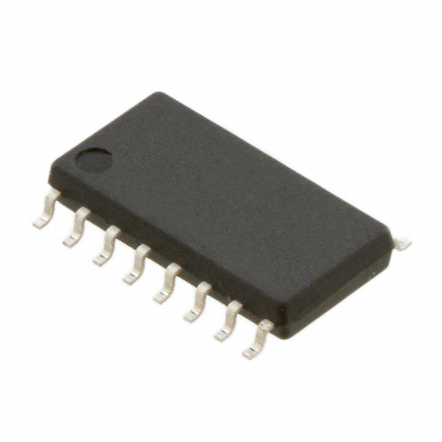
NJM3524有DIP16、DMP16、SSOP16三种封装形式。

注意事项: - 该产品将在近期停产,仅供当前使用的客户使用,并有时间限制。不适用于新项目。 - 请与地区销售办公室联系以获取更多信息。
NJM3524M-TE1 价格&库存

很抱歉,暂时无法提供与“NJM3524M-TE1”相匹配的价格&库存,您可以联系我们找货

免费人工找货