NV6113
GaNFast™ Power IC
2. Description
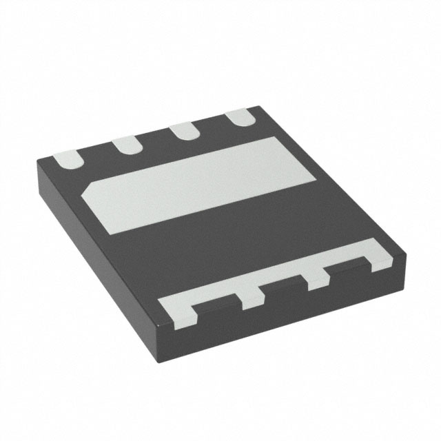
QFN 5 x 6 mm
This GaNFast power IC is optimized for high
frequency, soft-switching topologies.
Monolithic integration of FET, drive and logic creates
an easy-to-use ‘digital-in, power-out’ high-performance
powertrain building block, enabling designers to create
the fastest, smallest, most efficient power converters in
the world.
The highest dV/dt immunity, high-speed integrated
drive and industry-standard low-profile, low-inductance,
5 x 6 mm SMT QFN package allow designers to exploit
Navitas GaN technology with simple, quick, dependable
solutions for breakthrough power density and efficiency.
GaNFast power ICs extend the capabilities of
traditional topologies such as flyback, half-bridge,
resonant, etc. to MHz+ and enable the commercial
introduction of breakthrough designs.
Simplified schematic
1. Features
GaNFast™ Power IC
• Monolithically-integrated gate drive
• Wide logic input range with hysteresis
• 5 V / 15 V input-compatible
• Wide VCC range (10 to 30 V)
• Programmable turn-on dV/dt
• 200 V/ns dV/dt immunity
• 800 V Transient Voltage Rating
• 650 V Continuous Voltage rating
• Low 300 mΩ resistance
3. Topologies / Applications
•
•
•
•
•
•
•
•
•
• Zero reverse recovery charge
• ESD Protection – 2,000V (HBM), 1,000 V (CDM)
• 2 MHz operation
Small, low-profile SMT QFN
• 5 x 6 mm footprint, 0.85 mm profile
• Minimized package inductance
AC-DC, DC-DC, DC-AC
Buck, boost, half bridge, full bridge
Active Clamp Flyback, LLC resonant, Class D
Quasi-Resonant Flyback
Mobile fast-chargers, adapters
Notebook adaptors
LED lighting, solar micro-inverters
TV / monitor, wireless power
Server, telecom & networking SMPS
Environmental
• RoHS, Pb-free, REACH-compliant
4. Typical Application Circuits
DCIN(+)
DCOUT(+)
DCIN(+)
D
VCC
PWM
D
10V to 24V
PWM
Half
Bridge
Driver
IC
REG
VDD
DZ
REG
VDD
VCC
dV/dt
DZ
dV/dt
NV6113
S
D
VCC
PWM
REG
VDD
NV6113
DZ
S
dV/dt
10V to 24V
NV6113
S
DCIN(-)
DCIN(-)
DCOUT(-)
Half-bridge
Boost
Final Datasheet
PGND
1
Rev Oct 27, 2020
�NV6113
5. Table of Contents
1. Features ................................................................. 1
8.2. Normal Operating Mode .................................. 12
2. Description ............................................................ 1
8.3. Standby Mode ................................................. 12
3. Topologies / Applications ..................................... 1
8.4. Programmable Turn-on dV/dt Control .............. 12
4. Typical Application Circuits ................................. 1
8.5. Current Sensing .............................................. 13
5. Table of Contents .................................................. 2
8.6. Paralleling Devices .......................................... 13
6. Specifications ........................................................ 3
8.7. 3.3V PWM Input Circuit ................................... 14
6.1. Absolute Maximum Ratings (1) ............................ 3
8.8. PCB Layout Guidelines ................................... 14
6.2. Recommended Operating Conditions (3) ............. 3
8.9. Recommended Component Values ................. 15
6.3. ESD Ratings ...................................................... 4
8.9.1. Zener Selection ....................................... 15
6.4. Thermal Resistance ........................................... 4
8.10. Drain-to-Source Voltage Considerations........ 16
6.5. Electrical Characteristics.................................... 5
9. Recommended PCB Land Pattern ..................... 17
6.6. Switching Waveforms ........................................ 6
10. PCB Layout Guidelines .................................... 18
6.7. Characteristic Graphs ........................................ 7
11. QFN Package Outline ....................................... 20
7. Internal Schematic, Pin Configurations and
Functions ................................................................. 10
12. Tape and Reel Dimensions .............................. 21
13. Ordering Information ........................................ 22
8. Functional Description ....................................... 11
14. Revision History ............................................... 22
8.1. Start Up ........................................................... 11
Final Datasheet
2
Rev Oct 27, 2020
�NV6113
6. Specifications
6.1. Absolute Maximum Ratings(1)
(with respect to Source (pad) unless noted)
SYMBOL
PARAMETER
VDS (TRAN)
Transient Drain-to-Source Voltage
VDS (CONT)
Continuous Drain-to-Source Voltage
VCC
(2)
Supply Voltage
MAX
UNITS
800
V
-7 to +650
V
30
V
VPWM
PWM Input Pin Voltage
-3 to +30
V
VDZ
VDD Setting Pin Voltage
6.6
V
VDD
Drive Supply Voltage
7.2
V
5
A
ID
Continuous Drain Current (@ TC = 100ºC)
ID PULSE
Pulsed Drain Current (10 µs @ TJ = 25°C)
10
A
ID PULSE
Pulsed Drain Current (10 µs @ TJ = 125°C)
7.5
A
Slew Rate on Drain-to-Source
200
V/ns
Operating Junction Temperature
-55 to 150
ºC
Storage Temperature
-55 to 150
ºC
dV/dt
TJ
TSTOR
(1) Absolute maximum ratings are stress ratings; devices subjected to stresses beyond these ratings may cause permanent damage.
(2) VDS (TRAN)allows for surge ratings during non-repetitive events that are
很抱歉,暂时无法提供与“NV6113-RA”相匹配的价格&库存,您可以联系我们找货
免费人工找货