S-8241 Series
BATTERY PROTECTION IC
FOR 1-CELL PACK
www.sii-ic.com
N
Rev.9.2_00
DE
SI
G
© Seiko Instruments Inc., 1999-2013
The S-8241 Series is a series of lithium ion/lithium polymer rechargeable battery protection ICs incorporating high-accuracy
voltage detection circuits and delay circuits.
These ICs are suitable for protection of 1-cell lithium ion/lithium polymer rechargeable battery packs from overcharge,
overdischarge and overcurrent.
Features
Internal high-accuracy voltage detection circuit
• Overcharge detection voltage:
3.9 V to 4.4 V (5 mV-step)
Accuracy of ±25 mV (+25°C) and ± 30 mV (−5 to +55°C)
• Overcharge release voltage:
3.8 V to 4.4 V*1 Accuracy of ±50 mV
• Overdischarge detection voltage: 2.0 V to 3.0 V (100 mV-step) Accuracy of ±80 mV
*2
• Overdischarge release voltage:
2.0 V to 3.4 V Accuracy of ±100 mV
• Overcurrent 1 detection voltage: 0.05 V to 0.32 V (5 mV-step) Accuracy of ±20 mV
• Overcurrent 2 detection voltage: 0.5 V (fixed)
Accuracy of ±100 mV
(2) A high voltage withstand device is used for charger connection pins
(VM and CO pins: Absolute maximum rating = 26 V)
(3) Delay times (overcharge: tCU; overdischarge: tDL; overcurrent 1: tlOV1; overcurrent 2: tlOV2) are generated
by an internal circuit. (External capacitors are unnecessary.)
Accuracy of ±30%
(4) Internal three-step overcurrent detection circuit (overcurrent 1, overcurrent 2, and load short-circuiting)
(5) Either the 0 V battery charging function or 0 V battery charge inhibiting function can be selected.
(6) Products with and without a power-down function can be selected.
(7) Charger detection function and abnormal charge current detection function
• The overdischarge hysteresis is released by detecting a negative VM pin voltage (typ. −1.3 V) (Charger detection
function).
• If the output voltage at DO pin is high and the VM pin voltage becomes equal to or lower than the charger detection
voltage (typ. −1.3 V), the output voltage at CO pin goes low (Abnormal charge current detection function).
(8) Low current consumption
• Operation:
3.0 μA typ. 5.0 μA max.
• Power-down mode: 0.1 μA max.
(9) Wide operation temperature range: −40°C to +85°C
(10) Lead-free, Sn 100%, halogen-free*3
CO
MM
EN
DE
D
FO
R
NE
W
(1)
NO
T
RE
*1. Overcharge release voltage = Overcharge detection voltage - Overcharge hysteresis
The overcharge hysteresis can be selected in the range 0.0 V, or 0.1 V to 0.4 V in 50 mV steps. (However, selection
“Overcharge release voltage3.4 V” is enabled.)
*3. Refer to “ Product Name Structure” for details.
Applications
• Lithium-ion rechargeable battery pack
• Lithium- polymer rechargeable battery pack
Packages
• SOT-23-5
• SNT-6A
Seiko Instruments Inc.
1
�BATTERY PROTECTION IC FOR 1-CELL PACK
S-8241 Series
Rev.9.2_00
N
Block Diagram
DE
SI
G
Delay circuit
Clock generation circuit
VDD
Counter circuit
DO
Load shortcircuiting
detection circuit
−
Level conversion circuit
0V battery charging circuit
0V battery charge
inhibition circuit
Overdischarge
detection
comparator
RVMD
−
Overcurrent 1
detection comparator
RVMS
R
−
FO
Charger
detection circuit
The overdischarge
hysterisis is released when
a charger is detected.
DE
D
+
−
Overcurrent 2
detection comparator
Remark The diodes in the IC are parasitic diodes.
NO
T
RE
CO
MM
EN
Figure 1
2
RCOL
+
+
VSS
CO
W
Overcharge
detection
comparator
NE
+
Seiko Instruments Inc.
VM
�BATTERY PROTECTION IC FOR 1-CELL PACK
S-8241 Series
Rev.9.2_00
Product Name Structure
1. Product Name
N
S-8241A xx xx - xxx xx x
DE
SI
G
Environmental code
U:
Lead-free (Sn 100%), halogen-free
G : Lead-free (for details, please contact our sales office)
IC direction in tape specifications
T2 : SOT-23-5
TF : SNT-6A
2
*1
W
Product name (abbreviation)
NE
Package name (abbreviation)
MC : SOT-23-5
PG : SNT-6A
FO
R
Serial code
Sequentially set from BA to ZZ
*1. Refer to the tape specifications.
DE
D
*2. Refer to the “3. Product Name List”.
MM
EN
2. Package
Package name
Tape
Reel
Land
MP005-A-P-SD
PG006-A-P-SD
MP005-A-C-SD
PG006-A-C-SD
MP005-A-R-SD
PG006-A-R-SD
⎯
PG006-A-L-SD
NO
T
RE
CO
SOT-23-5
SNT-6A
Drawing code
Package
Seiko Instruments Inc.
3
�BATTERY PROTECTION IC FOR 1-CELL PACK
S-8241 Series
Rev.9.2_00
3. Product Name List
N
(1) SOT-23-5
Overcharge
detection
voltage
[VCU]
Overcharge
release
voltage
[VCL]
Overdischarge
detection
voltage
[VDL]
Overdischarge
release
voltage
[VDU]
Overcurrent 1
detection
voltage
[VIOV1]
S-8241ABAMC-GBAT2x
4.275 V
4.075 V
2.30 V
2.90 V
0.100 V
S-8241ABBMC-GBBT2x
4.280 V
3.980 V
2.30 V
2.40 V
0.125 V
S-8241ABCMC-GBCT2x
4.350 V
4.100 V
2.30 V
2.80 V
0.075 V
S-8241ABDMC-GBDT2x
4.275 V
4.175 V
2.30 V
2.40 V
0.100 V
Available
(1)
Yes
S-8241ABEMC-GBET2x
4.295 V
4.095 V
2.30 V
3.00 V
0.200 V
Unavailable
Yes
S-8241ABFMC-GBFT2x
4.325 V
4.075 V
2.50 V
2.90 V
0.100 V
Unavailable
(1)
Yes
S-8241ABGMC-GBGT2x
4.200 V
4.100 V
2.30 V
3.00 V
0.100 V
Unavailable
(1)
Yes
S-8241ABHMC-GBHT2x
4.325 V
4.125 V
2.30 V
2.30 V
NE
(1)
0.100 V
Available
(1)
Yes
S-8241ABIMC-GBIT2x
4.280 V
4.080 V
2.30 V
2.30 V
0.160 V
Unavailable
(1)
Yes
S-8241ABKMC-GBKT2x
4.325 V
4.075 V
2.50 V
2.90 V
Unavailable
(1)
Yes
S-8241ABLMC-GBLT2x
4.320 V
4.070 V
2.50 V
2.90 V
0.100 V
Unavailable
(1)
Yes
S-8241ABOMC-GBOT2x
4.350 V
4.150 V
2.30 V
3.00 V
0.150 V
Available
(2)
Yes
S-8241ABPMC-GBPT2x
4.350 V
4.150 V
2.30 V
FO
0.150 V
3.00 V
0.200 V
Available
(2)
Yes
S-8241ABQMC-GBQT2x
4.280 V
4.080 V
2.30 V
2.30 V
0.130 V
Unavailable
(1)
Yes
S-8241ABRMC-GBRT2x
4.325 V
4.075 V
2.50 V
2.90 V
0.100 V
Unavailable
(4)
Yes
S-8241ABTMC-GBTT2x
4.300 V
4.100 V
2.30 V
2.30 V
0.100 V
Available
(1)
Yes
S-8241ABUMC-GBUT2x
4.200 V
4.100 V
2.30 V
2.30 V
0.150 V
Unavailable
(1)
Yes
S-8241ABVMC-GBVT2x
4.295 V
4.095 V
DE
DE
SI
G
Table 1 (1 / 2)
2.30 V
2.30 V
0.130 V
Available
(1)
Yes
S-8241ABWMC-GBWT2x
4.280 V
4.080 V
2.30 V
2.30 V
0.130 V
Unavailable
(3)
Yes
S-8241ABXMC-GBXT2x
4.350 V
4.000 V
2.60 V
3.30 V
0.200 V
Unavailable
(1)
Yes
S-8241ABYMC-GBYT2x
4.220 V
4.220 V
2.30 V
2.30 V
0.200 V
Available
(3)
Yes
S-8241ACAMC-GCAT2x
4.280 V
4.080 V
2.30 V
2.30 V
0.200 V
Available
(1)
Yes
S-8241ACBMC-GCBT2x
4.300 V
4.100 V
2.30 V
2.30 V
0.150 V
Available
(1)
Yes
S-8241ACDMC-GCDT2x
4.275 V
4.075 V
2.30 V
2.30 V
0.100 V
Unavailable
(4)
Yes
S-8241ACEMC-GCET2x
4.295 V
4.095 V
2.30 V
0.080 V
Available
(1)
Yes
4.295 V
4.095 V
2.30 V
2.30 V
0.090 V
Available
(1)
Yes
4.295 V
4.095 V
2.30 V
2.30 V
0.060 V
Available
(1)
Yes
Delay
time
combination*1
Power down
function
Unavailable
(1)
Yes
(2)
Yes
(1)
Yes
D
R
W
Available
Unavailable
CO
MM
EN
Product Name
0 V battery
charging
function
2.30 V
4.280 V
4.080 V
2.60 V
2.60 V
0.200 V
Available
(1)
Yes
S-8241ACIMC-GCIT2x
4.350 V
4.150 V
2.05 V
2.75 V
0.200 V
Available
(2)
Yes
S-8241ACKMC-GCKT2x
4.350 V
4.150 V
2.00 V
2.00 V
0.200 V
Available
(2)
Yes
S-8241ACLMC-GCLT2x
S-8241ACFMC-GCFT2x
S-8241ACGMC-GCGT2x
RE
S-8241ACHMC-GCHT2x
4.200 V
2.50 V
3.00 V
0.100 V
Available
(1)
Yes
4.350 V
4.150 V
2.10 V
2.20 V
0.200 V
Available
(2)
Yes
S-8241ACOMC-GCOT2x
4.100 V
3.850 V
2.50 V
2.90 V
0.150 V
Unavailable
(1)
No
S-8241ACPMC-GCPT2x
4.325 V
4.075 V
2.50 V
2.90 V
0.150 V
Unavailable
(1)
No
S-8241ACQMC-GCQT2x
4.275 V
4.175 V
2.30 V
2.40 V
0.100 V
Available
(1)
No
S-8241ACRMC-GCRT2x
4.350 V
4.150 V
2.30 V
3.00 V
0.100 V
Available
(1)
No
S-8241ACSMC-GCST2x
4.180 V
3.930 V
2.50 V
2.90 V
0.150 V
Unavailable
(1)
No
S-8241ACTMC-GCTT2x
4.100 V
4.000 V
2.50 V
2.90 V
0.150 V
Unavailable
(1)
No
S-8241ACUMC-GCUT2x
4.180 V
4.080 V
2.50 V
2.90 V
0.150 V
Unavailable
(1)
No
S-8241ACXMC-GCXT2x
4.275 V
4.075 V
2.50 V
2.90 V
0.150 V
Unavailable
(1)
No
S-8241ACYMC-GCYT2x
4.275 V
4.075 V
2.60 V
2.90 V
0.100 V
Unavailable
(1)
No
NO
T
4.200 V
S-8241ACNMC-GCNT2x
4
Seiko Instruments Inc.
�BATTERY PROTECTION IC FOR 1-CELL PACK
S-8241 Series
Rev.9.2_00
S-8241ADAMC-GDAT2x
4.350 V
4.150 V
2.30 V
3.00 V
0.100 V
S-8241ADDMC-GDDT2x
4.185 V
4.085 V
2.80 V
2.90 V
0.150 V
S-8241ADEMC-GDET2x
4.350 V
4.150 V
2.10 V
2.20 V
0.150 V
S-8241ADFMC-GDFT2x
4.350 V
4.150 V
2.10 V
2.10 V
0.150 V
S-8241ADGMC-GDGT2x
S-8241ADHMC-GDHT2x
S-8241ADIMC-GDIT2x
S-8241ADJMC-GDJT2x
S-8241ADKMC-GDKT2x
S-8241ADLMC-GDLT2x
4.275 V
4.250 V
4.280 V
4.350 V
4.275 V
4.075 V
4.050 V
4.280 V
4.350 V
4.275 V
2.10 V
2.40 V
2.30 V
2.10 V
2.10 V
2.10 V
2.90 V
2.30 V
2.10 V
2.10 V
0.150 V
0.100 V
0.100 V
0.100 V
0.100 V
4.220 V
4.070 V
2.70 V
3.00 V
S-8241ADMMC-GDMT2x
4.230 V
4.080 V
2.70 V
3.00 V
S-8241ADNMC-GDNT2x
4.250 V
4.100 V
2.70 V
3.00 V
0.300 V
S-8241ADOMC-GDOT2x
4.275 V
4.175 V
2.30 V
2.40 V
S-8241ADQMC-GDQT2x
4.250 V
4.100 V
2.00 V
2.70 V
0.150 V
S-8241ADSMC-GDST2x
4.250 V
4.150 V
2.00 V
2.70 V
0.150 V
S-8241ADTMC-GDTT2x
4.180 V
4.180 V
2.50 V
S-8241ADVMC-GDVT2x
3.900 V
3.900 V
2.00 V
2.30 V
S-8241ADWMC-GDWT2x
S-8241ADXMC-GDXT2x
S-8241ADYMC-GDYT2x
S-8241ADZMC-GDZT2x
S-8241AEAMC-GEAT2x
S-8241AEBMC-GEBT2x
S-8241AECMC-GECT2x
4.100 V
4.275 V
4.000 V
4.175 V
2.50 V
2.60 V
4.100 V
4.150 V
4.180 V
4.280 V
4.000 V
4.050 V
4.080 V
4.130 V
4.100 V
4.000 V
Overdischarge
release
voltage
[VDU]
Overcurrent 1
detection
voltage
[VIOV1]
0 V battery
charging
function
Delay
time
combination*1
Power down
function
Available
(1)
Yes
Unavailable
(1)
Yes
(2)
Yes
(5)
Yes
Unavailable
Available
Unavailable
Unavailable
Unavailable
(5)
(1)
(5)
(5)
(5)
Yes
No
Yes
Yes
Yes
0.300 V
Available
(1)
Yes
0.300 V
Available
(1)
Yes
Available
(1)
Yes
0.100 V
Unavailable
(1)
No
Available
(1)
Yes
Available
(1)
Yes
3.00 V
0.100 V
Available
(1)
Yes
0.150 V
Available
(1)
Yes
2.70 V
2.70 V
0.300 V
0.100 V
Unavailable
Available
(1)
(1)
Yes
No
2.00 V
2.00 V
2.00 V
3.00 V
2.20 V
2.70 V
2.70 V
3.20 V
0.300 V
0.150 V
0.150 V
0.150 V
Unavailable
Available
Available
Unavailable
(1)
(1)
(1)
(1)
Yes
Yes
Yes
Yes
2.00 V
2.70 V
0.300 V
Unavailable
(1)
Yes
S-8241AEEMC-GEET2x
4.200 V
4.200 V
2.50 V
3.00 V
0.320 V
S-8241AEFMC-GEFT2x
4.200 V
4.100 V
2.00 V
2.70 V
0.150 V
S-8241AEHMC-GEHT2x
4.350 V
4.150 V
2.10 V
2.20 V
0.250 V
S-8241AEIMC-GEIT2x
4.350 V
4.000 V
2.40 V
3.00 V
0.270 V
S-8241AEJMC-GEJT2x
4.350 V
4.000 V
2.40 V
3.00 V
0.300 V
S-8241AEKMC-GEKT2x
4.350 V
4.000 V
2.40 V
3.00 V
0.280 V
S-8241AEMMC-GEMT2x
4.350 V
4.150 V
2.30 V
3.00 V
0.320 V
S-8241AENMC-GENT2x
4.300 V
4.100 V
2.50 V
3.00 V
0.060 V
S-8241AEOMC-GEOT2x
4.190 V
4.190 V
2.50 V
3.00 V
0.100 V
S-8241AEPMC-GEPT2x
4.215 V
4.115 V
2.80 V
3.00 V
0.100 V
S-8241AEQMC-GEQT2x
4.190 V
4.190 V
2.80 V
3.00 V
0.100 V
S-8241AETMC-GETT2x
4.220 V
4.070 V
2.70 V
3.00 V
0.200 V
S-8241AEUMC-GEUT2x
4.350 V
4.150 V
2.30 V
3.00 V
0.200 V
S-8241AEWMC-GEWT2x
4.325 V
4.075 V
2.50 V
2.90 V
0.125 V
*1. Refer to the Table 3 about the details of the delay time combinations (1) to (7).
Available
Available
Unavailable
Unavailable
Unavailable
Unavailable
Unavailable
Available
Available
Available
Available
Available
Unavailable
Unavailable
(6)
(1)
(2)
(1)
(1)
(1)
(1)
(2)
(1)
(1)
(1)
(1)
(2)
(1)
Yes
Yes
Yes
Yes
Yes
Yes
Yes
Yes
Yes
Yes
Yes
Yes
Yes
Yes
NO
T
RE
CO
MM
EN
DE
D
R
W
Available
Unavailable
NE
Overdischarge
detection
voltage
[VDL]
FO
Overcharge
release
voltage
[VCL]
DE
SI
G
Product Name
Overcharge
detection
voltage
[VCU]
N
Table 1 (2 /2)
Remark 1. Please contact our sales office for the products with detection voltage value other than those specified above.
2. x: G or U
3. Please select products of environmental code = U for Sn 100%, halogen-free products.
Seiko Instruments Inc.
5
�BATTERY PROTECTION IC FOR 1-CELL PACK
S-8241 Series
Rev.9.2_00
(2) SNT-6A
Overdischarge
detection
voltage
[VDL]
Overdischarge
release
voltage
[VDU]
Overcurrent 1
detection
voltage
[VIOV1]
4.275 V
4.280 V
4.175 V
4.080 V
2.30 V
2.30 V
2.40 V
2.30 V
0.100 V
0.160 V
4.325 V
4.350 V
4.075 V
4.150 V
2.50 V
2.30 V
2.90 V
3.00 V
0.150 V
0.200 V
4.350 V
4.350 V
4.150 V
4.000 V
2.35 V
2.60 V
2.65 V
3.30 V
4.275 V
4.295 V
4.075 V
4.095 V
2.30 V
2.30 V
2.40 V
2.30 V
S-8241ACZPG-KCZTFx
4.350 V
4.150 V
2.70 V
2.70 V
S-8241ADFPG-KDFTFx
4.350 V
4.150 V
2.10 V
2.10 V
S-8241ADHPG-KDHTFx
S-8241ADNPG-KDNTFx
S-8241ADRPG-KDRTFx
S-8241AEDPG-KEDTFx
S-8241AEGPG-KEGTFx
S-8241AENPG-KENTFx
S-8241AERPG-KERTFx
S-8241AESPG-KESTFx
S-8241AEVPG-KEVTFx
S-8241AEXPG-KEXTFU
4.250 V
4.250 V
4.280 V
4.180 V
4.000 V
4.300 V
4.300 V
4.350 V
4.350 V
4.350 V
4.050 V
4.100 V
4.080 V
3.980 V
3.900 V
4.100 V
4.100 V
4.150 V
4.100 V
4.100 V
2.40 V
2.70 V
3.00 V
2.50 V
2.35 V
2.50 V
2.40 V
2.70 V
2.30 V
2.10 V
2.90 V
3.00 V
3.20 V
2.80 V
2.65 V
3.00 V
3.00 V
2.70 V
2.80 V
2.20 V
S-8241AEYPG-KEYTFU
4.350 V
4.100 V
2.10 V
S-8241AFAPG-KFATFU
4.350 V
4.100 V
2.10 V
S-8241AFBPG-KFBTFU
4.350 V
4.100 V
2.10 V
Available
Unavailable
(1)
(1)
Yes
Yes
Unavailable
Available
(1)
(2)
Yes
Yes
0.200 V
0.200 V
Available
Unavailable
(2)
(1)
Yes
Yes
0.140 V
0.090 V
Available
(1)
Yes
Available
(1)
Yes
0.200 V
Unavailable
(2)
Yes
0.150 V
Unavailable
(5)
Yes
Available
Available
Available
Unavailable
Available
Available
Available
Available
Unavailable
No
Yes
Yes
Yes
Yes
Yes
Yes
Yes
Yes
Yes
DE
SI
G
Power down
function
Unavailable
(1)
(1)
(1)
(1)
(7)
(2)
(2)
(2)
(5)
(1)
2.20 V
0.190 V
Unavailable
(1)
Yes
2.20 V
0.200 V
Unavailable
(1)
Yes
2.20 V
0.220 V
Unavailable
(1)
Yes
FO
0.100 V
0.300 V
0.100 V
0.100 V
0.220 V
0.060 V
0.060 V
0.200 V
0.100 V
0.180 V
D
DE
MM
EN
Delay
time
combination*1
R
S-8241ACFPG-KCFTFx
0 V battery
charging
function
W
S-8241ABDPG-KBDTFx
S-8241ABIPG-KBITFx
S-8241ABKPG-KBKTFx
S-8241ABPPG-KBPTFx
S-8241ABSPG-KBSTFx
S-8241ABXPG-KBXTFx
S-8241ABZPG-KBZTFx
Overcharge
release
voltage
[VCL]
NE
Product Name
Overcharge
detection
voltage
[VCU]
N
Table 2
*1. Refer to the Table 3 about the details of the delay time combinations (1) to (7).
NO
T
RE
CO
Remark 1. Please contact our sales office for the products with detection voltage value other than those specified above.
2. x: G or U
3. Please select products of environmental code = U for Sn 100%, halogen-free products.
6
Seiko Instruments Inc.
�BATTERY PROTECTION IC FOR 1-CELL PACK
S-8241 Series
Rev.9.2_00
Table 3
Overdischarge detection
delay time
[tDL]
(1)
(2)
1.0 s
0.125 s
125 ms
31 ms
(3)
0.25 s
125 ms
(4)
2.0 s
125 ms
(5)
0.25 s
31 ms
(6)
1.0 s
125 ms
(7)
0.5 s
125 ms
Overcurrent 1 detection
delay time
[tlOV1]
N
Overcharge detection
delay time
[tCU]
DE
SI
G
Delay time
combination
8 ms
16 ms
8 ms
8 ms
16 ms
16 ms
W
8 ms
Table 4
Delay time
Symbol
NE
Remark The delay times can be changed within the range listed Table 4. For details, please contact our sales office.
Selection range
Remarks
Select a value from the left.
Select a value from the left.
Select a value from the left.
NO
T
RE
CO
MM
EN
DE
D
FO
R
Overcharge detection delay time
tCU
0.25 s
0.5 s
1.0 s
2.0 s
Overdischarge detection delay time tDL
31 ms
62.5 ms 125 ms
⎯
Overcurrent 1 detection delay time
tlOV1
4 ms
8 ms
16 ms
⎯
Remark The value surrounded by bold lines is the delay time of the standard products.
Seiko Instruments Inc.
7
�BATTERY PROTECTION IC FOR 1-CELL PACK
S-8241 Series
Rev.9.2_00
Pin Configurations
SOT-23-5
Top view
1
2
Description
Symbol
1
VM
2
VDD
Voltage detection pin between VM and VSS
(Overcurrent detection pin)
Positive power input pin
3
VSS
Negative power input pin
4
DO
5
CO
FET gate connection pin for discharge control
(CMOS output)
FET gate connection pin for charge control
(CMOS output)
3
NE
Figure 2
Pin No.
2
5
3
4
1
NO
T
RE
CO
MM
EN
Figure 3
Description
No connection
FET gate connection pin for charge control
2
CO
(CMOS output)
FET gate connection pin for discharge control
3
DO
(CMOS output)
4
VSS
Negative power input pin
5
VDD
Positive power input pin
Voltage detection pin between VM and VSS
6
VM
(Overcurrent detection pin)
*1. The NC pin is electrically open.
The NC pin can be connected to VDD or VSS.
D
6
DE
1
Symbol
NC*1
FO
Top view
R
Table 6
SNT-6A
8
N
Pin No.
DE
SI
G
4
W
5
Table 5
Seiko Instruments Inc.
�BATTERY PROTECTION IC FOR 1-CELL PACK
S-8241 Series
Rev.9.2_00
Absolute Maximum Ratings
Table 7
SOT-23-5
Power dissipation
SNT-6A
Operation ambient temperature
V
V
V
V
mW
mW
mW
°C
⎯
−40 to +125
°C
PD
⎯
Topr
NE
The absolute maximum ratings are rated values exceeding which the product could suffer physical
damage. These values must therefore not be exceeded under any conditions.
R
Caution
⎯
VSS −0.3 to VSS +12
VDD −26 to VDD +0.3
VVM −0.3 to VDD +0.3
VSS −0.3 to VDD +0.3
250 (When not mounted on board)
*1
600
*1
400
−40 to +85
VDD
VM
CO
DO
Storage temperature
Tstg
*1. When mounted on board
[Mounted board]
(1) Board size: 114.3 mm × 76.2 mm × t1.6 mm
(2) Board name: JEDEC STANDARD51-7
N
Applicable pin
DE
SI
G
Symbol
VDS
VVM
VCO
VDO
W
Item
Input voltage between VDD and VSS
VM input pin voltage
CO output pin voltage
DO output pin voltage
(Ta = 25°C unless otherwise specified)
Rating
Unit
FO
600
SOT-23-5
D
500
300
200
SNT-6A
DE
400
MM
EN
Power Disspation (PD ) [mW]
700
100
0
0
100
150
50
Ambient Temperature (Ta) [°C]
NO
T
RE
CO
Figure 4 Power Dissipation of Package (When Mounted on Board)
Seiko Instruments Inc.
9
�BATTERY PROTECTION IC FOR 1-CELL PACK
S-8241 Series
Rev.9.2_00
Electrical Characteristics
1. Other than detection delay time (25°C)
Symbol
DETECTION VOLTAGE
Overcharge detection voltage
VCU = 3.9 V to 4.4 V, 5 mV Step
VCU
Condition
⎯
Ta = -5°C to +55°C*1
When VCL ≠ VCU
When VCL = VCU
Min.
Typ.
VCU-0.025
VCU-0.030
VCL-0.050
VCL-0.025
VCU
VCU
VCL
VCL
(Ta = 25°C unless otherwise specified)
Test
Test
Max.
Unit
Condition Circuit
DE
SI
G
Item
N
Table 8
VCU+0.025
VCU+0.030
VCL+0.050
VCL+0.025
V
1
1
NO
T
RE
CO
MM
EN
DE
D
FO
R
NE
W
Overcharge release voltage
VCL
V
1
1
VCU−VCL = 0.0 V to 0.4 V, 50 mV Step
Overdischarge detection voltage
V
VDL-0.080
VDL
VDL+0.080
V
1
1
⎯
VDL = 2.0 V to 3.0 V, 100 mV Step DL
Overdischarge release voltage
VDU-0.100
VDU
VDU+0.100
When VDU ≠ VDL
V
V
1
1
VDU−VDL = 0.0 V to 0.7 V, 100 mV Step DU
When VDU = VDL
VDU-0.080
VDU
VDU+0.080
Overcurrent 1 detection voltage
V
VIOV1-0.020 VIOV1 VIOV1+0.020
V
2
1
⎯
VIOV1 = 0.05 V to 0.32 V, 5 mV Step IOV1
Overcurrent 2 detection voltage
VIOV2
0.4
0.5
0.6
V
2
1
⎯
Load short-circuiting detection
VSHORT VM voltage based on VDD
-1.7
-1.3
-0.9
V
2
1
voltage
Charger detection voltage
VCHA
-2.0
-1.3
-0.6
V
3
1
⎯
Overcharge detection voltage
TCOE1 Ta = -5°C to +55°C
-0.5
0
0.5
mV/°C
⎯
⎯
temperature factor *1
Overcurrent 1 detection voltage
TCOE2 Ta = -5°C to +55°C
-0.1
0
0.1
mV/°C
⎯
⎯
*1
temperature factor
INPUT VOLTAGE, OPERATING VOLTAGE
Input voltage between VDD and
VDS1
absolute maximum rating
-0.3
12
V
⎯
⎯
⎯
VSS
Input voltage between VDD and VM VDS2
absolute maximum rating
-0.3
26
V
⎯
⎯
⎯
Operating voltage between VDD
VDSOP1 Internal circuit operating voltage
1.5
8
V
⎯
⎯
⎯
and VSS
Operating voltage between VDD
24
VDSOP2 Internal circuit operating voltage
1.5
V
⎯
⎯
⎯
and VM
CURRENT CONSUMPTION Power-down function available
Current consumption during normal
IOPE
VDD = 3.5 V, VVM = 0 V
1.0
3.0
5.0
4
1
μA
operation
Current consumption at power
IPDN
VDD = VVM = 1.5 V
0.1
4
1
⎯
⎯
μA
down
CURRENT CONSUMPTION Power-down function unavailable
Current consumption during normal
IOPE
VDD = 3.5 V, VVM = 0 V
1.0
3.0
5.0
4
1
μA
operation
Overdischarge current
IOPED
VDD = VVM = 1.5 V
1.0
2.0
3.5
4
1
μA
consumption
OUTPUT RESISTANCE
CO pin H resistance
RCOH VCO = 3.0 V, VDD = 3.5 V, VVM = 0 V
0.1
2
10
6
1
kΩ
CO pin L resistance
RCOL VCO = 0.5 V, VDD = 4.5 V, VVM = 0 V
150
600
2400
6
1
kΩ
DO pin H resistance
RDOH VDO = 3.0 V, VDD = 3.5 V, VVM = 0 V
0.1
1.3
6.0
7
1
kΩ
DO pin L resistance
RDOL
VDO = 0.5 V, VDD = VVM = 1.8 V
0.1
0.5
2.0
7
1
kΩ
VM INTERNAL RESISTANCE
Internal resistance between VM
RVMD
VDD = 1.8 V, VVM = 0 V
100
300
900
5
1
kΩ
and VDD
Internal resistance between VM
RVMS
VDD = VVM = 3.5 V
50
100
150
5
1
kΩ
and VSS
0 V BATTERY CHARGING FUNCTION The 0 V battery function is either "0 V battery charging function" or "0 V battery charge inhibiting function"
depending upon the product type.
0 V battery charge starting charger
V0CHA 0 V battery charging Available
0.0
0.8
1.5
V
10
1
voltage
0 V battery charge inhibiting
V0INH
0 V battery charging Unavailable
0.6
0.9
1.2
V
11
1
battery voltage
*1. Since products are not screened at high and low temperatures, the specification for this temperature range is guaranteed by design, not tested in
production.
10
Seiko Instruments Inc.
�BATTERY PROTECTION IC FOR 1-CELL PACK
S-8241 Series
Rev.9.2_00
2. Other than detection delay time (-40°C to +85°C*1)
Table 9
N
Symbol
Condition
DE
SI
G
Item
(Ta = -40°C to +85°C*1 unless otherwise specified)
Test
Test
Min.
Typ.
Max.
Unit
Condition Circuit
NO
T
RE
CO
MM
EN
DE
D
FO
R
NE
W
DETECTION VOLTAGE
Overcharge detection voltage
VCU
VCU-0.055
VCU
VCU+0.040
V
1
1
⎯
VCU = 3.9 V to 4.4 V, 5 mV Step
Overcharge release voltage
VCL-0.095
VCL
VCL+0.060
When VCL ≠ VCU
VCL
V
1
1
VCU −VCL = 0.0 V to 0.4 V, 50 mV Step
When VCL = VCU
VCL-0.055
VCL
VCL+0.040
Overdischarge detection voltage
VDL
VDL-0.120
VDL
VDL+0.120
V
1
1
⎯
VDL = 2.0 V to 3.0 V, 100 mV Step
Overdischarge release voltage
VDU-0.140
VDU
VDU+0.140
When VDU ≠ VDL
VDU
V
1
1
VDU−VDL = 0.0 V to 0.7 V, 100 mV Step
When VDU = VDL
VDU-0.120
VDU
VDU+0.120
Overcurrent 1 detection voltage
V
VIOV1-0.026 VIOV1 VIOV1+0.026
V
2
1
⎯
VIOV1 = 0.05 V to 0.32 V, 5 mV Step IOV1
Overcurrent 2 detection voltage
VIOV2
0.37
0.5
0.63
V
2
1
⎯
Load short-circuiting detection
VSHORT VM voltage based on VDD
-1.9
-1.3
-0.7
V
2
1
voltage
Charger detection voltage
VCHA
-2.2
-1.3
-0.4
V
3
1
⎯
Overcharge detection voltage
TCOE1 Ta = -40°C to +85°C
-0.7
0
0.7
mV/°C
⎯
⎯
*1
temperature factor
Overcurrent 1 detection voltage
TCOE2 Ta = -40°C to +85°C
-0.2
0
0.2
mV/°C
⎯
⎯
temperature factor *1
INPUT VOLTAGE, OPERATING VOLTAGE
Input voltage between VDD and
VDS1
absolute maximum rating
-0.3
12
V
⎯
⎯
⎯
VSS
26
Input voltage between VDD and VM VDS2
absolute maximum rating
-0.3
V
⎯
⎯
⎯
Operating voltage between VDD
VDSOP1 Internal circuit operating voltage
1.5
8
V
⎯
⎯
⎯
and VSS
Operating voltage between VDD
VDSOP2 Internal circuit operating voltage
1.5
24
V
⎯
⎯
⎯
and VM
CURRENT CONSUMPTION Power-down function available
Current consumption during normal
4
1
IOPE
VDD = 3.5 V, VVM = 0 V
0.7
3.0
6.0
μA
operation
0.1
4
1
Current consumption at power down IPDN
VDD = VVM = 1.5 V
⎯
⎯
μA
CURRENT CONSUMPTION Power-down function unavailable
Current consumption during normal
IOPE
VDD = 3.5 V, VVM = 0 V
0.7
3.0
6.0
4
1
μA
operation
4
1
Overdischarge current consumption IOPED VDD = VVM = 1.5 V
0.6
2.0
4.5
μA
OUTPUT RESISTANCE
CO pin H resistance
RCOH VCO = 3.0 V, VDD = 3.5 V, VVM = 0 V
0.07
2
13
6
1
kΩ
CO pin L resistance
RCOL VCO = 0.5 V, VDD = 4.5 V, VVM = 0 V
100
600
3500
6
1
kΩ
7
1
DO pin H resistance
RDOH VDO = 3.0 V, VDD = 3.5 V, VVM = 0 V
0.07
1.3
7.3
kΩ
DO pin L resistance
RDOL VDO = 0.5 V, VDD = VVM = 1.8 V
0.07
0.5
2.5
7
1
kΩ
VM INTERNAL RESISTANCE
Internal resistance between VM and
5
1
RVMD VDD = 1.8 V, VVM = 0 V
78
300
1310
kΩ
VDD
Internal resistance between VM and
RVMS VDD = VVM = 3.5 V
39
100
220
5
1
kΩ
VSS
0 V BATTERY CHARGING FUNCTION The 0 V battery function is either "0 V battery charging function" or "0 V battery charge inhibiting function"
depending upon the product type.
0 V battery charge starting charger
V0CHA 0 V battery charging Available
0.0
0.8
1.7
V
10
1
voltage
0 V battery charge inhibiting
V0INH 0 V battery charging Unavailable
0.4
0.9
1.4
V
11
1
battery voltage
*1. Since products are not screened at high and low temperatures, the specification for this temperature range is guaranteed by design, not tested in
production.
Seiko Instruments Inc.
11
�BATTERY PROTECTION IC FOR 1-CELL PACK
S-8241 Series
Rev.9.2_00
3. Detection delay time
DE
SI
G
N
(1) S-8241ABA, S-8241ABC, S-8241ABD, S-8241ABE, S-8241ABF, S-8241ABG, S-8241ABH,
S-8241ABI, S-8241ABK, S-8241ABL, S-8241ABQ, S-8241ABT, S-8241ABU, S-8241ABV,
S-8241ABX, S-8241ABZ, S-8241ACA, S-8241ACB, S-8241ACE, S-8241ACF, S-8241ACG,
S-8241ACH, S-8241ACL, S-8241ACO, S-8241ACP, S-8241ACQ, S-8241ACR, S-8241ACS,
S-8241ACT, S-8241ACU, S-8241ACX, S-8241ACY, S-8241ADA, S-8241ADD, S-8241ADH,
S-8241ADL, S-8241ADM, S-8241ADN, S-8241ADO, S-8241ADQ, S-8241ADR, S-8241ADS,
S-8241ADT, S-8241ADV, S-8241ADW, S-8241ADX, S-8241ADY, S-8241ADZ, S-8241AEA,
S-8241AEB, S-8241AEC, S-8241AED, S-8241AEF, S-8241AEI, S-8241AEJ, S-8241AEK,
S-8241AEM, S-8241AEO, S-8241AEP, S-8241AEQ, S-8241AET, S-8241AEW, S-8241AEX,
S-8241AEY, S-8241AFA, S-8241AFB
DELAY TIME (Ta = 25°C)
Overcharge detection delay time
Condition
tCU
⎯
Overdischarge detection delay time
tDL
⎯
Overcurrent 1 detection delay time
tlOV1
⎯
Overcurrent 2 detection delay time
tlOV2
⎯
Load short-circuiting detection delay time
tSHORT
Overdischarge detection delay time
tDL
Overcurrent 1 detection delay time
tIOV1
Overcurrent 2 detection delay time
tIOV2
Load short-circuiting detection delay time
tSHORT
Max.
Unit
Test
Test
Condition Circuit
0.7
1.0
1.3
s
8
1
125
162.5
ms
8
1
5.6
8
10.4
ms
9
1
1.4
2
2.6
ms
9
1
⎯
⎯
10
50
μs
9
1
⎯
0.55
1.0
1.7
s
8
1
⎯
69
125
212
ms
8
1
⎯
4.4
8
14
ms
9
1
⎯
1.1
2
3.4
ms
9
1
9
1
FO
DE
tCU
Typ.
87.5
D
DELAY TIME (Ta = −40°C to +85°C) *1
Overcharge detection delay time
Min.
NE
Symbol
R
Item
W
Table 10
⎯
⎯
10
73
μs
MM
EN
*1. Since products are not screened at high and low temperature, the specification for this temperature range is guaranteed by
design, not tested in production.
Table 11
Symbol
Condition
Min.
Typ.
Max.
Unit
Item
CO
(2) S-8241ABB, S-8241ABO, S-8241ABP, S-8241ABS, S-8241ACI, S-8241ACK, S-8241ACN,
S-8241ACZ, S-8241ADE, S-8241AEH, S-8241AEN, S-8241AER, S-8241AES, S-8241AEU
RE
DELAY TIME (Ta = 25°C)
Overcharge detection delay time
Test
Test
Condition Circuit
⎯
87.5
125
162.5
ms
8
1
tDL
⎯
21
31
41
ms
8
1
Overcurrent 1 detection delay time
tlOV1
⎯
11
16
21
ms
9
1
tlOV2
⎯
1.4
2
2.6
ms
9
1
tSHORT
⎯
⎯
10
50
μs
9
1
Overcharge detection delay time
tCU
⎯
69
125
212
ms
8
1
Overdischarge detection delay time
tDL
⎯
17
31
53
ms
8
1
Overcurrent 1 detection delay time
tIOV1
⎯
9
16
27
ms
9
1
Overcurrent 2 detection delay time
tIOV2
⎯
1.1
2
3.4
ms
9
1
Load short-circuiting detection delay time
tSHORT
⎯
⎯
10
73
μs
9
1
NO
T
tCU
Overdischarge detection delay time
Overcurrent 2 detection delay time
Load short-circuiting detection delay time
DELAY TIME (Ta = −40°C to +85°C)
*1
*1. Since products are not screened at high and low temperature, the specification for this temperature range is guaranteed by
design, not tested in production.
12
Seiko Instruments Inc.
�BATTERY PROTECTION IC FOR 1-CELL PACK
S-8241 Series
Rev.9.2_00
(3) S-8241ABW, S-8241ABY
Min.
Typ.
tCU
⎯
0.175
0.25
0.325
s
8
1
Overdischarge detection delay time
tDL
⎯
87.5
125
162.5
ms
8
1
Overcurrent 1 detection delay time
tlOV1
⎯
5.6
8
10.4
ms
9
1
Overcurrent 2 detection delay time
tlOV2
⎯
1.4
2
2.6
ms
9
1
tSHORT
⎯
⎯
10
50
μs
9
1
Overcharge detection delay time
tCU
⎯
0.138
0.25
0.425
s
8
1
Overdischarge detection delay time
tDL
⎯
69
125
212
ms
8
1
Overcurrent 1 detection delay time
tIOV1
⎯
8
14
ms
9
1
Overcurrent 2 detection delay time
tIOV2
⎯
1.1
2
3.4
ms
9
1
Load short-circuiting detection delay time
tSHORT
⎯
⎯
10
73
μs
9
1
DELAY TIME (Ta = 25°C)
Overcharge detection delay time
Load short-circuiting detection delay time
NE
4.4
R
DELAY TIME (Ta = −40°C to +85°C)
*1
Max.
Unit
Test
Test
Condition Circuit
Condition
DE
SI
G
Symbol
W
Item
N
Table 12
FO
*1. Since products are not screened at high and low temperature, the specification for this temperature range is guaranteed by
design, not tested in production.
D
(4) S-8241ABR, S-8241ACD
Symbol
Test
Test
Condition Circuit
Condition
Min.
Typ.
Max.
Unit
tCU
⎯
1.4
2.0
2.6
s
8
1
Overdischarge detection delay time
tDL
⎯
87.5
125
162.5
ms
8
1
Overcurrent 1 detection delay time
tlOV1
⎯
5.6
9
1
DELAY TIME (Ta = 25°C)
Overcharge detection delay time
MM
EN
Item
DE
Table 13
8
10.4
ms
tlOV2
⎯
1.4
2
2.6
ms
9
1
tSHORT
⎯
⎯
10
50
μs
9
1
tCU
⎯
1.1
2.0
3.4
s
8
1
Overdischarge detection delay time
tDL
⎯
69
125
212
ms
8
1
Overcurrent 1 detection delay time
tIOV1
⎯
4.4
8
14
ms
9
1
Overcurrent 2 detection delay time
tIOV2
⎯
1.1
2
3.4
ms
9
1
Load short-circuiting detection delay time
tSHORT
⎯
⎯
10
73
μs
9
1
Overcurrent 2 detection delay time
Load short-circuiting detection delay time
DELAY TIME (Ta = −40°C to +85°C)
RE
CO
Overcharge detection delay time
*1
NO
T
*1. Since products are not screened at high and low temperature, the specification for this temperature range is guaranteed by
design, not tested in production.
Seiko Instruments Inc.
13
�BATTERY PROTECTION IC FOR 1-CELL PACK
S-8241 Series
Rev.9.2_00
Table 14
Symbol
Condition
Min.
Typ.
Max.
Unit
Test
Test
Condition Circuit
DE
SI
G
Item
N
(5) S-8241ADF, S-8241ADG, S-8241ADI, S-8241ADJ, S-8241ADK, S-8241AEV
FO
R
NE
W
DELAY TIME (Ta = 25°C)
Overcharge detection delay time
tCU
⎯
0.175 0.25 0.325
ms
8
1
Overdischarge detection delay time
tDL
⎯
21
31
41
ms
8
1
Overcurrent 1 detection delay time
tlOV1
⎯
11
16
21
ms
9
1
Overcurrent 2 detection delay time
tlOV2
⎯
1.4
2
2.6
ms
9
1
Load short-circuiting detection delay time tSHORT
⎯
⎯
10
50
μs
9
1
DELAY TIME (Ta = −40°C to +85°C) *1
Overcharge detection delay time
tCU
⎯
0.138
0.25 0.425
s
8
1
Overdischarge detection delay time
tDL
⎯
17
31
53
ms
8
1
Overcurrent 1 detection delay time
tIOV1
⎯
9
16
27
ms
9
1
Overcurrent 2 detection delay time
tIOV2
⎯
1.1
2
3.4
ms
9
1
Load short-circuiting detection delay time tSHORT
⎯
⎯
10
73
μs
9
1
*1. Since products are not screened at high and low temperature, the specification for this temperature range is guaranteed by
design, not tested in production.
(6) S-8241AEE
Symbol
DELAY TIME (Ta = 25°C)
Overcharge detection delay time
Typ.
Max.
Unit
Test
Test
Condition Circuit
0.7
1.0
1.3
s
8
1
⎯
87.5
125
162.5
ms
8
1
⎯
11
16
21
ms
9
1
⎯
1.4
2
2.6
ms
9
1
tSHORT
⎯
⎯
10
50
μs
9
1
Overcurrent 1 detection delay time
tlOV1
tlOV2
MM
EN
tDL
Load short-circuiting detection delay time
Min.
⎯
tCU
Overdischarge detection delay time
Overcurrent 2 detection delay time
Condition
DE
Item
D
Table 15
DELAY TIME (Ta = −40°C to +85°C) *1
Overcharge detection delay time
Overdischarge detection delay time
⎯
0.55
1.0
1.7
s
8
1
⎯
69
125
212
ms
8
1
tIOV1
⎯
9
16
27
ms
9
1
tIOV2
⎯
1.1
2
3.4
ms
9
1
tSHORT
⎯
9
1
CO
Overcurrent 1 detection delay time
tCU
tDL
Overcurrent 2 detection delay time
Load short-circuiting detection delay time
⎯
10
73
μs
NO
T
RE
*1. Since products are not screened at high and low temperature, the specification for this temperature range is guaranteed by
design, not tested in production.
14
Seiko Instruments Inc.
�BATTERY PROTECTION IC FOR 1-CELL PACK
S-8241 Series
Rev.9.2_00
(7) S-8241AEG
Table 16
DELAY TIME (Ta = 25°C)
Overcharge detection delay time
Condition
Min.
Typ.
Max.
Test
Test
Condition Circuit
N
Symbol
Unit
DE
SI
G
Item
tCU
⎯
0.35
0.5
0.65
s
8
1
Overdischarge detection delay time
tDL
⎯
87.5
125
162.5
ms
8
1
Overcurrent 1 detection delay time
tlOV1
⎯
5.6
8
10.4
ms
9
1
Overcurrent 2 detection delay time
tlOV2
⎯
1.4
2
2.6
ms
9
1
Load short-circuiting detection delay time
tSHORT
⎯
⎯
10
50
μs
9
1
Overcharge detection delay time
tCU
⎯
0.275
0.5
0.85
s
8
1
Overdischarge detection delay time
tDL
⎯
69
125
ms
8
1
Overcurrent 1 detection delay time
tIOV1
⎯
4.4
1
Overcurrent 2 detection delay time
tIOV2
⎯
tSHORT
⎯
212
8
14
ms
9
2
3.4
ms
9
1
9
1
NE
Load short-circuiting detection delay time
W
DELAY TIME (Ta = −40°C to +85°C) *1
1.1
⎯
10
73
μs
NO
T
RE
CO
MM
EN
DE
D
FO
R
*1. Since products are not screened at high and low temperature, the specification for this temperature range is guaranteed by
design, not tested in production.
Seiko Instruments Inc.
15
�BATTERY PROTECTION IC FOR 1-CELL PACK
S-8241 Series
Rev.9.2_00
Test Circuits
Unless otherwise specified, the output voltage levels “H” and “L” at CO pin (VCO) and DO pin (VDO) are
judged by the threshold voltage (1.0 V) of the N-channel FET. Judge the CO pin level with respect to VVM
and the DO pin level with respect to VSS.
DE
SI
G
N
Caution
(1) Test Condition 1, Test Circuit 1
(Overcharge detection voltage, Overcharge release voltage, Overdischarge detection voltage, Overdischarge
release voltage)
W
The overcharge detection voltage (VCU) is defined by the voltage between VDD and VSS at which VCO goes “L” from “H”
when the voltage V1 is gradually increased from the normal condition V1 = 3.5 V and V2 = 0 V. The overcharge release
voltage (VCL) is defined by the voltage between VDD and VSS at which VCO goes “H” from “L” when the voltage V1 is
then gradually decreased.
NE
Gradually decreasing the voltage V1, the overdischarge detection voltage (VDL) is defined by the voltage between VDD
and VSS at which VDO goes “L” from “H”. The overdischarge release voltage (VDU) is defined by the voltage between
VDD and VSS at which VDO goes “H” from “L” when the voltage V1 is then gradually increased.
R
(2) Test Condition 2, Test Circuit 1
(Overcurrent 1 detection voltage, Overcurrent 2 detection voltage, Load short-circuiting detection voltage)
DE
D
FO
The overcurrent 1 detection voltage (VIOV1) is defined by the voltage between VDD and VSS at which VDO goes “L” from
“H” when the voltage V2 is gradually increased from the normal condition V1 = 3.5 V and V2 = 0 V.
The overcurrent 2 detection voltage (VIOV2) is defined by the voltage between VDD and VSS at which VDO goes “L” from
“H” when the voltage V2 is increased at the speed between 1 ms and 4 ms from the normal condition V1 = 3.5 V and V2
= 0 V.
The load short-circuiting detection voltage (VSHORT) is defined by the voltage between VDD and VSS at which VDO goes
“L” from “H” when the voltage V2 is increased at the speed between 1 μs and 50 μs from the normal condition V1 = 3.5
V and V2 = 0 V.
MM
EN
(3) Test Condition 3, Test Circuit 1
(Charger detection voltage, ( = abnormal charge current detection voltage) )
CO
• Applied only for products with overdischarge hysteresis
Set V1 = 1.8 V and V2 = 0 V under overdischarge condition. Increase V1 gradually, set V1 = (VDU+VDL) / 2 (within
overdischarge hysteresis, overdischarge condition), then decrease V2 from 0 V gradually. The voltage between VM
and VSS at which VDO goes “H” from “L” is the charger detection voltage (VCHA).
• Applied only for products without overdischarge hysteresis
Set V1 = 3.5 V and V2 = 0 V under normal condition. Decrease V2 from 0 V gradually. The voltage between VM and
VSS at which VCO goes “L” from “H” is the abnormal charge current detection voltage. The abnormal charge current
detection voltage has the same value as the charger detection voltage (VCHA).
RE
(4) Test Condition 4, Test Circuit 1
(Normal operation current consumption, Power-down current consumption, Overdischarge current
consumption)
NO
T
Set V1 = 3.5 V and V2 = 0 V under normal condition. The current IDD flowing through VDD pin is the normal operation
consumption current (IOPE).
• For products with power-down function
Set V1 = V2 = 1.5 V under overdischarge condition. The current IDD flowing through VDD pin is the power-down
current consumption (IPDN).
• For products without power-down function
Set V1 = V2 = 1.5 V under overdischarge condition. The current IDD flowing through VDD pin is the overdischarge
current consumption (IOPED).
16
Seiko Instruments Inc.
�BATTERY PROTECTION IC FOR 1-CELL PACK
S-8241 Series
Rev.9.2_00
(5) Test Condition 5, Test Circuit 1
(Internal resistance between VM and VDD, Internal resistance between VM and VSS)
DE
SI
G
N
Set V1 = 1.8 V and V2 = 0 V under overdischarge condition. Measure current IVM flowing through VM pin. 1.8V / |IVM|
gives the internal resistance (RVMD) between VM and VDD.
Set V1 = V2 = 3.5 V under overcurrent condition. Measure current IVM flowing through VM pin. 3.5 V / |IVM| gives the
internal resistance (RVMS) between VM and VSS.
(6) Test Condition 6, Test Circuit 1
(CO pin H resistance, CO pin L resistance)
W
Set V1 = 3.5 V, V2 = 0 V and V3 = 3.0 V under normal condition. Measure current ICO flowing through CO pin. 0.5 V /
|ICO| is the CO pin H resistance (RCOH).
Set V1 = 4.5 V, V2 = 0 V and V3 = 0.5 V under overcharge condition. Measure current ICO flowing through CO pin. 0.5
V / |ICO| is the CO pin L resistance (RCOL).
NE
(7) Test Condition 7, Test Circuit 1
(DO pin H resistance, DO pin L resistance)
FO
R
Set V1 = 3.5 V, V2 = 0 V and V4 = 3.0 V under normal condition. Measure current IDO flowing through DO pin. 0.5 V /
|IDO| gives the DO pin H resistance (RDOH).
Set V1 = 1.8 V, V2 = 0 V and V4 = 0.5 V under overdischarge condition. Measure current IDO flowing through DO pin.
0.5 V / |IDO| gives the DO pin L resistance (RDOL).
(8) Test Condition 8, Test Circuit 1
(Overcharge detection delay time, Overdischarge detection delay time)
MM
EN
DE
D
Set V1 = 3.5 V and V2 = 0 V under normal condition. Increase V1 gradually to overcharge detection voltage VCU - 0.2 V
and increase V1 to the overcharge detection voltage VCU + 0.2 V momentarily (within 10 μs). The time after V1 becomes
the overcharge detection voltage until VCO goes "L" is the overcharge detection delay time (tCU).
Set V1 = 3.5 V and V2 = 0 V under normal condition. Decrease V1 gradually to overdischarge detection voltage VDL +
0.2 V and decrease V1 to the overdischarge detection voltage VDL - 0.2 V momentarily (within 10 μs). The time after V1
becomes the overdischarge detection voltage VDL until VDO goes "L" is the overdischarge detection delay time (tDL).
(9) Test Condition 9, Test Circuit 1
(Overcurrent 1 detection delay time, Overcurrent 2 detection delay time, Load short-circuiting detection delay
time, Abnormal charge current detection delay time)
Caution
RE
CO
Set V1 = 3.5 V and V2 = 0 V under normal condition. Increase V2 from 0 V to 0.35 V momentarily (within 10 μs). The
time after V2 becomes overcurrent 1 detection voltage (VIOV1) until VDO goes "L" is overcurrent 1 detection delay time
(tIOV1).
Set V1 = 3.5 V and V2 = 0 V under normal condition. Increase V2 from 0 V to 0.7 V momentarily (within 1 μs). The time
after V2 becomes overcurrent 1 detection voltage (VIOV1) until VDO goes "L" is overcurrent 2 detection delay time (tIOV2).
The overcurrent 2 detection delay time starts when the overcurrent 1 is detected, since the delay
circuit is common.
NO
T
Set V1 = 3.5 V and V2 = 0 V under normal condition. Increase V2 from 0 V to 3.0 V momentarily (within 1 μs). The time
after V2 becomes the load short-circuiting detection voltage (VSHORT) until VDO goes "L" is the load short-circuiting
detection delay time (tSHORT).
Set V1 = 3.5 V and V2 = 0 V under normal condition. Decrease V2 from 0 V to -2.5 V momentarily (within 10 μs). The
time after V2 becomes the charger detection voltage (VCHA) until VCO goes "L" is the abnormal charge current detection
delay time. The abnormal charge current detection delay time has the same value as the overcharge detection delay
time.
Seiko Instruments Inc.
17
�BATTERY PROTECTION IC FOR 1-CELL PACK
S-8241 Series
Rev.9.2_00
(10) Test Condition 10, Test Circuit 1 (Product with 0 V battery charging function)
(0 V battery charge start charger voltage)
DE
SI
G
N
Set V1 = V2 = 0 V and decrease V2 gradually. The voltage between VDD and VM at which VCO goes “H” (VVM + 0.1 V
or higher) is the 0 V battery charge starting charger voltage (V0CHA).
(11) Test Condition 11, Test Circuit 1 (Product with 0 V battery charge inhibiting function)
(0 V battery charge inhibiting battery voltage)
Set V1 = 0 V and V2 = -4 V. Increase V1 gradually. The voltage between VDD and VSS at which VCO goes “H” (VVM +
0.1 V or higher) is the 0 V battery charge inhibiting battery voltage (V0INH).
IDD
NE
S-8241 Series
V1
W
VDD
A
VM
CO
DO
IDO
A
VCO
V
Test circuit 1
DE
COM
V VDO
D
V4
FO
R
VSS
NO
T
RE
CO
MM
EN
Figure 5
18
Seiko Instruments Inc.
A ICO
V3
A IVM
V2
�BATTERY PROTECTION IC FOR 1-CELL PACK
S-8241 Series
Rev.9.2_00
Operation
Remark Refer to the “ Battery Protection IC Connection Example”.
N
1. Normal Status
DE
SI
G
The S-8241 monitors the voltage of the battery connected to VDD and VSS pins and the voltage difference between VM
and VSS pins to control charging and discharging. When the battery voltage is in the range from the overdischarge
detection voltage (VDL) to the overcharge detection voltage (VCU), and the VM pin voltage is in the range from the
charger detection voltage (VCHA) to the overcurrent 1 detection voltage (VIOV1) (the current flowing through the battery is
equal to or lower than a specified value), the IC turns both the charging and discharging control FETs on. This status is
called normal status and in this status charging and discharging can be carried out freely.
W
2. Overcurrent Status
D
FO
R
NE
When the discharging current becomes equal to or higher than a specified value (the VM pin voltage is equal to or higher
than the overcurrent detection voltage) during discharging under normal status and the state continues for the
overcurrent detection delay time or longer, the S-8241 turns the discharging control FET off to stop discharging. This
status is called overcurrent status. (The overcurrent includes overcurrent 1, overcurrent 2, or load short-circuiting.)
The VM and VSS pins are shorted internally by the RVMS resistor under the overcurrent status. When a load is
connected, the VM pin voltage equals the VDD voltage due to the load.
The overcurrent status returns to the normal status when the load is released and the impedance between the EB+ and
EB- pins (see the Figure 12 for a connection example) becomes higher than the automatic recoverable impedance (see
the equation [1] below). When the load is removed, the VM pin goes back to the VSS potential since the VM pin is
shorted the VSS pin with the RVMS resistor. Detecting that the VM pin potential is lower than the overcurrent 1 detection
voltage (VIOV1), the IC returns to the normal status.
DE
Automatic recoverable impedance = {Battery voltage / (Minimum value of overcurrent 1 detection voltage) − 1} x (RVMS
maximum value) --- [1]
MM
EN
Example: Battery voltage = 3.5 V and overcurrent 1 detection voltage (VIOV1) = 0.1 V
Automatic recoverable impedance = (3.5 V / 0.07 V −1) x 200 kΩ = 9.8 MΩ
NO
T
RE
CO
Remark The automatic recoverable impedance varies with the battery voltage and overcurrent 1 detection voltage
settings. Determine the minimum value of the open load using the above equation [1] to have automatic
recovery from the overcurrent status work after checking the overcurrent 1 detection voltage setting for the IC.
Seiko Instruments Inc.
19
�BATTERY PROTECTION IC FOR 1-CELL PACK
S-8241 Series
Rev.9.2_00
3. Overcharge Status
DE
SI
G
N
When the battery voltage becomes higher than the overcharge detection voltage (VCU) during charging under normal
status and the state continues for the overcharge detection delay time (tCU) or longer, the S-8241 turns the charging
control FET off to stop charging. This status is called the overcharge status.
The overcharge status is released in the following two cases ((1) and (2)) depending on the products with and without
overcharge hysteresis:
FO
R
NE
W
Products with overcharge hysteresis (overcharge detection voltage (VCU) > overcharge release voltage (VCL))
(1) When the battery voltage drops below the overcharge release voltage (VCL), the S-8241 turns the charging control
FET on and returns to the normal status.
(2) When a load is connected and discharging starts, the S-8241 turns the charging control FET on and returns to the
normal status. The release mechanism is as follows: the discharging current flows through an internal parasitic
diode of the charging FET immediately after a load is connected and discharging starts, and the VM pin voltage
increases about 0.7 V (Vf voltage of the diode) from the VSS pin voltage momentarily. The IC detects this voltage
(being higher than the overcurrent 1 detection voltage) and releases the overcharge status. Consequently, in the
case that the battery voltage is equal to or lower than the overcharge detection voltage (VCU), the IC returns to the
normal status immediately, but in the case the battery voltage is higher than the overcharge detection voltage (VCU),
the IC does not return to the normal status until the battery voltage drops below the overcharge detection voltage
(VCU) even if the load is connected. In addition if the VM pin voltage is equal to or lower than the overcurrent 1
detection voltage when a load is connected and discharging starts, the IC does not return to the normal status.
DE
D
Remark If the battery is charged to a voltage higher than the overcharge detection voltage (VCU) and the battery
voltage does not drop below the overcharge detection voltage (VCU) even when a heavy load, which
causes an overcurrent, is connected, the overcurrent 1 and overcurrent 2 do not work until the battery
voltage drops below the overcharge detection voltage (VCU). Since an actual battery has, however, an
internal impedance of several dozens of mΩ, and the battery voltage drops immediately after a heavy load
which causes an overcurrent is connected, the overcurrent 1 and overcurrent 2 work. Detection of load
short-circuiting works regardless of the battery voltage.
RE
CO
MM
EN
Products without overcharge hysteresis (Overcharge detection voltage (VCU) = Overcharge release voltage (VCL))
(1) When the battery voltage drops below the overcharge release voltage (VCL), the S-8241 turn the charging control
FET on and returns to the normal status.
(2) When a load is connected and discharging starts, the S-8241 turns the charging control FET on and returns to the
normal status. The release mechanism is explained as follows : the discharging current flows through an internal
parasitic diode of the charging FET immediately after a load is connected and discharging starts, and the VM pin
voltage increases about 0.7 V (Vf voltage of the diode) from the VSS pin voltage momentarily. Detecting this voltage
(being higher than the overcurrent 1 detection voltage), the IC increases the overcharge detection voltage about 50
mV, and releases the overcharge status. Consequently, when the battery voltage is equal to or lower than the
overcharge detection voltage (VCU) + 50 mV, the S-8241 immediately returns to the normal status. But the battery
voltage is higher than the overcharge detection voltage (VCU) + 50 mV, the S-8241 does not return to the normal
status until the battery voltage drops below the overcharge detection voltage (VCU) + 50 mV even if a load is
connected. If the VM pin voltage is equal to or lower than the overcurrent 1 detection voltage when a load is
connected and discharging starts, the S-8241 does not return to the normal status.
NO
T
Remark If the battery is charged to a voltage higher than the overcharge detection voltage (VCU) and the battery
voltage does not drop below the overcharge detection voltage (VCU) + 50 mV even when a heavy load,
which causes an overcurrent, is connected, the overcurrent 1 and overcurrent 2 do not work until the
battery voltage drops bellow the overcharge detection voltage (VCU) + 50 mV. Since an actual battery has,
however, an internal impedance of several dozens of mΩ, and the battery voltage drops immediately after
a heavy load which causes an overcurrent is connected, the overcurrent 1 and overcurrent 2 work.
Detection of load short-circuiting works regardless of the battery voltage.
20
Seiko Instruments Inc.
�BATTERY PROTECTION IC FOR 1-CELL PACK
S-8241 Series
Rev.9.2_00
4. Overdischarge Status
W
DE
SI
G
N
With power-down function
When the battery voltage drops below the overdischarge detection voltage (VDL) during discharging under normal status
and it continues for the overdischarge detection delay time (tDL) or longer, the S-8241 turns the discharging control FET
off and stops discharging. This status is called overdischarge status. After the discharging control FET is turned off, the
VM pin is pulled up by the RVMD resistor between VM and VDD in the IC. Meanwhile the potential difference between VM
and VDD drops below 1.3 V (typ.) (the load short-circuiting detection voltage), current consumption of the IC is reduced
to the power-down current consumption (IPDN). This status is called power-down status. The VM and VDD pins are
shorted by the RVMD resistor in the IC under the overdischarge and power-down statuses.
The power-down status is released when a charger is connected and the potential difference between VM and VDD
becomes 1.3 V (typ.) or higher (load short-circuiting detection voltage). At this time, the FET is still off. When the battery
voltage becomes the overdischarge detection voltage (VDL) or higher*1, the S-8241 turns the FET on and changes to the
normal status from the overdischarge status.
NE
*1. If the VM pin voltage is no less than the charger detection voltage (VCHA), when the battery under overdischarge
status is connected to a charger, the overdischarge status is released (the discharging control FET is turned on) as
usual, provided that the battery voltage reaches the overdischarge release voltage (VDU) or higher.
5. Charger Detection
MM
EN
DE
D
FO
R
Without power-down function
When the battery voltage drops below the overdischarge detection voltage (VDL) during discharging under normal status
and it continues for the overdischarge detection delay time (tDL) or longer, the S-8241 turns the discharging control FET
off and stops discharging. When the discharging control FET is turned off, the VM pin is pulled up by the RVMD resistor
between VM and VDD in the IC. Meanwhile the potential difference between VM and VDD drops below 1.3 V (typ.) (the
load short-circuiting detection voltage), current consumption of the IC is reduced to the overdischarge current
consumption (IOPED). This status is called overdischarge status. The VM and VDD pins are shorted by the RVMD resistor
in the IC under the overdischarge status.
When a charger is connected, the overdischarge status is released in the same way as explained above in respect to
products having the power-down function. For products without the power-down function, in addition, even if the charger
is not connected, the S-8241 turns the discharging control FET on and changes to the normal status from the
overdischarge status provided that the load is disconnected and that the potential difference between VM and VSS
drops below the overcurrent 1 detection voltage (VIOV1), since the VM pin is pulled down by the RVMS resistor between
VM and VSS in the IC when the battery voltage reaches the overdischarge release voltage (VDU) or higher.
NO
T
RE
CO
If the VM pin voltage is lower than the charger detection voltage (VCHA) when a battery in overdischarge status is
connected to a charger, overdischarge hysteresis is released, and when the battery voltage becomes equal to or higher
than the overdischarge detection voltage (VDL), the overdischarge status is released (the discharging control FET is
turned on). This action is called charger detection. (The charger detection reduces the time for charging in which
charging current flows through the internal parasitic diode in the discharging control FET) .
If the VM pin voltage is not lower than the charger detection voltage (VCHA) when a battery in overdischarge status is
connected to a charger, the overdischarge status is released (the discharging control FET is turned on) as usual, when
the battery voltage reaches the overdischarge release voltage (VDU) or higher.
Seiko Instruments Inc.
21
�BATTERY PROTECTION IC FOR 1-CELL PACK
S-8241 Series
Rev.9.2_00
6. Abnormal Charge Current Detection
NE
W
DE
SI
G
N
If the VM pin voltage drops below the charger detection voltage (VCHA) during charging under the normal status and it
continues for the overcharge detection delay time (tCU) or longer, the S-8241 turns the charging control FET off and
stops charging. This action is called abnormal charge current detection.
Abnormal charge current detection works when the discharging control FET is on (DO pin voltage is “H”) and the VM pin
voltage drops below the charger detection voltage (VCHA). When an abnormal charge current flows into a battery in the
overdischarge status, the S-8241 consequently turns the charging control FET off and stops charging after the battery
voltage becomes the overdischarge detection voltage or higher (DO pin voltage becomes “H”) and the overcharge
detection delay time (tCU) elapses.
Abnormal charge current detection is released when the voltage difference between VM pin and VSS pin becomes
lower than the charger detection voltage (VCHA) by separating the charger.
Since the 0 V battery charging function has higher priority than the abnormal charge current detection function,
abnormal charge current may not be detected by the product with the 0 V battery charging function while the battery
voltage is low.
7. Delay Circuits
FO
R
The detection delay times are determined by dividing a clock of approximately 2 kHz by the counter.
[Example] Overcharge detection delay time (= abnormal charge current detection delay time): 1.0 s
Overdischarge detection delay time: 125 ms
Overcurrent 1 detection delay time:
8 ms
Overcurrent 2 detection delay time:
2 ms
MM
EN
DE
D
Caution 1. Counting for the overcurrent 2 detection delay time starts when the overcurrent 1 is detected.
Having detected the overcurrent 1, if the overcurrent 2 is detected after the overcurrent 2 detection
delay time, the S-8241 Series turns the discharging control FET off as shown in the Figure 6. In
this case, the overcurrent 2 detection delay time may seem to be longer or overcurrent 1 detection
delay time may seem to be shorter than expected.
VDD
DO pin
CO
VSS
VDD
Time
Overcurrent 2 detection delay time (tIOV2)
VIOV2
RE
VM pin
VIOV1
NO
T
VSS
22
Time
Figure 6
Seiko Instruments Inc.
�BATTERY PROTECTION IC FOR 1-CELL PACK
S-8241 Series
Rev.9.2_00
DE
SI
G
N
2.
After having detected an overcurrent (overcurrent 1, overcurrent 2, short-circuiting), the state is
held for the overdischarge detection delay time or longer without releasing the load, the status
changes to the power-down status when the battery voltage drops below the overdischarge
detection voltage. If the battery voltage drops below the overdischarge detection voltage due to
overcurrent, the discharging control FET is turned off when the overcurrent is detected. If the
battery voltage recovers slowly and if the battery voltage after the overdischarge detection delay
time is equal to or lower than the overdischarge detection voltage, the S-8241 changes to the
power-down status.
NE
W
After having detected an overcurrent (overcurrent 1, overcurrent 2, short-circuiting), the state is
held for the overdischarge detection delay time or longer without releasing the load, the status
changes to the overdischarge status when the battery voltage drops below the overdischarge
detection voltage. If the battery voltage drops below the overdischarge detection voltage due to
overcurrent, the discharging control FET is turned off when the overcurrent is detected. If the
battery voltage recovers slowly and if the battery voltage after the overdischarge detection delay
time is equal to or lower than the overdischarge detection voltage, the S-8241 changes to the
overdischarge status.
R
8. 0 V Battery Charging Function
DE
D
FO
This function enables the charging of a connected battery whose voltage is 0 V by self-discharge. When a charger
having 0 V battery start charging charger voltage (V0CHA) or higher is connected between EB+ and EB- pins, the
charging control FET gate is fixed to VDD potential. When the voltage between the gate and the source of the charging
control FET becomes equal to or higher than the turn-on voltage by the charger voltage, the charging control FET is
turned on to start charging. At this time, the discharging control FET is off and the charging current flows through the
internal parasitic diode in the discharging control FET. If the battery voltage becomes equal to or higher than the
overdischarge release voltage (VDU), the normal status returns.
MM
EN
Caution 1. Some battery providers do not recommend charging of completely discharged batteries. Please
refer to battery providers before the selection of 0 V battery charging function.
2. The 0 V battery charging function has higher priority than the abnormal charge current detection
function. Consequently, a product with the 0 V battery charging function charges a battery and
abnormal charge current cannot be detected during the battery voltage is low (at most 1.8 V or
lower).
CO
3. When a battery is connected to the IC for the first time, the IC may not enter the normal status in
which discharging is possible. In this case, set the VM pin voltage equal to the VSS voltage (short
the VM and VSS pins or connect a charger) to enter the normal status.
9. 0 V Battery Charge Inhibiting Function
RE
This function forbids the charging of a connected battery which is short-circuited internally (0 V battery). When the
battery voltage becomes 0.9 V (typ.) or lower, the charging control FET gate is fixed to EB- potential to forbid charging.
Charging can be performed, when the battery voltage is the 0 V battery charge inhibiting voltage (V0INH) or higher.
NO
T
Caution 1. Some battery providers do not recommend charging of completely discharged batteries. Please
refer to battery providers before the selection of 0 V battery charging function.
2. When a battery is connected to the IC for the first time, the IC may not enter the normal status in
which discharging is possible. In this case, set the VM pin voltage equal to the VSS voltage (short
the VM and VSS pins or connect a charger) to enter the normal status.
Seiko Instruments Inc.
23
�BATTERY PROTECTION IC FOR 1-CELL PACK
S-8241 Series
Rev.9.2_00
Timing Chart
VCU
VCL
DE
SI
G
Battery
voltage
N
(1) Overcharge and overdischarge detection (for products with power-down function)
VDU
VDL
VDD
DO pin
VSS
W
VDD
CO pin
NE
VSS
VDD
R
VM pin VIOV1
VSS
VCHA
FO
Charger
connection
Load
connection
Overcharge detection delay time (tCU)
Overdischarge detection delay time (tDL)
Status
(2)
(1)
D
(1)
(1)
(3)
DE
Remark (1) : Normal status, (2) : Overcharge status, (3) : Overdischarge status, (4) : Overcurrent status
The charger is assumed to charge with a constant current.
Figure 7
Battery
voltage
VCU
VCL
VDU
VDL
CO
VDD
DO pin
MM
EN
(2) Overcharge and overdischarge detection (for products without power-down function)
VSS
RE
VDD
CO pin
VSS
NO
T
VDD
VM pin VIOV1
VSS
VCHA
Charger
connection
Load
connection
Overcharge detection delay time (tCU)
Overdischarge detection delay time (tDL)
Overdischarge detection delay time (tDL)
Status
(1)
(2)
(1)
(3)
(1)
Remark (1) : Normal status, (2) : Overcharge status, (3) : Overdischarge status, (4) : Overcurrent status
The charger is assumed to charge with a constant current.
Figure 8
24
Seiko Instruments Inc.
(3)
(1)
�BATTERY PROTECTION IC FOR 1-CELL PACK
S-8241 Series
Rev.9.2_00
(3) Overcurrent detection
VDU
VDL
DE
SI
G
Battery
voltage
N
VCU
VCL
VDD
DO pin
VSS
CO pin
VDD
VDD
VSHORT
VIOV2
VIOV1
VSS
NE
VM pin
W
VSS
Charger connection
R
Load connection
(1)
FO
Overcurrent 1 detection delay time (tIOV1) Overcurrent 2 detection delay time (tIOV2) Load short-circuiting detection delay time (t SHORT)
Status
(1)
(4)
(4)
(1)
(1)
(4)
D
Remark (1) : Normal status, (2) : Overcharge status, (3) : Overdischarge status, (4) : Overcurrent status
The charger is assumed to charge with constant current.
DE
Figure 9
Battery
voltage
DO pin
VCU
VCL
VDU
VDL
VDD
VDD
RE
CO pin
CO
VSS
MM
EN
(4) Charger detection
VSS
VDD
NO
T
VM pin
VSS
VCHA
Charger connection
Load connection
Overdischarge detection delay time (tDL)
If VM pin voltage < VCHA
Overdischarge is released at
overdischarge detection voltage (VDL)
Status
Mode
(1)
(3)
(1)
Note: (1)
mode,
(4)(4)Overcurrent
mode
Remark
(1) Normal
: Normalmode,
status,(2)
(2)Overcharge
: Overchargemode,
status,(3)
(3)Overdischarge
: Overdischarge
status,
: Overcurrent
status
The
charger isisassumed
assumedtotocharge
chargewith
with
constant
current.
The charger
constant
current.
Figure 10
Seiko Instruments Inc.
25
�BATTERY PROTECTION IC FOR 1-CELL PACK
S-8241 Series
Rev.9.2_00
(5) Abnormal charge current detection
DE
SI
G
Battery
voltage
N
VCU
VCL
VDU
VDL
VDD
DO pin
W
VSS
VDD
CO pin
VDD
R
VM pin
NE
VSS
FO
VSS
VCHA
Charger connection
D
Load connection
(1)
DE
Status
Mode
(3)
Abnormal charging current detection delay time
( = Overcharge detection delay time (tCU))
Overdischarge detection delay time (tDL)
(1)
(2)
Figure 11
NO
T
RE
CO
MM
EN
Remark
(1) : Normal
status,
: Overcharge
status,
: Overdischargemode,
status,(4)
(4) Overcurrent
: Overcurrent mode
status
Note:
(1) Normal
mode,
(2) (2)
Overcharge
mode,
(3)(3)
Overdischarge
charger
assumedto
to charge
charge with
current.
TheThe
charger
is is
assumed
withconstant
constant
current.
26
Seiko Instruments Inc.
(1)
�BATTERY PROTECTION IC FOR 1-CELL PACK
S-8241 Series
Rev.9.2_00
Battery Protection IC Connection Example
EB+
R1 : 470 Ω
Battery C1 :
0.1 μF
DE
SI
G
N
VDD
S-8241 Series
VSS
DO
CO
VM
R2 : 1 kΩ
Figure 12
W
FET2
EB−
NE
FET1
Table 17 Constants for External Components
Parts
Purpose
Min.
Typ.
Max.
Remarks
0.4 V ≤ Threshold voltage ≤
Nch
overdischarge detection voltage.*1
FET1
Discharge control
⎯
⎯
⎯
MOS_FET
Withstand voltage between gate and
*2
source ≥ Charger voltage
0.4 V ≤ Threshold voltage ≤
Nch
overdischarge detection voltage.*1
FET2
Charge control
⎯
⎯
⎯
MOS_FET
Withstand voltage between gate and
*2
source ≥ Charger voltage
Protection for ESD and
Relation R1 ≤ R2 should be
R1
Resistor
R2 value
300 Ω
470 Ω
power fluctuation
maintained.*3
Protection for power
Install a capacitor of 0.01 μF or
C1
Capacitor
0.01 μF
0.1 μF
1.0 μF
fluctuation
higher between VDD and VSS.*4
To suppress current flow caused by
reverse connection of a charger, set the
Protection for charger
R2
Resistor
300 Ω
1 kΩ
1.3 kΩ
reverse connection
resistance within the range from 300 Ω to
*5
1.3 kΩ.
*1. If an FET with a threshold voltage of 0.4 V or lower is used, the FET may fail to cut the charging current.
If an FET with a threshold voltage equal to or higher than the overdischarge detection voltage is used, discharging may stop
before overdischarge is detected.
*2. If the withstand voltage between the gate and source is lower than the charger voltage, the FET may break.
*3. If R1 has a higher resistance than R2 and if a charger is connected reversely, current flows from the charger to the IC and the
voltage between VDD and VSS may exceed the absolute maximum rating. Install a resistor of 300 Ω or higher as R1 for ESD
protection.
If R1 has a high resistance, the overcharge detection voltage increases by IC current consumption.
*4. If a capacitor C1 is less than 0.01 μF, DO may oscillate when load short-circuiting is detected, a charger is connected
reversely, or overcurrent 1 or 2 is detected.
A capacitor of 0.01 μF or higher as C1 should be installed. In some types of batteries DO oscillation may not stop unless the
C1 capacity is increased. Set the C1 capacity by evaluating the actual application.
*5. If R2 is set to less than 300 Ω, a current which is bigger than the power dissipation flows through the IC and the IC may break
when a charger is connected reversely. If a resistor bigger than 1.3 kΩ is installed as R2, the charging current may not be cut
when a high-voltage charger is connected.
NO
T
RE
CO
MM
EN
DE
D
FO
R
Symbol
Caution 1. The above constants may be changed without notice.
2. It has not been confirmed whether the operation is normal or not in circuits other than the above example
of connection. In addition, the example of connection shown above and the constant do not guarantee
proper operation. Perform thorough evaluation using the actual application to set the constant.
Seiko Instruments Inc.
27
�BATTERY PROTECTION IC FOR 1-CELL PACK
S-8241 Series
Rev.9.2_00
Precautions
N
• Pay attention to the operating conditions for input/output voltage and load current so that the power loss in the IC does
not exceed the power dissipation of the package.
DE
SI
G
• Do not apply an electrostatic discharge to this IC that exceeds the performance ratings of the built-in electrostatic
protection circuit.
NO
T
RE
CO
MM
EN
DE
D
FO
R
NE
W
• SII claims no responsibility for any and all disputes arising out of or in connection with any infringement by products
including this IC of patents owned by a third party.
28
Seiko Instruments Inc.
�BATTERY PROTECTION IC FOR 1-CELL PACK
S-8241 Series
Rev.9.2_00
Characteristics (Typical Data)
4.23
4.31
4.21
4.29
4.19
4.17
4.15
4.23
-50
4.13
-50
-25
0
25
Ta(°C)
50
75
100
25
50
75
100
Ta(°C)
2.50
2.36
2.46
2.32
R
VDU (V)
2.40
2.42
FO
VDL (V)
0
Overdischarge release voltage vs. temperature
Overdischarge detection voltage vs. temperature
2.28
2.38
2.34
2.20
-50
-25
0
25
50
2.30
100
DE
Ta(°C)
75
D
2.24
Overcurrent 1 detection voltage vs. temperature
0.105
0.100
0.090
-50
-25
CO
0.095
0
25
50
75
-50
-25
0
25
50
75
100
Ta(°C)
Overcurrent 2 detection voltage vs. temperature
0.60
0.55
VIOV2 (V)
MM
EN
0.110
VIOV1 (V)
-25
NE
4.25
W
4.27
DE
SI
G
Overcharge release voltage vs. temperature
4.33
VCL (V)
VCU (V)
Overcharge detection voltage vs. temperature
N
1. Detection/release voltage temperature characteristics
0.50
0.45
0.40
-50
100
-25
0
Ta(°C)
25
50
75
100
Ta(°C)
RE
2. Current consumption temperature characteristics
Current consumption vs. Temperature in normal mode
6
0.10
0.08
4
IPDN (μA)
IOPE (μA)
NO
T
5
3
2
1
-25
0.06
0.04
0.02
0
-50
Current consumption vs. Temperature in power-down mode
0
25
50
Ta(°C)
75
100
0.00
-50
-25
0
25
50
75
100
Ta(°C)
Seiko Instruments Inc.
29
�BATTERY PROTECTION IC FOR 1-CELL PACK
S-8241 Series
Rev.9.2_00
3. Current consumption Power voltage characteristics (Ta = 25°C)
Current consumption −
power supply volatge dependency
N
VM = VSS
DE
SI
G
IOPE (μA)
20
15
10
5
0
2
4
6
8
W
0
10
NE
VDD(V)
4. Detection/release delay time temperature characteristics
Overcharge release delay time vs. temperature
1.5
0.8
FO
R
1.0
tCL (ms)
tCU (s)
Overcharge detection delay time vs. temperature
2.0
1.0
0.5
0.6
0.4
0.0
-50
-25
0
25
50
75
100
MM
EN
Ta(°C)
DE
D
0.2
0.0
-50
100
50
-50
-25
0
RE
0
25
50
75
tCU (s)
150
CO
tDL (ms)
200
0
25
2.0
1.8
1.6
1.4
1.2
1.0
0.8
0.6
0.4
0.2
0.0
100
-50
-25
0
25
tIOV1 (μs) Release
NO
T
tIOV1 (ms)
75
100
500
12
8
4
0
25
Ta(°C)
30
50
Overcurrent 1 release delay time vs. temperature
16
-25
100
Ta(°C)
Overcurrent 1 detection delay time vs. temperature
-50
75
Overdischarge release delay time vs. temperature
Ta(°C)
0
50
Ta(°C)
Overdischarge detection delay time vs. temperature
250
-25
50
75
100
400
300
200
100
0
-50
Seiko Instruments Inc.
-25
0
25
Ta(°C)
50
75
100
�BATTERY PROTECTION IC FOR 1-CELL PACK
S-8241 Series
50
3
40
2
1
N
Load short-circuiting delay time vs. temperature
tSHORT (μs)
tIOV2 (ms)
Overcurrent 2 detection delay time vs. temperature
4
30
20
10
0
-50
-25
0
25
50
75
0
100
-50
-25
Ta(°C)
0
25
50
75
100
Ta(°C)
W
5. Delay time power-voltage characteristics (Ta = 25°C)
Overcurrent 2 detection delay time vs. power supply
voltage dependency
12
3
2
FO
8
R
4
tIOV2 (ms)
16
NE
Overcurrent 1 detection delay time vs. power supply
voltage dependency
tIOV1 (ms)
DE
SI
G
Rev.9.2_00
4
1
0
2.5
3.0
3.5
VDD(V)
4.0
4.5
5.0
2.0
2.5
3.0
3.5
4.0
4.5
5.0
VDD(V)
DE
2.0
D
0
6. CO pin/DO pin output current characteristics (Ta = 25°C)
MM
EN
-1.0
-0.8
-0.6
-0.4
-0.2
0.0
2
8
6
4
2
0
3
0
4
1
2
3
4
5
VCO(V)
VCO(V)
DO pin source current characteristics
VDD = 3.5 V, VSS = VM = 0 V
2.5
DO pin sink current characteristics
VDD = 1.8 V, VSS = VM = 0 V
2.0
IDO (mA)
IDO (mA)
CO pin sink current characteristics
VDD = 4.5 V, VSS = VM = 0 V
10
NO
T
-1.8
-1.6
-1.4
-1.2
-1.0
-0.8
-0.6
-0.4
-0.2
0.0
1
RE
0
CO
ICO (mA)
-1.2
12
ICO (μA)
-1.4
CO pin source current characteristics
VDD = 3.5 V, VSS = VM = 0 V
1.5
1.0
0.5
0.0
0
1
2
3
4
0.0
0.5
1.0
1.5
2.0
VDO(V)
VDO(V)
Seiko Instruments Inc.
31
�N
DE
SI
G
2.9±0.2
1.9±0.2
4
2
3
+0.1
0.16 -0.06
DE
0.95±0.1
D
FO
R
1
NE
W
5
No. MP005-A-P-SD-1.2
NO
T
RE
CO
MM
EN
0.4±0.1
TITLE
No.
SOT235-A-PKG Dimensions
MP005-A-P-SD-1.2
SCALE
UNIT
mm
Seiko Instruments Inc.
�4.0±0.1(10 pitches:40.0±0.2)
+0.1
2.0±0.05
0.25±0.1
+0.2
W
DE
SI
G
N
ø1.5 -0
4.0±0.1
NE
ø1.0 -0
5
Feed direction
No. MP005-A-C-SD-2.1
NO
T
RE
CO
4
MM
EN
3 2 1
DE
D
FO
R
3.2±0.2
1.4±0.2
TITLE
SOT235-A-Carrier Tape
No.
MP005-A-C-SD-2.1
SCALE
UNIT
mm
Seiko Instruments Inc.
�D
FO
R
NE
W
DE
SI
G
N
12.5max.
9.0±0.3
DE
MM
EN
Enlarged drawing in the central part
(60°)
CO
(60°)
ø13±0.2
NO
T
RE
No. MP005-A-R-SD-1.1
SOT235-A-Reel
TITLE
No.
MP005-A-R-SD-1.1
SCALE
QTY.
UNIT
mm
Seiko Instruments Inc.
3,000
�5
4
2
3
+0.05
0.08 -0.02
NE
1
W
DE
SI
G
6
N
1.57±0.03
0.5
DE
D
FO
R
0.48±0.02
MM
EN
0.2±0.05
NO
T
RE
CO
No. PG006-A-P-SD-2.0
TITLE
SNT-6A-A-PKG Dimensions
No.
PG006-A-P-SD-2.0
SCALE
UNIT
mm
Seiko Instruments Inc.
�N
4.0±0.1
0.25±0.05
+0.1
4.0±0.1
0.65±0.05
4
MM
EN
3 2 1
DE
D
FO
R
1.85±0.05
5°
ø0.5 -0
NE
W
2.0±0.05
DE
SI
G
+0.1
ø1.5 -0
5 6
CO
Feed direction
NO
T
RE
No. PG006-A-C-SD-1.0
TITLE
SNT-6A-A-Carrier Tape
PG006-A-C-SD-1.0
No.
SCALE
UNIT
mm
Seiko Instruments Inc.
�FO
R
NE
W
DE
SI
G
N
12.5max.
D
9.0±0.3
DE
Enlarged drawing in the central part
MM
EN
ø13±0.2
(60°)
No. PG006-A-R-SD-1.0
NO
T
RE
CO
(60°)
TITLE
SNT-6A-A-Reel
No.
PG006-A-R-SD-1.0
SCALE
UNIT
QTY.
mm
Seiko Instruments Inc.
5,000
�1
R
0.2 0.3
NE
W
0.52
2
DE
SI
G
1.36
N
0.52
(0.25 mm min. / 0.30 mm typ.)
(1.30 mm ~ 1.40 mm)
FO
1.
2.
D
0.03 mm
DE
SNT
1. Pay attention to the land pattern width (0.25 mm min. / 0.30 mm typ.).
2. Do not widen the land pattern to the center of the package ( 1.30 mm ~ 1.40 mm ).
MM
EN
Caution 1. Do not do silkscreen printing and solder printing under the mold resin of the package.
2. The thickness of the solder resist on the wire pattern under the package should be 0.03 mm
or less from the land pattern surface.
3. Match the mask aperture size and aperture position with the land pattern.
4. Refer to "SNT Package User's Guide" for details.
CO
※1.
1. 䇋⊼ᛣ⛞Ⲭᓣⱘᆑᑺ�(0.25 mm min. / 0.30 mm typ.)DŽ�
※2.
2. 䇋࣓ᇕ㺙Ё䯈ᠽሩ⛞Ⲭᓣ (1.30 mm ~ 1.40 mm)DŽ�
NO
T
RE
⊼ᛣ�1. 䇋࣓ᷥ㛖ൟᇕ㺙ⱘϟ䴶ॄࠋϱ㔥ǃ⛞䫵DŽ�
2. ᇕ㺙ϟǃᏗ㒓Ϟⱘ䰏⛞㝰८ᑺ (Ң⛞Ⲭᓣ㸼䴶䍋) 䇋ࠊ0.03 mmҹϟDŽ�
3. 㝰ⱘᓔষሎᇌᓔষԡ㕂䇋Ϣ⛞Ⲭᓣᇍ唤DŽ�
4. 䆺㒚ݙᆍ䇋খ䯙 "SNTᇕ㺙ⱘᑨ⫼ᣛफ"DŽ�
No. PG006-A-L-SD-4.0
TITLE
SNT-6A-A-Land Recommendation
PG006-A-L-SD-4.0
No.
SCALE
UNIT
mm
Seiko Instruments Inc.
�N
DE
SI
G
W
NE
R
FO
D
DE
MM
EN
www.sii-ic.com
The information described herein is subject to change without notice.
•
When the products described herein are regulated products subject to the Wassenaar Arrangement or other
agreements, they may not be exported without authorization from the appropriate governmental authority.
•
Use of the information described herein for other purposes and/or reproduction or copying without the
express permission of Seiko Instruments Inc. is strictly prohibited.
•
The products described herein cannot be used as part of any device or equipment affecting the human
body, such as exercise equipment, medical equipment, security systems, gas equipment, vehicle equipment,
in-vehicle equipment, aviation equipment, aerospace equipment, and nuclear-related equipment, without prior
written permission of Seiko Instruments Inc.
•
•
The products described herein are not designed to be radiation-proof.
CO
•
•
NO
T
RE
Seiko Instruments Inc. is not responsible for any problems caused by circuits or diagrams described herein
whose related industrial properties, patents, or other rights belong to third parties. The application circuit
examples explain typical applications of the products, and do not guarantee the success of any specific
mass-production design.
Although Seiko Instruments Inc. exerts the greatest possible effort to ensure high quality and reliability, the
failure or malfunction of semiconductor products may occur. The user of these products should therefore
give thorough consideration to safety design, including redundancy, fire-prevention measures, and
malfunction prevention, to prevent any accidents, fires, or community damage that may ensue.
�
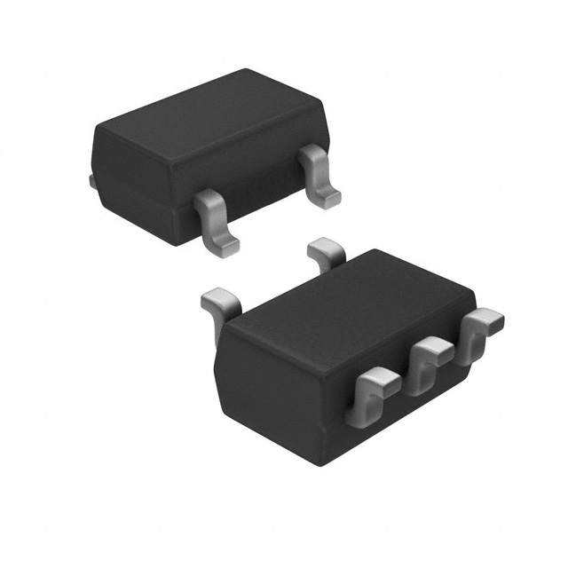


 工商网监
湘ICP备2023018690号
工商网监
湘ICP备2023018690号
