Designated client product
This product will be discontinued its production in the near term.
And it is provided for customers currently in use only, with a time limit.
It can not be available for your new project. Please select other new or
existing products.
For more information, please contact our sales office in your region.
New Japan Radio Co.,Ltd.
www.njr.com
�NJM4562
DUAL OPERATIONAL AMPLIFIER
■ GENERAL DESCRIPTION
The NJM4562 integrated circuit is a high-gain,
wide-bandwidth, low noise, dual operational amplifier capable of
driving 20V peak-to-peak into 600Ω loads. The NJM4562 is
frequency compensated for closed loop gains greater than
10.The NJM4562 combines many of the features of the popular
NJM4558 as well as providing the capability of wider bandwidth,
and higher slew rate and less noise make the NJM4562 ideal
for audio preamplifiers, active filters, telecommunications, and
many instrumentation applications. The availability of the
NJM4562 in the surface mounted micro package allows the
NJM4562 to be used in critical applications requiring very high
packing densities.
■ FEATURES
● Operating Voltage
● Low Input Noise Voltage
● Package Outline
● Bipolar Technology
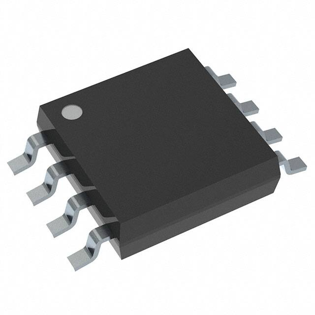
■ PACKAGE OUTLINE
NJM4562D
NJM4562M
( ±4V~±18V )
( 0.6µVrms typ. )
DIP8,DMP8
■ PIN CONFIGURATION
NJM4562D
NJM4562M
PIN FUNCTION
1.A OUTPUT
2.A –INPUT
3.A +INPUT
4.V5.B +INPUT
6.B –INPUT
7.B OUTPUT
8.V+
■ EQUIVALENT CIRCUIT ( 1/2 Shown )
Ver.2011-07-20
-1-
�NJM4562
■ ABSOLUTE MAXIMUM RATINGS
( Ta=25˚C )
PARAMETER
Supply Voltage
Differential Input Voltage
Input Voltage
SYMBOL
V+/VVID
VIC
Power Dissipation
PD
Operating Temperature Range
Storage Temperature Range
Topr
Tstg
RATINGS
± 18
± 30
± 15 ( note )
( DIP8 ) 500
( DMP8 ) 300
-40~+85
-40~+125
UNIT
V
V
V
mW
˚C
˚C
( note ) For supply voltage less than ±15V,the absolute maximum input voltage is equal to the supply voltage.
■ ELECTRICAL CHARACTERISTICS
( Ta=25˚C,V+/V-=±15V )
PARAMETER
Input Offset Voltage
Input Offset Current
Input Bias Current
Input Resistance
Large Signal Voltage Gain
Maximum Output Voltage Swing 1
Maximum Output Voltage Swing 2
Input Common Mode Voltage Range
Common Mode Rejection Ratio
Supply Voltage Rejection Ratio
Operating Current
Equivalent Input Noise Voltage
-2-
SYMBOL
VIO
IIO
IB
RIN
AV
VOM1
VOM2
VICM
CMR
SVR
ICC
VNI
TEST CONDITION
RS≤10kΩ
RL≥2kΩ,VO=±10V
RL≥10kΩ
RL≥2kΩ
RS≤10kΩ
RS≤10kΩ
RS=300Ω,JISA
MIN.
0.3
86
± 12
± 10
± 12
70
76.5
-
TYP.
0.5
5
100
5
110
± 14
± 13
± 14
90
90
3.5
0.6
MAX.
6
200
500
5.7
-
UNIT
mV
nA
nA
MΩ
dB
V
V
V
dB
dB
mA
µVrms
Ver.2011-07-20
�NJM4562
■ TYPICAL CHARACTERISTICS
Ver.2011-07-20
-3-
�NJM4562
■ TYPICAL CHARACTERISTICS
[CAUTION]
The specifications on this databook are only
given for information , without any guarantee
as regards either mistakes or omissions. The
application circuits in this databook are
described only to show representative usages
of the product and not intended for the
guarantee or permission of any right including
the industrial rights.
-4-
Ver.2011-07-20
�
很抱歉,暂时无法提供与“NJM4562M-TE2”相匹配的价格&库存,您可以联系我们找货
免费人工找货