2D_024_010A Data Sheet
2D_024_010A 24V 10W DC-DC Converter
The Helix Semiconductors MuxCapacitor®
2D_024_010A is a member of the MxC® 200
family of monolithic configurable high
voltage switch capacitor DC-DC converters
targeted for use in both non-isolated and
isolated, buck or boost converter
applications. The 2D_024_010A supports a
seamless interface to transformerless
isolated (TL) low voltage PoL regulators to
provide highly efficient DC-DC converter
solutions with 10V to 28.5V input voltages
for regulated or non-regulated PoL
solutions.
Consisting of two unique
capacitive conversion stages, each capable
of providing a separate output voltage, the
2D_024_010A can easily be configured to
support TL systems with multiple voltage
requirements. Intelligent timing & control
optimize power delivery efficiency from noload to maximum power.
Applications
•
•
•
•
•
•
•
•
•
•
•
•
•
PoE: Wireless Access Points, Security
Cameras, VoIP Phones
IoT & IIoT Gateways
Electric & Hybrid Automobiles
Industrial Controllers, HVAC
Telecom, Data Center Functions
24V to 12V Input/Output Voltage
o MuxCap™, G=1/2
o Up to 28V Input Voltage
o Up to 2 outputs
24V to 48V Input/Output Voltage
Up to 10W Output
o Pout = Pout2A + Pout2B
Idle Operation: Active, No-Load
o 1mW Non-Switching
o 48mW Switching
24V to 12V peak efficiency of >96%
o > 90% Efficiency @ 10W
Maximizes PoL regulator efficiency
Fault Detection
o Output Over Current
o Thermal Shutdown
Evaluation Boards, Reference Designs
o Transformerless Isolation - TL
o Unregulated and Regulated
Package Options
o 32 pin QFN, 5mm x 5mm
o Wire Bond Die
MuxCap2A&B Efficiency vs
Load Current
Efficiency (%)
•
Features
100
95
90
85
0
0.5
1
1.5
ILoad (A)
Helix Semiconductors, 2019 All Rights Reserved
1
3.4.19
�2D_024_010A Data Sheet
Table of Contents
1
2
3
4
5
5.1
5.2
5.3
5.4
5.5
6
7
7.1
7.2
8
Pin Configuration and Description ........................................................................................................ 3
Absolute Maximum Ratings .................................................................................................................. 5
Recommended Operating Conditions................................................................................................... 5
Electrical Specifications......................................................................................................................... 6
Functional Description .......................................................................................................................... 9
MuxCapacitor Voltage Divider .............................................................................................................. 9
Low Drop-Out Voltage Regulator ........................................................................................................ 10
Under-Voltage Lockout and POR ........................................................................................................ 10
Clock Generator .................................................................................................................................. 10
Thermal Shutdown.............................................................................................................................. 10
Reference System Application ............................................................................................................ 11
Package Drawings ............................................................................................................................... 15
QFN32 Package .................................................................................................................................. 16
Wire-bond Die .................................................................................................................................... 16
Ordering Information .......................................................................................................................... 17
Table of Tables
Table 1: 2D_024_010A Pin Assignments ...................................................................................................... 3
Table 2: 2D_024_010A Absolute Maximum Ratings .................................................................................... 5
Table 3: 2D_024_010A Recommended Operating Conditions ..................................................................... 5
Table 4: 2D_024_010A Electrical Characteristics.......................................................................................... 6
Table 5: 2D_024_010A Ordering Information ............................................................................................ 17
Table 6: Revision History ............................................................................................................................. 18
Table of Figures
Figure 1: 2D_024_010A QFN32 Pinout ......................................................................................................... 3
Figure 2: VOUT2A, VOUT2B Efficiency .......................................................................................................... 7
Figure 3: VOUT vs Frequency Efficiency........................................................................................................ 7
Figure 4: 2D_024_010A Block Diagram ........................................................................................................ 8
Figure 5: 2D_024_010A Functional Block Diagram....................................................................................... 9
Figure 6: 2D_024_010A Application Schematic .......................................................................................... 12
Figure 7: 2D_024_010A QFN32 Package Drawing ...................................................................................... 16
Helix Semiconductors, 2019 All Rights Reserved
2
3.4.19
�2D_024_010A Data Sheet
1
Pin Configuration and Description
Figure 1: 2D_024_010A QFN32 Pinout
Table 1: 2D_024_010A Pin Assignments
Pin No.
1
Name
VOUT1
3
EN
5
VDD
6
7
GND
VOUTLDO
8
VINLDO
11
RT
12
EXTCLKSEL
Description
MuxCapacitor 1: Output Pin
Attach output capacitor from VOUT1 to PGND1.
Device Enable: Input Pin, Internal 2MΩ Pull-Down, 60Vmax
0 = Disable, 1 = Enable
Pre-Regulator: Output supply voltage pin
Attach 0.1µF capacitor from VDD pin to GND
GND for internal reference and analog circuitry
LDO: 5V Analog Output pin
Attach 4.7µF capacitor from VOUTLDO pin to GND
LDO: Input supply voltage pin
Connect VINLDO pin to VOUT1
Charge Pump Frequency: Input Pin
Add external resistor from RT pin to GND.
External Clock Sync Enable: Input Pin, Internal 2MΩ Pull-Down,
30Vmax
0 = Internal Clock, 1 = External Clock
Helix Semiconductors, 2019 All Rights Reserved
3
3.4.19
�2D_024_010A Data Sheet
13
16
17
18
EXTCLK
PGND2B
CFLY2BB
VOUT2B
19
20
24
25
26
CFLY2BT
VIN2B
PGND2A
CFLY2AB
VOUTA2
27
28
29
30
31
32
2,4,9,10,
14,15,21,
22,23
CFLY2AT
VIN2A
PGND1
CFLY1B
VIN1
CFLY1T
NC
Thermal Pad
External Clock Sync: Input pin, Internal 2MΩ Pull-Down
Power GND
MuxCapacitor 2B: Bottom of flying capacitor
MuxCapacitor 2B: Output Pin
Attach output capacitor from VOUT2B to PGND2B.
MuxCapacitor 2B: Top of flying capacitor
MuxCapacitor 2B: DC input voltage supply pin
Power GND
MuxCapacitor 2A: Bottom of flying capacitor
MuxCapacitor 2A: Output Pin
Attach output capacitor from VOUT2A to PGND2A.
MuxCapacitor 2A: Top of flying capacitor
MuxCapacitor 2A: DC input voltage supply pin
Power GND
MuxCapacitor 1: Bottom of flying capacitor
MuxCapacitor 1: DC input voltage supply pin
MuxCapacitor 1: Top of flying capacitor
No Connect
Power GND
Helix Semiconductors, 2019 All Rights Reserved
4
3.4.19
�2D_024_010A Data Sheet
2
Absolute Maximum Ratings
The 2D_024_010A can be exposed to the following extremes without permanent damage to device
operation. Performance is not guaranteed at these extremes. Continuous operation at these
extremes reduces long term reliability.
Table 2: 2D_024_010A Absolute Maximum Ratings
Pin
VIN1, EN
VIN2, VIN3
VINLDO
EXTCLK
VOUTLDO, VDD, EXTCLKSEL, RT
GND to PGND
ESD Voltage: Human Body Model
ESD Voltage: Charge coupled Model
ESD Voltage: Machine Model
Storage temperature
Junction Temperature
3
Min
-0.3
-0.3
-0.3
-0.3
-0.3
-0.3
-40
-40
Max
62
31
15
30
6
0.3
2
500
200
125
125
Unit
V
V
V
V
V
V
kV
V
V
°C
°C
Recommended Operating Conditions
The 2D_024_010A chip is designed to operate within the design limits specified in the Parametric
Specifications when the conditions of the following table are not exceeded.
Table 3: 2D_024_010A Recommended Operating Conditions
Definition
Input Voltage
Output Power
EN
EXTCLK
EXTCLKSEL, RT
Junction Temperature
Min
20
0
0
0
0
-40
Helix Semiconductors, 2019 All Rights Reserved
5
Max
57
15
57
29
5.5
125
Unit
V
W
V
V
V
°C
3.4.19
�2D_024_010A Data Sheet
4
Electrical Specifications
The electrical characteristics of the Helix Semiconductors 2D_024_010A is tested according to the
following criteria:
Unless otherwise stated, these specifications apply over:
10V < VIN1 < 28.5V, 10V < VIN2A & VIN2B < 28.5V,
4.5V < VOUTLDO < 5.5, Fsw=100kHz, -40·C < TJ < 85͘͘ ·C.
Notes:
1. Min and Max values are valid over Operating Conditions, unless otherwise stated.
2. Typ values are valid at typical Operating Conditions and typical process Parameters.
3. Guaranteed by Design.
Table 4: 2D_024_010A Electrical Characteristics
Symbol
Parameter
Condition
Min
Typ
Max
Unit
0.3
V
A
mΩ
1
300
V
A
mΩ
5
V
60V MuxCapacitor Voltage Divider: VIN1/VOUT1
Vout
Iout
Rsw
Output Voltage
Output Current
Switch Rdson
VIN=4V, Po=0W, Note 3.
Note 3.
48
600
30V MuxCapacitor Voltage Divider: VIN2A/VOUT2A and VIN2B/VOUT2B
Vout
Iout
Rsw
Output Voltage
Output Current
Switch Rdson
VIN=24V, Po=0W, Note 3.
Note 3.
12
VOUTLDO
VoutLDO
Output Voltage
Under Voltage Lockout
UVVoutS+
UVVoutSEN+
EN1
VOUTLDO Start
VOUTLDO Stop
Enable On Thresh.
Enable Off Thresh.
5V Rising Trip Level
5V Falling Trip Level
Enable Rising Trip Level
Enable Falling Trip Level
4.4
4.1
1.14
0.95
4.6
4.2
1.2
1.0
4.8
4.3
1.26
1.05
V
V
V
V
95
230
kHz
Clock Generator
Fsw
Switching Frequency RT=402KΩ,95kHz
RT=174KΩ, 220kHz
Thermal Shutdown
TSD
Hyst
Thermal Shutdown
Hysteresis
Note 3.
Note 3.
Helix Semiconductors, 2019 All Rights Reserved
6
145
20
°C
°C
3.4.19
�2D_024_010A Data Sheet
Figure 2: VOUT2A, VOUT2B Efficiency
MuxCap2A&B Efficiency vs Load Current
97
96
Efficiency (%)
95
94
93
92
91
90
89
0
0.2
0.4
0.6
0.8
1
1.2
ILoad (A)
Figure 3: VOUT vs Frequency Efficiency
Efficiency (%)
MuxCap2A&B @ 100kHz & 200kHz
Efficiency vs Load Current
97.0
96.0
95.0
94.0
93.0
92.0
91.0
90.0
89.0
88.0
87.0
86.0
100kHz
200kHz
0
0.5
1
1.5
2
ILoad (A)
Helix Semiconductors, 2019 All Rights Reserved
7
3.4.19
�2D_024_010A Data Sheet
Figure 4: 2D_024_010A Block Diagram
Helix Semiconductors, 2019 All Rights Reserved
8
3.4.19
�2D_024_010A Data Sheet
5
Functional Description
The Helix Semiconductors 2D_024_010A DC-DC MuxCapacitor IC is an easy to use, highly efficient DC
voltage divider. It combines three MuxCapacitor Voltage Dividers to reduce the input voltage
allowing the use of lower voltage / lower cost PoL regulators.
Figure 5: 2D_024_010A Functional Block Diagram
Each MuxCapacitor stage has its own input and output pins allowing for multiple configurations. All
three stages can be connected in series for access to intermediate voltage reduction outputs. Or, the
MuxCapacitor stages can be wired in parallel for added output current capability and efficiency.
5.1
MuxCapacitor Voltage Divider
The 2D_024_010A Muxcapacitor Voltage Dividers (MCVD) divide the DC voltage present at the
VIN2A&B pins to reduced voltages at the VOUT2A, and VOUT2B pins which provides the input voltage
to an external POL regulator. Also, the input voltage present at VIN1 is doubled at the VOUT1 output.
The MCVD is comprised of two stages, each with a gain of ½ and a third stage with a 2x gain.
Each MCVD uses an external flying capacitor, an internal switching circuit, and an external hold
capacitor. The switching device is configured to operate the corresponding voltage reduction circuit
at charging and discharging phases from a two-phase non-overlapping on-chip clock generator.
Helix Semiconductors, 2019 All Rights Reserved
9
3.4.19
�2D_024_010A Data Sheet
Each MuxCapacitor contains over-current protection. The over-current protection automatically
resets once the over-current condition clears. This feature is active at startup enhancing the softstart ramp-up at each VOUTx.
5.2
Low Drop-Out Voltage Regulator
An integrated 5V LDO provides the supply voltage for the analog circuits. The 5V LDO is powered
from the VINLDO pin. The VINLDO supply voltage range is 7-15V.
The 5V LDO uses the bandgap output as the reference voltage to generate the desired output voltage.
5.3
Under-Voltage Lockout and POR
The integrated under-voltage lockout circuit monitors the voltages at the 5V LDO output, and the
Enable pin. It ensures that the MuxCapacitor outputs remain in the off state whenever one of these
signals drop below the set thresholds. Normal operation resumes once these signals rise above their
thresholds. The Power-On Ready (POR) signal is generated when each signal reaches their valid logic
level. When the POR is asserted the Soft-Start sequence starts. All the UVLO comparators except the
enable circuit are disabled when enable is low to achieve the ultra-low power dissipation.
5.4
Clock Generator
The integrated clock generator’s switching frequency is programmed with an external resistor (402KΩ
typical) connected from the RT pin to GND. The MuxCapacitor switching frequency (Fsw) is calculated
as:
Fsw (kHz) = 38,190 / External RT Resistor (Kohms)
This clock signal can be synchronized to an external clock by using the EXTCLK pin. Switching activity
at the EXTCLK pin enables the internal synchronizer. When the synchronizer is enabled (EXTCLKSEL
= 1), the MuxCapacitor clock will track the EXTCLK pin switching rate. As the EXTCLK pin frequency
slows down, the MuxCapacitor clock slows down. The EXTCLK signal is derived from the external
POL’s switch drive signal. This allows the MuxCapacitors to save power as the external switcher slows
down due to reduced load demand. The MuxCapacitor switching frequency is ¼ the EXTCLK
frequency.
5.5
Thermal Shutdown
Temperature sensing is included and provides the signal to an over temperature detector. The trip
threshold is set to 145͘͘·C. When trip threshold is exceeded, thermal shutdown turns off the
MuxCapacitor outputs and resets the internal soft start.
Helix Semiconductors, 2019 All Rights Reserved
10
3.4.19
�2D_024_010A Data Sheet
The restart is automatically initiated when the sensed temperature drops down within the normal
operating range. A 20·C hysteresis is incorporated into the thermal shutdown threshold. The thermal
shutdown circuit is disabled when enable is low to achieve the ultra-low power dissipation.
6
Reference System Application
The 2D_024_010A is typically paired with the 2I_048_10A to implement a transformerless isolated
(TL) power supply. The following system diagrams provide 10W TL application schematics. The
2D_024_010A is shown as a simple DC-DC voltage reduction circuit on the secondary side of the
safety barrier isolation interface. Two MuxCapacitor stages are wired in parallel to perform a G=1/2
voltage reduction and improved efficiency. The third MuxCapacitor boosts the input voltage for the
internal high side gate drivers and can be tapped for 48V power. While the total power drawn from
the 2D_024_010A cannot exceed 10W where Pout = Pout2A + Pout2B, each MuxCapacitor cell has a
maximum output current. The Iout_max for VOUT1 cannot exceed 0.1A. The Iout_max for VOUT2A
and VOUT2B cannot exceed 1A individually. The last two stages are 180o out of phase to reduce
ripple.
The MuxCapacitor can be reconfigured as a push/pull driver. This configuration is utilized in the
2I_48_010A’s full bridge driver. Additionally, the push/pull configuration is employed to generate a
negtive voltage as shown in the MxC 273 schematic.
Efficiency and delivered power are dependent on application circuit implementation, capacitor
components, RT frequency and thermal management. Consult the factory for additional design
information.
Helix Semiconductors, 2019 All Rights Reserved
11
3.4.19
�2D_024_010A Data Sheet
Figure 6: 2D_024_010A Application Schematic
MxC 270-EB-C
Helix Semiconductors, 2019 All Rights Reserved
12
3.4.19
�2D_024_010A Data Sheet
MxC 271-EB-C
Helix Semiconductors, 2019 All Rights Reserved
13
3.4.19
�2D_024_010A Data Sheet
MxC 273-EB-C
Helix Semiconductors, 2019 All Rights Reserved
14
3.4.19
�2D_024_010A Data Sheet
MxC 274-EB-C
Helix Semiconductors, 2019 All Rights Reserved
15
3.4.19
�2D_024_010A Data Sheet
7
Package Drawings
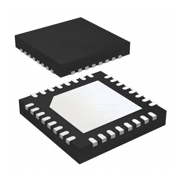
The available packages for the 2D_024_010A are shown in the following drawings.
7.1
QFN32 Package
The 2D_024_010A is packaged in a 32-pin 5mm x 5mm QFN package as shown below.
Figure 7: 2D_024_010A QFN32 Package Drawing
7.2
Wire-bond Die
The 2D_024_010A is available in die form. Please contact factory for information regarding die
sales.
Helix Semiconductors, 2019 All Rights Reserved
16
3.4.19
�2D_024_010A Data Sheet
8
Ordering Information
Refer to the following table for package option ordering information.
Table 5: 2D_024_010A Ordering Information
Part Number
2D-024-10A-QFN32-1
2D-024-10A-WD-1
MxC 270-EB-1
MxC 271-EB-1
MxC 273-EB-1
Description
32 pin 5mm x 5mm QFN
Wire Bond Die
48V to 12V Unregulated TL Evaluation Board
6V to 6V Unregulated TL Evaluation Board
48V to 5V Regulated TL Evaluation Board
Package
QFN
Die
Eval Board
Eval Board
Eval Board
This product is covered by one or more Helix Semiconductors patents.
Patent http://www.helixsemiconductors.com/pages/company/trademarksandpatents
Helix Semiconductors, 2019 All Rights Reserved
17
3.4.19
�2D_024_010A Data Sheet
Table 6: Revision History
Date
1.30.19
2.2.19
3.4.19
Revision
1
2
3
Description
Initial release
Miscellaneous edits
Patent disclosure, PoE schematic
Operational Headquarters
Engineering & Design Office
9980 Irvine Center Drive
Suite 100
Irvine, CA 92618
5475 Mark Dabling Blvd.
Suite 206
Colorado Springs, CO 80918
Information & Sales
719-594-7098
designs@helixsemiconductors.com
949-748-6057
sales@helixsemiconductors.com
Technical Support
949-748-7026
support@helixsemiconductors.com
Corporate Headquarters
4808 West Utica Ave.
Broken Arrow, OK 74011
Helix Semiconductors, 2019 All Rights Reserved
18
3.4.19
�