LM317
3-Terminal Adjustable Output Positive Voltage Regulators
Features
• Output current in excess of 1.5 ampere
• Output adjustable between 1.2V and 37V
• Internal thermal overload protection
• Internal short-circuit current limiting
constant with temperature
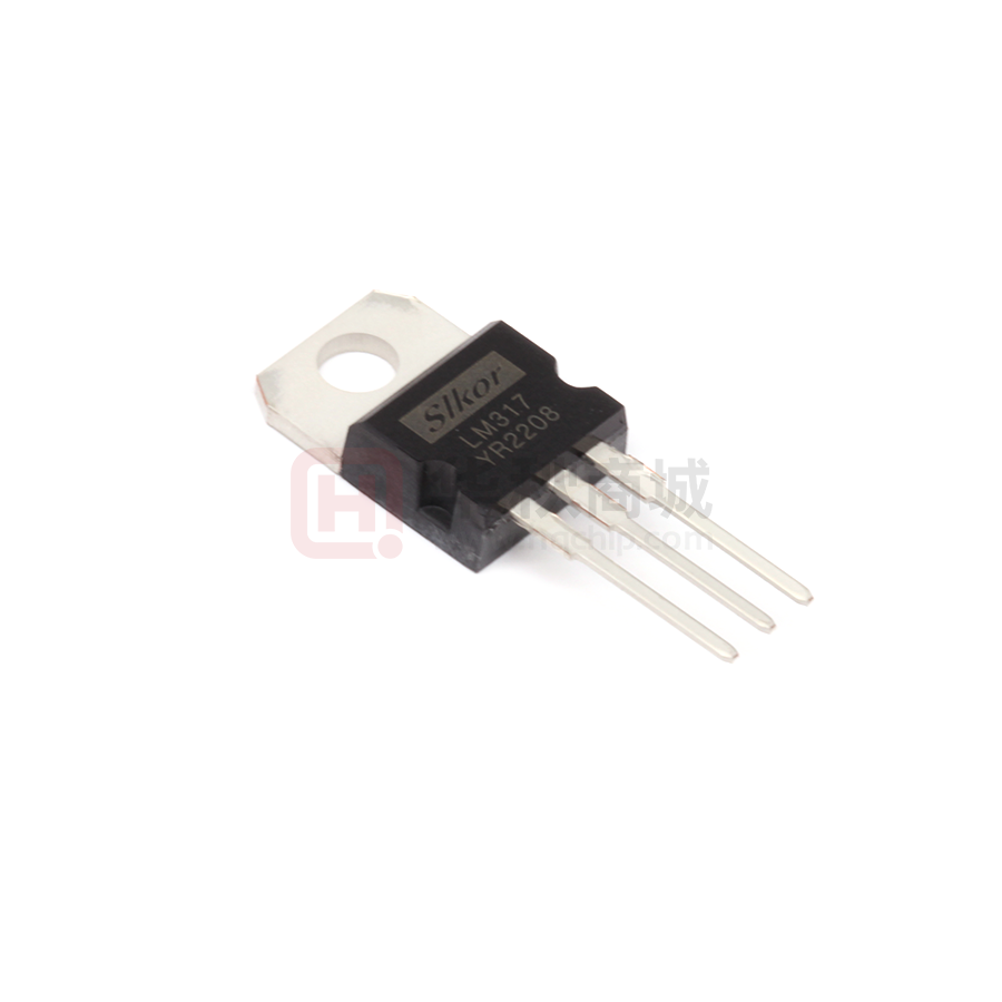
TO-220
• Output transistor safe-area compensation
• Floating operation for high voltage applications
1
3
2
1. Adjust
2. Vout
3. Vin
• Eliminates stocking many fixed voltages
Heatsink is connected to pin 2
Standard Application
Vin
LM317
Cin
0.1µF
Functional Block Diagram
Input
Vout
IADJ
R1
Adjust 240Ω
3
Co
1µF
+
R2
-Notes:
Cin is required if regulator is located an appreciable distance from power
supply filter.
Voltage
Reference
Protection
Circuitry
Rlimit
Co is not needed for stability, however, it does improve transient response.
Vout = 1.25V (1 + R2 / R1) + IAdj R2
1
Since IAdj is controlled to less than 100µA, the error associated with this
term is negligible in most applications
Maximum Ratings
2
Output
Vadj
Ratings at 25°C ambient temperature unless otherwise specified.
Parameter
Symbol
Value
Unit
Vi-Vo
40
Vdc
RθJC
3.0
°C
Power Dissipation, 25°C Case Temperature
PD
15
W
Operating Junction Temperature Range
TJ
0 to +125
°C
Tstg
–65 to +150
°C
Input-Output Voltage Differential
Junction-to-Case Thermal Resistance
Storage Junction Temperature Range
www.slkormicro.com
1
�LM317
Electrical Characteristics
Vi -Vo = 5V, Io = 0.5A, TJ = Tlow to Thigh (see Note 1), Imax and Pmax per Note 2, unless otherwise noted.
Parameter
Symbol
Line Regulation (Fig. 1) (3)
3.0V ≤ VI – Vo ≤ 40V
REG line
Load Regulation (Fig. 2) (3)
TJ = 25°C, 10mA ≤ Io ≤ 1.5A
REG load
Load Regulation (Fig. 2) (3)
10mA ≤ Io ≤ 1.5A
REG load
Thermal Regulation
REG therm
Adjustment Pin Current (Fig. 3)
Conditions
Min.
Typ.
Max.
TA = 25°C
–
0.01
0.04
TJ = 0°C thru 125°C
–
0.02
0.07
Vo ≤ 5.0
–
5
25
mV
Vo ≥ 5.0
–
0.1
0.5
%Vo
Vo ≤ 5.0
–
20
70
mV
Vo ≥ 5.0
–
0.3
1.5
%Vo
TJ = 25°C, 20ms Pulse
–
0.03
0.07
%Vo/W
–
50
100
µA
IAdj
Unit
%Vo/V
Adjustment Pin Current Change
∆IAdj
10mA ≤ IL ≤ 1.5A
2.5V ≤ VI – Vo ≤ 40V
–
0.2
5
µA
Reference Voltage (Fig. 3) (4)
Vref
10mA ≤ Io ≤ 1.5A
3V ≤ VI – Vo ≤ 40V
1.225
1.25
1.275
V
Temperature Stability (Fig. 3)
TS
Tlow ≤ TJ ≤ Thigh
–
1
–
%Vo
Min. Load Current to Maintain Regulation (Fig. 3)
ILmin
VI – Vo = 40V
–
3.5
10
mA
Maximum Output Current (Fig. 3)
Imax
VI – Vo ≤ 15V
1.5
2.2
–
VI – Vo = 40V, TJ = 25°C
0.15
0.4
–
N
TJ = 25°C, 10HZ ≤ f ≤ 10KHZ
—
0.003
–
%Vo
RR
Vo = 10V, f = 120HZ(5)
CAdj = 10µF
—
66
65
80
–
–
dB
S
TJ = 125°C(6), TJ = 25°C for
Endpoint Measurements
–
0.3
1.0
%
RθJC
Tlow ≤ TJ ≤ Thigh
–
5.0
–
°C/W
RMS Noise, % of Vo
Ripple Rejection (Fig. 4)
Long-Term Stability (after 1000 hr)
Fig. 3
Thermal Resistance Junction to Case
Notes:
(1) Tlow = 0°C Thigh = 125°C
(2) Imax = 1.5A Pmax is internally limited
(3) Load and line regulation are specified at constant junction temperature. Changes in Vo due to heating effects must be taken into account separately.
Pulse testing with low duty cycle is used.
(4) Selected devices with tightened tolerance reference voltage available.
www.slkormicro.com
2
A
�LM317
Fig. 1 – Line Regulation Test Circuit
Fig. 2 – Load Regulation and
∆Iadj /Load Test Circuit
V
V
Line Regulation (%/V) = OH -- OL x100
VOL
VIH
VIL
Vin
Load Regulator (mV) = Vo(min. Load) -- Vo(max. Load)
Vo(min. Load) -- Vo(max. Load)
Load Regulator (%Vo) =
x100
Vo(min. Load)
VOH
VOL
Vout
VI
Vin
LM317
IADJ
IL
LM317
240Ω
1%
Adjust R1
IADJ
Co
Adjust R1
240Ω
1%
Cin
RL
Cin
0.1µF
VOH (min. Load)
VOL (max. Load)
Vout
1µF
0.1µF
R2
1%
Pulse Testing Required:
1% Duty Cycle is Suggested
RL
(min.
Load)
Co
1µF
R2
1%
Pulse Testing Required:
1% Duty Cycle is Suggested
Fig. 3 – Standard Test Circuit
Fig. 4 – Ripple Rejection Test Circuit
24V
14V
f = 120HZ
Vin
Vin
Vout
IL
LM317
IADJ
VI
Adjust R1
240
1%
R1
Vref
Adjust
Cin
Co
0.1µF
1µF
240
1%
*D1
1N4002
Co
Vo
RL
0.1µF
R2
1%
www.slkormicro.com
Vo = 10V
Cin
RL
ISET
Pulse Testing Required:
1% Duty Cycle is Suggested
Vout
LM317
CAdj
R2
1%
To Calculate R2:
Vo = ISET R2 + 1.250V
Assume ISET = 5.25mA
*D1 Discharges CADJ if
Output is Shorted to Ground
3
10µF
1µF
Vo
�LM317
Ratings and
Characteristic Curves (T
A
= 25°C unless otherwise noted)
Fig. 6 – Current Limit
Fig. 5 – Load Regulation
4
0.4
0.2
Io -- Output Current (A)
∆Vo -- Output Voltage Change (%)
0.6
IL = 0.5A
0
--0.2
IL = 1.5A
--0.4
--0.6
VI = 15V
Vo = 10V
3
TJ = 25°C
2
1
--0.8
--1.0
--75
0
--50 --25
0
25
50
75
0
100 125 150 175
10
Fig. 7 – Adjustment Pin Current
30
40
Fig. 8 – Dropout Voltage
VI -- Vo -- Input -- Output Voltage
Differential (Vdc)
70
65
60
55
50
45
40
35
--75
20
3.0
75
IADJ -- Adjustment Pin Current (µA)
TJ = --55°C
TJ = 150°C
--50 --25
0
25
50
75
∆Vo = 100mV
2.5
IL = 1.5A
IL = 1.0A
2.0
IL = 500mA
1.5
IL = 200mA
IL = 20mA
1.0
--75
100 125 150 175
Fig. 9 – Temperature Stability
--50 --25
0
25
50
75
100 125 150 175
Fig. 10 – Minimum Operating Current
5.0
1.260
IO -- Quiescent Current (mA)
Vref -- Reference Voltage (V)
4.5
1.250
1.240
1.230
4.0
TJ = 25°C
3.5
TJ = --55°C
TJ = 150°C
3.0
2.5
2.0
1.5
1.0
0.5
1.220
--75
0
--50 --25
0
www.slkormicro.com
25
50
75
100 125 150 175
0
4
10
20
30
40
50
�LM317
Ratings and
Characteristic Curves (T
A
= 25°C unless otherwise noted)
Fig. 12 – Ripple Rejection
vs. Output Current
Fig. 11 – Ripple Rejection
vs. Output Voltage
140
100
120
80
RR -- Ripple Rejection (db)
RR -- Ripple Rejection (db)
CAdj = 10µF
Without CAdj
60
40
VI -- Vo = 5V
IL = 500mA
f = 120HZ
TJ = 25°C
20
0
0
5
10
15
20
25
30
35
CAdj = 10µF
100
80
Without CAdj
60
40
VI = 15V
Vo = 10V
f = 120HZ
TJ = 25°C
20
0
0.01
40
0.1
Fig. 13 – Ripple Rejection
vs. Frequency
Fig. 14 – Output Impedance
100
101
VI = 15V
Vo = 10V
IL = 500mA
TJ = 25°C
80
Output Impedance (Ω)
RR -- Ripple Rejection (db)
10
Io -- Output Current (A)
Vo -- Output Voltage (V)
CAdj = 10µF
60
Without CAdj
40
IL = 500mA
VI = 15V
Vo = 10V
TJ = 25°C
20
0
10
100
100
10--1
Without CAdj
10--2
CAdj = 10µF
1K
10K
100K
10--3
10
1M
100
f -- Frequency (Hz)
1K
10K
100K
1M
f -- Frequency (Hz)
Fig. 15 – Line Transient Response
Fig. 16 – Load Transient Response
Vo -- Output Voltage
Deviation (V)
3
1.5
1.0
CL = 1µF CAdj = 10µF
0.5
0
--0.5
Vo = 10V
IL = 50mA
TJ = 25°C
--1.0
2
1
CL = 1µF CAdj = 10µF
0
--1
--2
CL = 0 Without CAdj
--3
IL -- Load
Current (A)
∆VI -- Input Voltage ∆Vo -- Output Voltage
Change (V)
Deviation (V)
1
CL = 0
Without CAdj
--1.5
1.0
VI
0.5
0
VI = 15V
Vo = 10V
INL = 50mA
TJ = 25°C
1.5
1.0
IL
0.5
0
0
10
20
30
40
0
t -- Time (µs)
www.slkormicro.com
10
20
t -- Time (µs)
5
30
40
�LM317
TO-220 Case Outline
10.25 ± 0.25
4.85 ±
0.375
1.27
± 0.12
3.84 ± 0.6 Dia.
2.69 ± 0.25
6.26 ± 0.25
14.8 ± 0.51
8.54 ± 0.26
28.7 ± 0.92
3.94 ± 0.375
13.9 ± 0.41
Dimensions in
millimeters
2.53
± 0.185
www.slkormicro.com
1.3 ± 0.185
0.387 ± 0.09
2.55
± 0.375
0.8 ± 0.12
6
�
很抱歉,暂时无法提供与“LM317”相匹配的价格&库存,您可以联系我们找货
免费人工找货- 国内价格
- 5+2.55258
- 50+1.95016
- 150+1.72152
- 500+1.43630
- 2500+1.30929
- 5000+1.23304