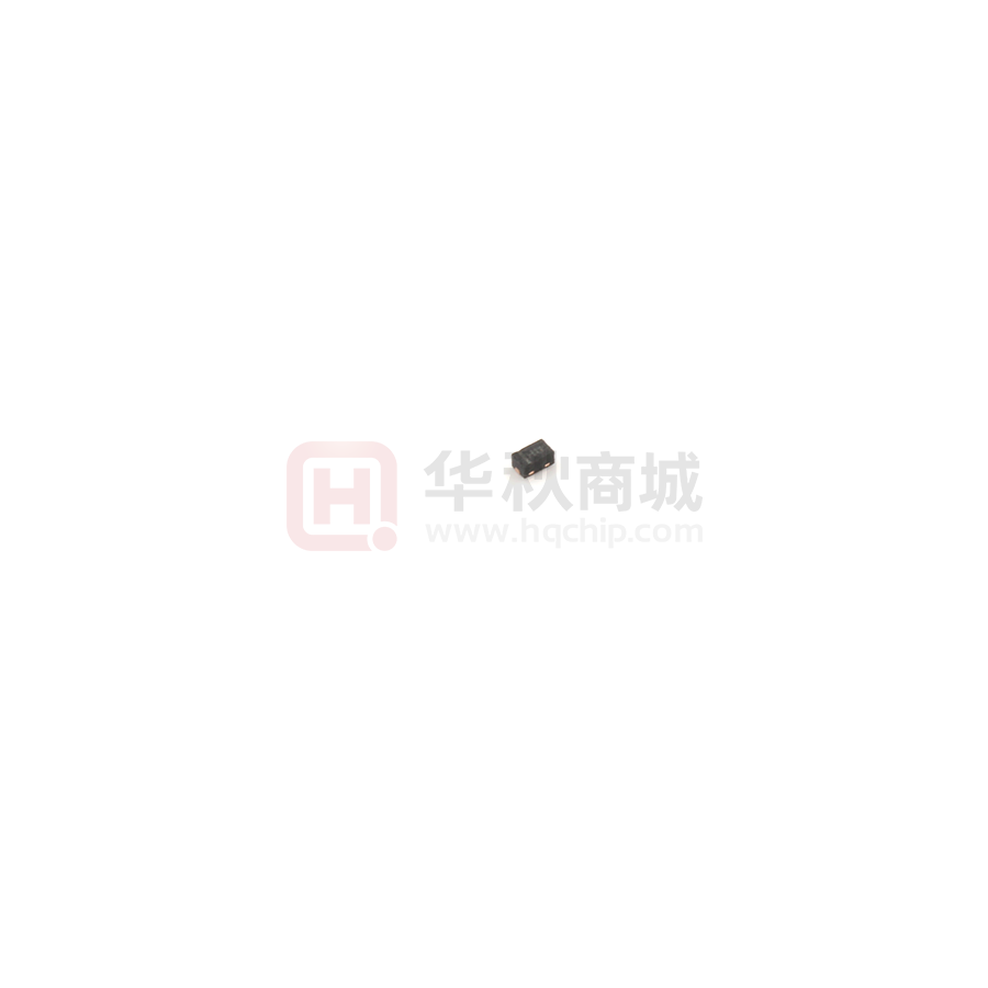
ESD9N5BU
ESD9N5BU
http//:www.sh-willsemi.com
1-Line, Bi-directional, Ultra-low Capacitance,
Transient Voltage Suppressor
Descriptions
The ESD9N5BU is a transient voltage suppressors (TVS)
which provide a very high level protection for sensitive
electronic components that may be subjected
to
electrostatic discharge (ESD). It is designed to replace
DFN1006-2L (Bottom View)
multiplayer varistors (MLV) in consumer equipments
applications such as mobile phone, notebook, PAD, STB,
LCD TV etc.
The ESD9N5BU was past ESD transient voltage up to
±12KV
(contact)
according
to
IEC61000-4-2
and
Pin2
Pin1
withstand peak current up to 3A for 8/20μs pulse
according to IEC61000-4-5.
The ESD9N5BU is available in DFN1006 package.
Standard products are Pb-free and Halogen-free.
Circuit Diagram
Features
Reverse stand-off voltage: ±5.0V max.
Transient protection for each line according to
IEC61000-4-2 (ESD)
: ±12kV (contact discharge)
IEC61000-4-4 (EFT)
:40A (5/50ns)
: ±15kV (air discharge)
IEC61000-4-5 (surge) :3A (8/20μs)
Ultra-low capacitance
Low clamping voltage
Low leakage current
Small package
Mobile phone
PAD
Notebook
STB
LCD TV
Digital camera
Other electronics equipments
Will Semiconductor Ltd.
*
= Month (A~Z)
U
= Device code
Pin2
Marking (Top View)
Order information
Applications
*U
Pin1
1
Device
Package
Shipping
ESD9N5BU-2/TR
DFN1006-2L
10000/Tape&Reel
Revision 2.2, 2014/10/14
�ESD9N5BU
Absolute maximum ratings
Parameter
Symbol
Rating
Unit
Peak pulse power (tp=8/20μs)
Ppk
54
W
Peak pulse current (tp=8/20μs)
Ipp
3
A
ESD voltage IEC61000-4-2 air
±15
VESD
ESD voltage IEC61000-4-2 contact
Junction temperature
TJ
Operating temperature
TOP
Lead temperature
TL
Storage temperature
KV
±12
Tsg
125
o
-40~85
o
260
o
-55~150
o
C
C
C
C
Electronics characteristics (Ta=25 oC, unless otherwise noted)
Parameter
Symbol
Reverse stand-off voltage
VRWM
Reveres leakage current
IR
Reveres breakdown voltage
Clamping voltage
1)
Dynamic resistance
1)
Condition
Min.
Typ.
VRWM = 5V
VBR
IT = 1mA
7.0
VCL
IPP = 16A, tp = 100ns
RDYN
8.5
Max.
Unit
±5.0
V
1.0
μA
10.0
V
35
V
1.61
Ω
Clamping voltage
2)
VCL
VESD = 6kV
27
V
Clamping voltage
2)
VCL
VESD = 8kV
35
V
Clamping voltage
3)
VC
Junction capacitance
CJ
Ipp=1A tp=8/20us
11.8
14
V
Ipp=3A tp=8/20us
16
18
V
F=1MHz, VR=0V
0.45
0.7
pF
Notes:
1) TLP parameter: Z0 = 50Ω , tp = 100ns, tr = 2ns, averaging window from 60ns to 80ns. RDYN is calculated from 4A to
16A.
2)
Contact discharge mode, according to IEC61000-4-2.
3)
Non-repetitive current pulse, according to IEC61000-4-5.
Will Semiconductor Ltd.
2
Revision 2.2, 2014/10/14
�ESD9N5BU
o
100
90
Front time: T1= 1.25 × T = 8µs
Time to half-value: T2= 20µs
100
90
Current (%)
Peak pulse current (%)
Typical characteristics (TA=25 C, unless otherwise noted)
50
T2
10
10
0
0
T
T1
tr = 0.7~1ns
Time (µs)
20
0.6
C - Junction capacitance (pF)
Pulse waveform: tp=8/20us
VC - Clamping voltage (V)
Time (ns)
Contact discharge current waveform per IEC61000-4-2
8/20μs waveform per IEC61000-4-5
16
12
8
4
t
60ns
30ns
20
0
1
2
3
Ipp - Peak pulse current (A)
Fsignal=1MHz
0.5
Vsignal=50mVrms
0.4
0.3
0.2
4
0
Clamping voltage vs. Peak pulse current
1
2
3
4
VR - Reverse voltage (V)
5
Capacitance vs. Reverse voltage
1000
% of Rated power
Peak Pulse Power (W)
100
100
10
80
60
40
20
1
0
1
10
100
Pulse Duration(us)
1000
25
50
75
100
125
150
o
TA - Ambient temperature ( C)
Non-repetitive peak pulse power vs. Pulse time
Will Semiconductor Ltd.
0
Power derating vs. Ambient temperature
3
Revision 2.2, 2014/10/14
�ESD9N5BU
o
Typical characteristics (TA=25 C, unless otherwise noted)
ESD clamping
ESD clamping
(-8kV contact discharge per IEC61000-4-2)
(+8kV contact discharge per IEC61000-4-2)
20
TLP current (A)
15
10
5
0
-5
Z0 = 50 Ω
tr = 2ns
tp = 100ns
-10
-15
-20
-40 -30 -20 -10 0 10 20
TLP voltage (V)
30
40
TLP Measurement
Will Semiconductor Ltd.
4
Revision 2.2, 2014/10/14
�ESD9N5BU
Package outline dimensions
DFN1006-2L
Top View
Bottom View
Side View
Min.
Typ.
Max.
A
0.30
-
0.50
A1
0.00
-
0.05
A3
0.125 Ref.
D
0.95
1.00
1.05
E
0.55
0.60
0.65
b
0.20
0.25
0.30
L
0.45
0.50
0.55
e
0.65 Typ.
Recommend land pattern (Unit: mm)
Notes:
This recommended land pattern is for reference
purposes only. Please consult your manufacturing
group to ensure your PCB design guidelines are met.
Will Semiconductor Ltd.
5
Revision 2.2, 2014/10/14
�
很抱歉,暂时无法提供与“ESD9N5BU-2/TR”相匹配的价格&库存,您可以联系我们找货
免费人工找货- 国内价格
- 5+0.14681
- 20+0.14412
- 100+0.13873
