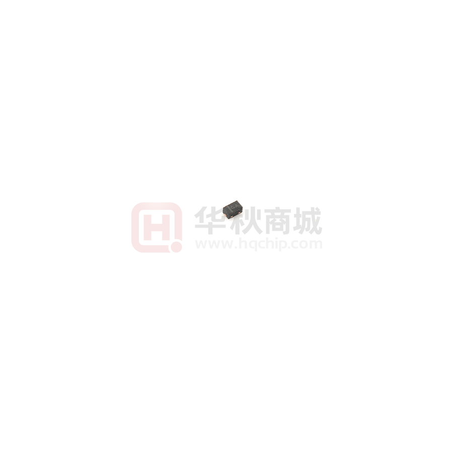
ESD9N12BA
ESD9N12BA
1-Line, Bi-directional, Transient Voltage Suppressors
http//:www.sh-willsemi.com
Descriptions
The ES9DN12BA is a TVS (Transient Voltage Suppressor)
designed to protect sensitive electronic components which
are connected to data and transmission lines from
over-stress caused by ESD (Electrostatic Discharge), EFT
(Electrical Fast Transients) and lightning.
DFN1006-2L (Bottom View)
The ESD9N12BA may be used to provide ESD protection up
to ±30kV (contact discharge) according to IEC61000-4-2,
and withstand peak pulse current up to 5.5A (8/20μs)
according to IEC61000-4-5.
Pin1
Pin2
The ESD9N12BA is available in DFN1006-2L package.
Standard products are Pb-free and Halogen-free.
Circuit diagram
Features
Stand-off voltage: ±12V Max.
Transient protection for each line according to
Pin1
IEC61000-4-2 (ESD): ±30kV (contact discharge)
*A
Pin2
IEC61000-4-5 (surge): 5.5A (8/20μs)
Capacitance: CJ = 27pF typ.
Ultra-low leakage current: IR = 0.1nA typ.
Low clamping voltage: VCL = 20V typ. @ IPP = 16A (TLP)
Solid-state silicon technology
A = Device code
* = Month code ( A~Z)
Marking (Top View)
Applications
Computers and peripherals
Cellular handsets
Portable Electronics
Notebooks
Will Semiconductor Ltd.
Order information
Device
Package
Shipping
ESD9N12BA-2/TR DFN1006-2L 10000/Tape&Reel
1
Revision 1.5, 2018/04/23
�ESD9N12BA
Absolute maximum ratings
Parameter
Symbol
Rating
Unit
Peak pulse power (tp = 8/20μs)
Ppk
99
W
Peak pulse current (tp = 8/20μs)
IPP
5.5
A
ESD according to IEC61000-4-2 air discharge
±30
VESD
kV
ESD according to IEC61000-4-2 contact discharge
±30
TJ
125
o
Operating temperature
TOP
-40~85
o
Lead temperature
TL
260
o
TSTG
-55~150
o
Junction temperature
Storage temperature
C
C
C
C
Electrical characteristics (TA=25 oC, unless otherwise noted)
Parameter
Stand-off voltage
Reverse breakdown voltage
1)
Dynamic resistance
Clamping voltage
Condition
Min.
Typ.
VRWM
Reverse leakage current
Clamping voltage
Symbol
1)
2)
Junction capacitance
IR
VRWM = 12V
VBR
IT = 1mA
VCL
IPP = 16A, tp = 100ns
RDYN
VCL
0.1
13
Max.
Unit
±12
V
50
nA
16.5
V
20
V
0.35
Ω
IPP = 1A, tp = 8/20μs
16
V
IPP = 5.5A, tp = 8/20μs
18
V
VR = 0V, f = 1MHz
27
35
pF
VR = 12V, f = 1MHz
14
20
pF
CJ
1) TLP parameter: Z0 = 50Ω, tp = 100ns, tr = 2ns, averaging window from 60ns to 80ns. RDYN is calculated from 4A to
16A.
2)
Non-repetitive current pulse, according to IEC61000-4-5.
Will Semiconductor Ltd.
2
Revision 1.5, 2018/04/23
�ESD9N12BA
o
100
90
Front time: T1= 1.25 T = 8s
100
90
Time to half-value: T2= 20s
Current (%)
Peak pulse current (%)
Typical characteristics (TA=25 C, unless otherwise noted)
50
T2
10
10
0
0
tr = 0.7~1ns
Time (s)
T1
CJ - Junction capacitance (pF)
VC - Clamping voltage (V)
28
Pulse waveform: tp = 8/20s
19
18
17
16
15
14
13
0
1
2
3
4
Time (ns)
Contact discharge current waveform per IEC61000-4-2
8/20μs waveform per IEC61000-4-5
20
t
60ns
30ns
20
T
5
6
f = 1MHz
VAC = 50mV
26
24
22
20
18
16
14
12
7
0
2
IPP - Peak pulse current (A)
4
6
8
10
12
VR - Reverse voltage (V)
Clamping voltage vs. Peak pulse current
Capacitance vs. Reverse voltage
1000
% of Rated power
Peak pulse power (W)
100
100
10
1
10
100
Pulse time (s)
60
40
20
0
1000
0
25
50
75
100
125
150
o
TA - Ambient temperature ( C)
Non-repetitive peak pulse power vs. Pulse time
Will Semiconductor Ltd.
80
Power derating vs. Ambient temperature
3
Revision 1.5, 2018/04/23
�ESD9N12BA
o
Typical characteristics (TA=25 C, unless otherwise noted)
ESD clamping
ESD clamping
(+8kV contact discharge per IEC61000-4-2)
(-8kV contact discharge per IEC61000-4-2)
TLP current (A)
20
18
Z0 = 50
16
tr = 2ns
14
tp = 100ns
12
10
8
6
4
2
0
0
2
4
6
8
10 12 14 16 18 20 22
TLP voltage (V)
TLP Measurement
Will Semiconductor Ltd.
4
Revision 1.5, 2018/04/23
�ESD9N12BA
PACKAGE OUTLINE DIMENSIONS
DFN1006-2L
b
L
E
(Ⅰ)
(Ⅱ)
(Ⅲ)
D
e
Top View
Bottom View
(Ⅰ)
A3
A1
A
(Ⅱ)
Side View
Dimensions in Millimeters
Symbol
Min.
Typ.
Max.
A
0.34
0.45
0.53
A1
0.00
0.02
0.05
A3
0.12 Ref.
D
0.95
1.00
1.08
E
0.55
0.60
0.68
b
0.20
0.25
0.30
L
0.45
0.50
0.55
e
0.65 BSC
Recommended land pattern (Unit: mm)
0.55
0.60
0.30
Notes:
0.85
This recommended land pattern is for reference
purposes only. Please consult your manufacturing
1.40
Will Semiconductor Ltd.
group to ensure your PCB design guidelines are met.
5
Revision 1.5, 2018/04/23
�ESD9N12BA
TAPE AND REEL INFORMATION
RD
Reel Dimensions
Tape Dimensions
W
P1
Quadrant Assignments For PIN1 Orientation In Tape
Q1
Q2
Q1
Q2
Q3
Q4
Q3
Q4
RD
Reel Dimension
W
Overall width of the carrier tape
P1
Pitch between successive cavity centers
Pin1
Pin1 Quadrant
Will Semiconductor Ltd.
User Direction of Feed
7inch
13inch
1 8mm
12mm
16mm
2mm
4mm
8mm
Q1
Q2
Q3
6
Q4
Revision 1.5, 2018/04/23
�
很抱歉,暂时无法提供与“ESD9N12BA-2/TR”相匹配的价格&库存,您可以联系我们找货
免费人工找货- 国内价格
- 5+0.15571
- 50+0.14221
- 500+0.12871
- 1000+0.11521
- 2500+0.10891
- 5000+0.10351
