XL-3535RGBC-WS2812B
Technical Data Sheet
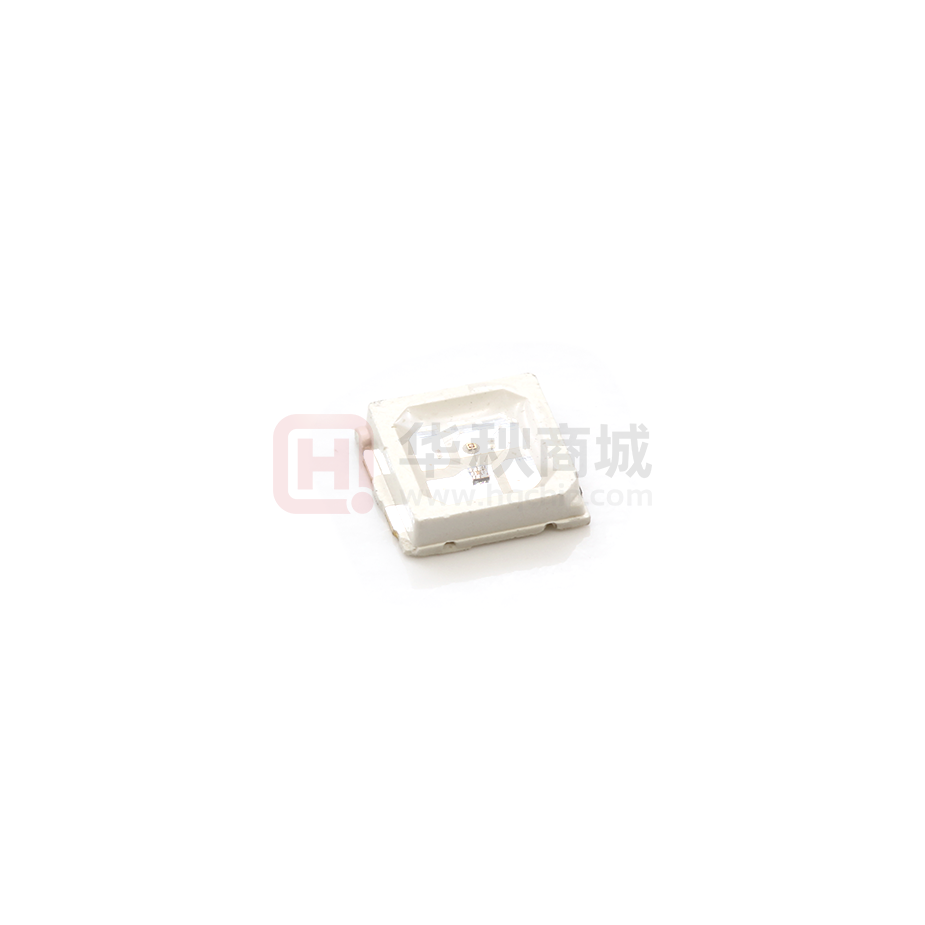
3535
haracteristics
* 外观尺寸(L/W/H):3.5*3.5*2.8 mm
Qutline Dimensions (L / w / h): 3.5*3.5*2.8 mm
* 发光颜色及胶体: 白色/黄色雾状
Luminous color and colloid: White/ Yellow mist
* 环保工艺符合ROHS要求
Environmental protection products Complied With ROHS Directive
* EIA规范标准包装
EIA standard packaging
* 适用于SMT贴片自动化生产
Suitable for SMT automatic production
* 适用于红外线回流焊制程
Suitable for infrared reflow soldering process
roduct application
* 医用设备:内窥镜、血氧仪
Medical equipment: endoscope、oximeter
* 汽车电子: 背光按键灯、指示灯
Automotive electronics: backlight key light、 indicator light
* 工业产品:电子仪表盘、工业设备
Industrial products: electronic instrument panel、industrial equipment
* 智能家居: 白色家电、数码管LED
Smart home: white appliances, nixie tube LED
* 通讯产品: 手机按键灯、路由器、电视盒
Communication products: mobile phone button lamp, router
1
�Catalogue
Electrical Characteristics...........................................................................................................................3
Typical Characteristic Curves...................................................................................................................8
Reliability Test Items And Conditions.......................................................................................................9
Outline Dimensions....................................................................................................................................10
Packaging......................................................................................................................................................11
Guideline for Soldering..............................................................................................................................13
Precautions....................................................................................................................................................15
2
�Electrical Characteristics
参数
Parameter
符号
Symbol
最小
Min
典型
Typical
最大
Max
测试条件
Test
conditions
单位
Unit
占空比 67%
数据传输速度
Data transmission speed
DOUT 传输延迟
Dout transmission delay
Iout 上升时间
IOUT rise time
fDIN
-
800
-
(数据 1)
KHZ
Duty
cycle
67% (data 1)
TPLH
-
-
500
ns
TPHL
-
-
500
ns
Tr
-
100
-
ns
Tr
-
100
-
ns
DIN→DOUT
VDS=1.5V
IOUT=13mA
电气参数(极限参数,Ta=25℃,VSS=0V) :
Absoiute Maximum Ratings (limit parameters, ta=25 ℃, vss=0v):
参 数
Parameters
电压
Voltage
符号
Symbol
范围
Range
Unit
VDD
+3.5~+5.5
V
逻辑输入电压
Logic input voltage
VI
-0.5~VDD+0.5
单位
V
工作温度
working temperature
Topt
-40~+85
℃
储存温度
Storage temperature
ESD耐压(设备模式)
ESDwithstand voltage
(device mode)
ESD耐压(人体模式)
ESDwithstand voltage
(human body mode)
Tstg
-50~+150
℃
VESD
200
VESD
4K
V
V
3
�IC电气参数(如无特殊说明,TA=-20~+70℃,VDD=4.5~5.5V,VSS=0V):
IC electrical parameters (unless otherwise specified, ta=-20 ~ +70 ℃, vdd=4.5 ~ 5.5V, vss=0v):
参数
Parameter
芯片内部电源电压
Chip internal power
supply voltage
单位
符号
Symbol
最小
Min
典型
Typical
最大
Max
Unit
测试条件
Test conditions
VDD
-
5.2
-
V
-
VDS,MAX
-
-
26
V
-
R/G/B端口耐压
R/g/b port withstand
voltage
IDOH
-
49
-
mA
IDOL
-
-50
-
mA
VIH
0.7*VDD
-
-
V
DOUT驱动能力
Dout drive capability
DOUT接地,最大
驱动电流
Dout grounding,
maximum drive
current
DOUT接正,最大
灌电流
Dout is connected
positively, and the
maximum perfusion
current
VDD=5.0V
信号输入翻转阀值
Signal input flip threshold
VIL
-
-
0.3*VDD
V
PWM频率
FPWM
-
1.2
-
KHZ
-
IDD
-
1
-
mA
-
PWM frequency
静态功耗
Static power consumption
0
4
�数据传输时间:
Data transmission time
时序表名称
Timeline name
T
T0H
码元周期
Symbol period
最小
Min
实际值
Actual value
最大
Max
1.20
--
--
µs
0.2
0.3
0.4
µs
0码, 高电平时间
0 code, high level time
单位
Unit
T0L
0码, 低电平时间
0 code, low level time
0.8
--
--
µs
T1H
1码, 高电平时间
1 code, high level time
0.58
0.64
1.0
µs
0.2
--
--
µs
>80
--
--
µs
T1L
Trst
1码, 低电平时间
1 code, low level time
Reset码,低电平时间
Reset code, low level time
◆ 协议采用单极性归零码,每个码元必须有低电平,本协议的每个码元起始为高电平,高电平时间宽度决定“0”
码或“1”码。
◆ 书写程序时,码元周期最低要求为 1.2µs。
◆ “0”码、 “1”码的高电平时间需按照上表的规定范围,
“0”码、 “1”码的低电平时间要求小于 20µs.
◆ the protocol adopts unipolar zeroing code, and each symbol must have a low level. Each symbol of the protocol starts with a
high level, and the time width of the high level determines the "0" code or "1" code.
◆ when writing the program, the minimum symbol period is 1.2 µ s.
◆ the high-level time of "0" code and "1" code shall be within the range specified in the above table, and the low-level time of
"0" code and "1" code shall be less than 20 µ s
数据传输方式(Ta=25℃):Data transmission mode(Ta=25℃):
注:其中 D1 为 MCU 端发送的数据,D2、D3、D4 为级联电路自动整形转发的数据。
Note: D1 is the data sent by MCU, and D2, D3 and D4 are the data automatically shaped and forwarded by cascade circuit.
0
6
�光电参数
(Ta=25℃):
Photoelectric parameters
参数
Parameter
颜色
Colour
(Ta=25℃):
符号
Symbol
最小
Min
典型
Typical
最大
Max
450
-
550
1300
-
1500
350
-
400
-
120
-
2.0
-
2.2
3.0
-
3.2
蓝Blue
3.0
-
3.2
红Red
620
-
625
520
-
525
460
-
470
红Red
光强
light intensity
绿Green
IV
蓝Blue
半光强视角
Halflight angle
-
2θ1/2
红Red
正向电压
Forward voltage
主波长
Dominantwavele
ngth
绿Green
绿Green
VF
λD
蓝Blue
单位
Unit
mcd
deg
V
nm
测试条Test
conditions
IF=12mA
IF=12mA
IF=12mA
IF=12mA
亮度分档:Brightness classification:
颜色
Colour
代码
Code
最小
Min
最大
Max
红Red
CV4
450
550
绿Green
S02
1300
1500
蓝Blue
C26
350
400
单位
Unit
测试条件
Test conditions
mcd
IF = 12mA
单位
Unit
测试条件
Test conditions
V
IF = 12mA
单位
Unit
测试条件
Test conditions
nm
IF = 12mA
电压分档:Voltage grading:
颜色
Colour
代码
Code
最小
Min
最大
Max
红Red
I2
2.0
2.2
绿Green
I7
3.0
3.2
蓝Blue
I7
3.0
3.2
色温分档:Color temperature grading:
颜色
Colour
代码
Code
最小
Min
最大
Max
红Red
R0
620
625
绿Green
G12
520
525
蓝Blue
PB12
460
470
1
6
�24bit 数据结构(Ta=25℃):24bit data structure (ta=25 ℃):
注:高位先发,按照 GRB 的顺序发送数据(G7 → G6 →… .. B0)
典型应用电路:
在实际应用电路中,为防止产品在测试时带电插拔产生的瞬间高压损伤IC内部信号输入输出引脚,应在信号输入及输出
端串接保护电阻。此外,为了使各IC芯片间更稳定工作,各灯珠间的退偶电容则必不可少;
应用一:用于软灯灯或硬灯条的,灯珠间传输距离短的,建议在信号及时钟线输入输出端
各串接保护电阻,即R1=R0 约 500 欧;
应用二:用于模组或一般异形产品,灯珠间传输距离长,因线材及传输距离不同,在信号及时钟线
两端串接的保护电阻会略有不同;以实际使用情况定;
In the practical application circuit, in order to prevent the instantaneous high voltage generated by the hot plug of
the product during the test from damaging the IC internal signal input and output pins, the protective resistors
should be connected in series at the signal input and output terminals. In addition, in order to make the IC chips
work more stably, the decoupling capacitor between the lamp beads is essential;
Application 1: it is used for soft light or hard light bar, and the transmission distance between light beads is short. It
is recommended to use it at the input and output end of the signal clock line
Each protective resistor is connected in series, that is, r1=r0 is about 500 Ω;
Application 2: for modules or general special-shaped products, the transmission distance between lamp beads is
long. Due to different wire and transmission distance, the protection resistance connected in series at both ends of
the signal clock line will be slightly different; Subject to actual use;
2
7
�Typical Characteristics Curves
注: 如无另外注明,测试环境温度为25 + 3C If not otherwise noted, the test ambient temperature is 25 + 3C .
0
8
�可靠性实验
Reliability experiment
实验项目
Experimental
items
序号
Serial number
1
2
3
4
5
冷热冲击
Thermal Shock
实验条件
Experimental condition
参考标准
Reference standard
100 ±5°C ~ -40°C ±5°C
30min~30min 300cycles
MIL-STD-202G
高温储藏
High temperature
storage
Ta= +100ºC
低温储藏
Low temperature
storage
Ta= -40ºC
高温高湿储藏
High temperature
and humidity
storage
Ta=60ºC
温度循环
Temperature cycle
判断
judge
0/22
JEITA ED-4701 200 201
1000hrs
JEITA ED-4701 200 202
1000hrs
JEITA ED-4701 100 103
RH=90% 1000hrs
0/22
0/22
0/22
-55ºC~25ºC~100ºC~25ºC
30min~5min~30min~5min 100 cycles
JEITA ED-4701 100 105
0/22
JEITA ED-4701 300 301
0/22
6
耐焊接热
Resistance to
welding heat
Tsld = 260°C, 10sec. 3 times
7
常温寿命测试
Normal
temperature life
test
25°C, IF: Typical current , 1000hrs
JESD22-A 108D
0/22
判断标准Judgment criteria
项目
project
符号
Symbol
测试条件
Test conditions
发光强度
Luminous intensity
IV
DC=5V,规格典型电流
Dc=5v, specification typical current
耐焊接热
Resistance to welding
heat
-
DC=5V,规格典型电流
Dc=5v, specification typical current
1
最小值
minimum value
最大值
Maximu
m value
初始数据X0.7
Initial data x0.7
---
无死灯或明显损坏
No dead light or obvious damage
9
�3535RGBC-WS2812B
Outline Dimension
备注: 1.单位:毫米(mm)
Remarks: 1 Unit: mm
2.公差: 如无特别标注则为±0.10mm
2. Tolerance: ± 0.10mm unless otherwise specified
10
�3535RGBC-WS2812B
1
Packaging (1)
Belt and disk dimensions
注:
1. 尺寸单位为毫米(mm)。
1. Size unit is mm (mm).
2. 尺寸公差是±0.1mm。
2. The dimensional tolerance is ± 0.1mm.
Disk and carrier belt direction of roll and hole dimensions
11
�2
Packaging (2)
12
�3535RGBC-WS2812B
1
Guideline for Soldering (1)
1.
Hand Soldering
只建议在修理和重工的情况下使用手工焊接;推荐使用功率低于 3 0 W 的烙铁,焊接时烙铁的温度必须保
持在 300℃以下,且每个电极只能进行一次焊接,每次焊接的持续时间不得超过 3 秒。
人手焊接过程中的不慎操作易引起 LED 产品的损坏,应当小心谨慎。
Manual welding is recommended only for repair and heavy industry situations. A soldering iron of less than 30W
is recommended to be used in Hand Soldering. Please keep the temperature of the soldering iron under 300℃ while
soldering. Each terminal of the LED is to go for less than 3 second and for one time only.
Be careful because the damage of the product is often started at the time of the hand soldering.
2.
推荐使用以下无铅回流焊接温度图进行。
Reflow Soldering: Use the conditions shown in the under Figure ofPb-Free Reflow Soldering.
有铅制程 have lead process
无铅制程 Lead-free process
· 回流焊接最多只能进行两次。
Reflow soldering should not be done more than two times.
· 在回流焊接升温过程中,请不要对 LED 施加任何压力。
Stress on the LEDs should be avoided during heating in soldering process.
· 在焊接完成后,待产品温度下降到室温之后,再进行其他处理。
After soldering, do not deal with the product before its temperature drop down to room temperature.
13
�3535RGBC-WS2812B
2
Guideline for Soldering (2)
3.
Cleaning
在焊接后推荐使用酒精进行清洗,在温度不高于 30℃的条件下持续 3 分钟, 不高于 50℃的条件下持续 30
秒。使用其他类似溶剂清洗前,请先确认使用的溶剂不会对 LED 的封装和环氧树脂部分造成损伤。
超声波清洗也是有效的方法,一般最大功率不应超过 300W ,否则可能对 LED 造成损伤。请根据具体的
情况预先测试清洗条件是否会对 LED 造成损伤。
It is recommended that alcohol be used as a solvent for cleaning after soldering. Cleaning is to go under 30℃ for
3 minutes or 50℃ for 30 seconds. When using other solvents, it should be confirmed beforehand whether the solvents
will dissolve the package and the resin or not.
Ultrasonic cleaning is also an effective way for cleaning. But the influence of Ultrasonic cleaning on LED
depends on factors such as ultrasonic power. Generally, the ultrasonic power should not be higher than 300W. Before
cleaning, a pretest should be done to confirm whether any damage to LEDs will occur.
此一般指导原则并不适用于所有 PCB 设计和焊接设备的配置。具体工艺受到诸多因素的影响,
请根据特定的PCB设计和焊接设备来确定焊接方案。
Note: This general guideline may not apply to all PCB designs and configurations of all soldering equipment.
The technics in practise is influenced by many factors, it should be specialized base on the PCB designs
and configurations of the soldering equipment..
14
�1
Precautions (1)
1.
Storage
· 本产品使用密封防潮抗静电袋包装,并附有干燥剂,未开封的产品有一年的保存时间。
Moisture proof and anti-electrostatic package with moisture absorbent material is used, to keep moisture to a
minimum.
· 开封前,产品须存放在温度不高于 30℃,湿度不高于 40%RH 的环境中。
Before opening the package, the product should be kept at 30℃ or less and humidity less than 4 0 % RH, and
be used within a year.
· 开封后,产品须存放在温度不高于 30℃,湿度不高于 10%RH 的环境中,且应该在 24小时(1天) 内使
用完;且贴片后应尽快做焊接。建议工作环境为温度不高于 30℃,湿度不高于 40%RH。
After opening the package, the product should be stored at 30℃ or less and humidity less than 10%RH, and be
soldered within 2 4 hours (1 day). An d it sh o u l d be we l d e d as so o n as po s s i b l e af t e r th e pa t c h . It is
recommended that the product be operated at the workshop condition of 30℃ or less and humidity less than
40%RH.
· 对于尚未焊接的 LED,如果吸湿剂或包装失效,或者产品没有符合以上有效存储条件,烘焙可以起到一定
的性能恢复效果。烘焙条件: (60±5)℃,持续 24 小时。
If the moisture absorbent material has fade away or the LEDs have exceeded the storage time, baking treatment
should be performed based on the following condition: (60±5)℃ for 24 hours.
2.
Static Electricity
静电和电涌会导致产品特性发生改变,例如正向电压降低等,如果情况严重甚至会损毁产品。所以在使用时必须
采取有效的防静电措施。
所有相关的设备和机器都应该正确接地,同时必须采取其他防止静电和电涌的措施。使用防静电手环,防静电
垫子,防静电工作服、工作鞋、手套,防静电容器,都是有效的防止静电和电涌的措施;严禁使用普通塑料制品。建
议在作业过程中,使用离子风扇来压制静电的产生。距离LED元件1英尺距离的环境范围内静电场电压小于100V。
Static electricity or surge voltage damages the LEDs. Damaged LEDs will show some unusual characteristic such
as the forward voltage becomes lower, or the LEDs do not light at the low current. even not light.
All devices, equipment and machinery must be properly grounded. At the same time, it is recommended that wrist
bands or anti-electrostatic gloves, anti-electrostatic containers be used when dealing with the LEDs.Using ordinary
plastic products are strictly prohibited.It is recommended to use ion fans to suppress the static electricity generation
during the operation.The static field voltage is less than 100V within the ambient range of 1 foot distance from the LED
element.
15
�2
Precautions (2)
3.
Design Consideration
设计电路时,通过 LED 的电流不能超过规定的最大值,同时,还需使用保护电阻,否则,微小的电压变
化将会引起较大的电流变化,可能导致产品损毁。
建议使用以下(A)电路,该电路能够很好的调节通过每个 LED 的电流; 不推荐使用(B)电路,该电路
在持续的电压驱动下,LED 的正向电压(VF )发生变化,电流会随之而发生变化,可能使某些 LED 承受高于
规定的电流值。
In designing a circuit, the current through each LED must not exceed the absolute maximum rating specified for
each LED. In the meanwhile, resistors for protection should be applied, otherwise slight voltage shift will cause big
current change, burn out may happen.
It is recommended to use Circuit A which regulates the current flowing through each LED rather than Circuit B.
When driving LEDs with a constant voltage in Circuit B, the current through the LEDs may vary due to the variation
in Forward Voltage (VF) of the LEDs. In the worst case, some LED may be subjected to stresses in excess of the
Absolute Maximum Rating.
(A)
(B)
光电参数公差:
正向电压REF / VF: + 0.1V
亮度CAT / IV:
+ 15%
波长HUE / WLD: + 1nm
LED 的特性容易因为自身的发热和环境的温度的改变而发生改变。温度的升高会降低 LED 的发光效率、
影响发光颜色等,所以在设计时应充分考虑散热的问题。
Thermal Design is paramount importance because heat generation may result in the Characteristics decline,
such as brightness decreased, Color changed and so on. Please consider the heat generation of the LEDs when
making the system design.
16
�3
Precautions (3)
4.
Others
直接用手拿取产品不但会污染封装树脂表面,也可能由于静电等因素导致产品性能的改变。过度的压力也可能
直接影响封装内部的管芯和金线,因此请勿对产品施加过度压力,特别当产品处于高温状态下,例如在回流焊接过
程中。
When handling the product, touching the encapsulant with bare hands will not only contaminate its surface, but
also affect on its optical characteristics. Excessive force to the encapsulant might result in catastrophic failure of the
LEDs due to die breakage or wire deformation. For this reason, please do not put excessive stress on LEDs, especially
when the LEDs are heated such as during Reflow Soldering.
LED 的环氧树脂封装部分相当脆弱,请勿用坚硬、尖锐的物体刮、擦封装树脂部分。在用镊子夹取的时
候也应当小心注意。
The epoxy resin of encapsulant is fragile, so please avoid scratch or friction over the epoxy resin surface. While
handling the product with tweezers, do not hold by the epoxy resin, be careful.
5.
Safety Advice For Human Eyes
LED 发光时,请勿直视发光光源,特别是对于一些光强较高的 LED ,强光可能伤害你的眼睛。
Viewing direct to the light emitting center of the LEDs, especially those of great Luminous Intensity, will cause
great hazard to human eyes. Please be careful.
17
�