旌芯半导体科技(上海)有限公司
GN Semiconductor (Shanghai) Co., Ltd.
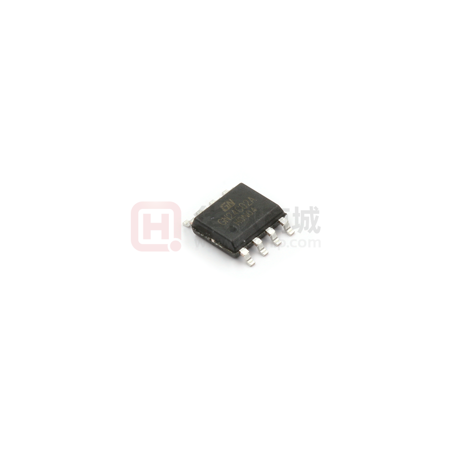
GN24C02A
I2C-Compatible Serial EEPROM
General Description
The GN24C02A is 2-Kbit I C-compatible Serial EEPROM (Electrically Erasable Programmable Memory)
2
device. It contains a memory array of 256 ×8bits, which is organized in 8 bytes per page. GN24C02A provides
the following devices for different application.
Device Selection Table
Max. Clock Frequency
Device Name
Voltage Range
Temp. Range
GN24C02A -LI
1.6V~5.5V
-40°C ~ 85°C
1MHz
GN24C02A -MI
1.7V~5.5V
-40°C ~ 85°C
1MHz
[1]
[1]
Note 1: 400 kHz for VCC < 2.5V.
Features
Single Supply Voltage and High Speed
Minimum operating voltage down to 1.6V
1 MHz clock from 2.5V to 5.5V
400kHz clock from 1.7V to 2.5V
Low power CMOS technology
Read current 400uA, maximum
Write current 1.6mA, maximum
Schmitt Trigger, Filtered Inputs for Noise Suppression
Sequential & Random Read Features
Page Write Modes, Partial Page Writes Allowed
Write protect of the whole memory array
Self-timed Write Cycle (5ms maximum)
High Reliability
Endurance: > 1 Million Write Cycles
Data Retention: > 100 Years
ESD HBM: 4KV
Latch-up Capability: +/- 200mA
Package: SOP8 SOT23-5 and TSOT23-5
中国(上海)自由贸易试验区芳春路400号1幢3层
http://www.gnsemic.com
电话:021-34125778
第 1 页,共 19页
�旌芯半导体科技(上海)有限公司
GN Semiconductor (Shanghai) Co., Ltd.
GN24C02A
1. Pin Configuration
1.1 Pin Configuration
Figure 1-1 Pin Configuration
E0
1
E1
2
8
VCC
7
WCB
GN24C02A
E2
3
6
SCL
GND
4
5
SDA
SCL
1
GND
2
SDA
3
5
WCB
4
Vcc
GN24C02A
1.2 Pin Definition
Table 1-1 Pin Definition
Pin
Name
Type
Description
1
E0
I/O
Slave Address Setting
2
E1
Input
Slave Address Setting
3
E2
Input
Slave Address Setting
4
GND
Ground
Ground
5
SDA
I/O
Serial Data Input and Serial Data Output
6
SCL
Input
Serial Clock Input
7
WCB
Input
Write Control, Low Enable Write
8
VCC
Power
Power
中国(上海)自由贸易试验区芳春路400号1幢3层
http://www.gnsemic.com
电话:021-34125778
第 2 页,共 19 页
�旌芯半导体科技(上海)有限公司
GN Semiconductor (Shanghai) Co., Ltd.
GN24C02A
1.3 Pin Descriptions
Serial Clock (SCL): The SCL input is used to positive-edge clock data in and negative-edge clock data out of
each device.
Serial Data (SDA): The SDA pin is bidirectional for serial data transfer. This pin is open drain driven and may
be wire-ORed with any number of other open-drain or open-collector devices.
Device Addresses (E2, E1, E0): The E2, E1 and E0 pins are device address inputs. Typically, the E2, E1
and E0 pins are for hardware addressing and a total of 8 devices can be connected on a single bus system. If
these pins are left floating, the E2, E1 and E0 pins will be internally pulled down to GND.
Write Control (WCB): The Write Control input, when WCB is connected directly to VCC, all write operations to
the memory are inhibited. When connected to GND, allows normal write operations. If the pin is left floating,
the WCB pin will be internally pulled down to GND.
2. Block Diagram
Figure 2-1 Block Diagram
SCL
SDA
Start Stop Control
Logic
NC
Slave Address
Comparator
High Voltage Generator
Serial Bus
Control Logic
Page Data Latch
MATCH
I
N
C
L
O
A
D
Address Counter
E1
X -DECODER
WCB
Write Control
Logic
EN
EEPROM ARRAY
E2
DataOut/ACK
Serial MUX
VCC
GND
Y-DECODER
中国(上海)自由贸易试验区芳春路400号1幢3层
http://www.gnsemic.com
电话:021-34125778
第 3 页,共 19 页
�旌芯半导体科技(上海)有限公司
GN Semiconductor (Shanghai) Co., Ltd.
GN24C02A
3. Electrical Characteristics
Absolute Maximum Ratings
NOTICE: Stresses above those listed under “Absolute
Storage Temperature .......................-65°C to +150°C
Operation Temperature ....................-40°C to +85°C
Maximum Operation Voltage............. 6.25V
Voltage on Any Pin with
Maximum Ratings” may cause permanent damage to the
device. This is a stress rating only and functional operation of
the device at those or any other conditions above those
indicated in the operational listings of this specification is not
Respect to Ground. ..........................-1.0V to (Vcc+1.0) V
implied. Exposure to maximum rating conditions for extended
DC Output Current ............................5.0 mA
Table 3-1 Pin Capacitance
Symbol
periods may affect device reliability.
[1]
Parameter
Max.
Units
Test Condition
CI/O
Input / Output Capacitance (SDA)
8
pF
VI/O=GND
CIN
Input Capacitance (E0, E1,E2,WCB,SCL)
6
pF
VIN=GND
Note: [1] Test Conditions: TA = 25°C, F = 1MHz, Vcc = 5.0V.
Table 3-2 DC Characteristics(Unless otherwise specified, VCC = 1.7V to 5.5V, TA = –40°C to 85°C)
Symbol
Parameter
Min.
Typ.
Max.
Unit
Test Condition
1.6
-
5.5
V
GN24C02A-LI
1.7
-
5.5
V
GN24C02A-MI
-
-
1.0
uA
Vcc = 3.3V, TA = 85°C
-
-
3.0
uA
Vcc = 5.5V, TA = 85°C
Isb
Standby Current
ICC1
Supply Current
-
0.2
0.4
mA
ICC2
Supply Current
-
0.8
1.6
mA
ILI
Input Leakage Current
-
0.10
1.0
µA
VIN = VCC or GND
ILO
Output Leakage Current
-
0.05
1.0
µA
VOUT = VCC or GND
VIL
Input Low Level
–0.6
-
0.3VCC
V
VIH
Input High Level
0.7VCC
-
VCC+0.5
V
-
-
0.2
V
IOL = 1.5 mA
-
-
0.4
V
IOL = 2.1 mA
VOL1
VOL2
Output Low Level
VCC = 1.7V (SDA)
Output Low Level
VCC = 3.0V (SDA)
中国(上海)自由贸易试验区芳春路400号1幢3层
http://www.gnsemic.com
电话:021-34125778
Vcc=5.5V,
Read at 400Khz
Vcc=5.5V
Write at 400Khz
第 4 页,共 19 页
�旌芯半导体科技(上海)有限公司
GN Semiconductor (Shanghai) Co., Ltd.
GN24C02A
Table 3-3 AC Characteristics
(Unless otherwise specified, VCC = 1.7V to 5.5V, TA = –40°C to 85°C, CL=100pF, Test Conditions are listed in Notes [2])
Symbol
1.7≤VCC
很抱歉,暂时无法提供与“GN24C02A”相匹配的价格&库存,您可以联系我们找货
免费人工找货- 国内价格
- 10+0.41635
- 100+0.34125
- 300+0.30370
- 1000+0.27548
- 4000+0.25076
- 8000+0.23947
- 国内价格
- 10+0.39768
- 100+0.32595
- 300+0.29008
