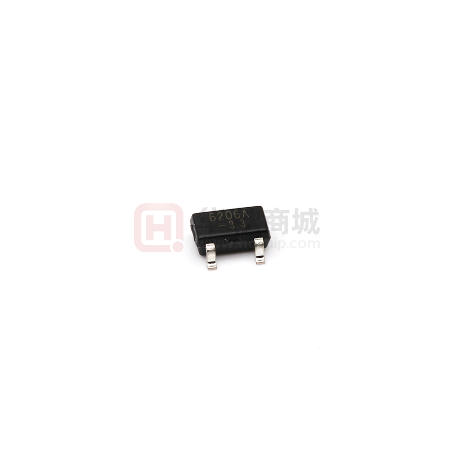
PJ6206A Series
Low Dropout Regulators
Description
SOT-23
3.VIN
The PJ6206A Series are highly precise, low power consumption, 3 terminal,
positive voltage regulators manufactured using CMOS technologies.
The PJ6206A Series consists of a current limiter circuit, a driver transistor, a
precision reference voltage and an error correction circuit. The series is
compatible with low ESR ceramic capacitors. The current limiter's foldback
circuit operates as a short circuit protection as well as the output current
1.GND
2.VOUT
SOT-23-3
3.VIN
limiter for the output pin.
Features
⚫ Quiescent Current: 8μA
⚫ Input Voltage Range: Max.6V
⚫ Output Current: 300mA
⚫ Low Dropout Voltage: 290mV@100mA (VOUT=3.3V)
⚫ Output Voltage: 1.2~5.0V
⚫ Output Voltage Accuracy: ±2%(Typ.)
1.GND
2.VOUT
SOT-89
2.VIN
⚫ Low Power Consumption
Applications
⚫ Battery-Powered Equipment
1.GND 2.VIN 3.VOUT
⚫ Mobile Phones
⚫ Portable game consoles
⚫ Reference voltage sources
Marking Code
6206A
-XX
XX:Output Voltage
e.g. 12:1.2V 50:5.0V
www.pingjingsemi.com
Revision:2.0 Sep-2021
1/8
PJ6206A Series
Low Dropout Regulators
Functional Pin Description
Pin Name
Pin Function
GND
Ground
VOUT
Output Voltage
VIN
Power Input Voltage
Ordering Information
PJ6206A-
Package Type
SA : SOT-23
SC : SOT-23-3
SQ : SOT-89
Output Voltage
12 : 1.2V 15 : 1.5V 18 : 1.8V
25 : 2.5V 28 : 2.8V 30 : 3.0V
33 : 3.3V 50 : 5.0V
Output current tap
L : 300mA
Version Number
Typical Application Circuit
www.pingjingsemi.com
Revision:2.0 Sep-2021
2/8
PJ6206A Series
Low Dropout Regulators
Function Block Diagram
VIN
VOUT
Current
Limited
Voltage
Reference
GND
www.pingjingsemi.com
Revision:2.0 Sep-2021
3/8
PJ6206A Series
Low Dropout Regulators
Absolute Maximum Ratings
Ratings at 25℃ ambient temperature unless otherwise specified.
Parameter
Input Voltage
VIN
Value
Unit
-0.3 ~ +6
V
Output Voltage
VOUT
-0.3~VIN+0.3
V
Output Current
IOUT
300
mA
SOT-23
200
mW
SOT-89
500
mW
SOT-23-3
250
mW
Operating Temperature Range
-20 ~ +85
°C
Storage temperature range
-55 ~ +125
°C
Power Dissipation
Electrical Characteristics
(VIN=VOUT+1, CIN=COUT=1µF, TA=25℃ , unless otherwise noted.)
Parameter
Input Voltage
Output Voltage Accuracy
Quiescent Current
Dropout Voltage Note1
Symbol
Test Conditions
VIN
Min.
Typ.
Max.
Unit
--
--
6
V
∆VOUT
IOUT=30mA
-2
--
+2
%
IQ
IOUT=0mA
--
8
15
μA
IOUT=100mA,VOUT≤1.5V
--
--
570
IOUT=100mA,1.8V≤VOUT≤2.5V
--
--
420
IOUT=100mA,2.8V≤VOUT≤5V
--
--
350
VDROP
mV
Line Regulation
∆VLINE
VIN=VOUT+1 to 6V,IOUT=40mA
--
--
0.2
%/V
Load Regulation
∆VLOAD
1mA
很抱歉,暂时无法提供与“PJ6206AL33SC”相匹配的价格&库存,您可以联系我们找货
免费人工找货- 国内价格
- 5+0.18020
- 20+0.16430
- 100+0.14840
- 500+0.13250
- 1000+0.12508
- 2000+0.11978