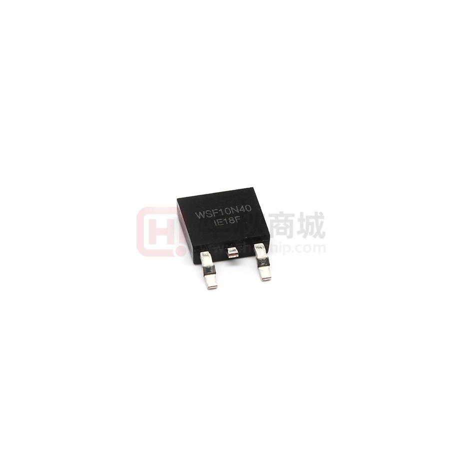
WSF10N40
N-Ch MOSFET
General Description
Product Summery
The WSF10N40 is the highest performance
trench N-Ch MOSFET with extreme high cell
density , which provide excellent RDSON and
gate charge for most of the synchronous buck
converter applications .
BVDSS
RDSON
ID
400V
515mΩ
10A
Applications
• DC-DC & DC-AC Converters for telecom,
industrial and consumer environment
• Uninterruptible Power Supply (UPS)
• Switch Mode Low Power Supplies
Features
• Industrial Actuators
TO-252 Pin Configuration
• Fast switching
• 100% avalanche tested
• Improved dv/dt capability
Absolute Maximum Ratings
Symbol
Parameter
VDS
VGS
ID@TC=25℃
ID@TC=100℃
ID@TA=25℃
ID@TA=70℃
IDM
Rating
Units
Drain-Source Voltage
400
V
Gate-Source Voltage
±25
V
1
10.0
A
1
5.6
A
1
1.2
A
1
0.6
A
36
A
Continuous Drain Current, VGS @ 10V
Continuous Drain Current, VGS @ 10V
Continuous Drain Current, VGS @ 10V
Continuous Drain Current, VGS @ 10V
Pulsed Drain Current
2
3
EAS
Single Pulse Avalanche Energy
220
mJ
IAS
Avalanche Current
27
A
4
56.0
W
4
PD@TC=25℃
Total Power Dissipation
PD@TA=25℃
Total Power Dissipation
1.5
W
TSTG
Storage Temperature Range
-55 to 150
℃
TJ
Operating Junction Temperature Range
-55 to 150
℃
Thermal Data
Symbol
Parameter
RθJA
Thermal Resistance Junction-ambient
RθJC
1
www.winsok.tw
Thermal Resistance Junction-Case
Page 1
1
Typ.
Max.
Unit
---
62
2.1
℃/W
---
℃/W
Rev 2: Apr.2019
�WSF10N40
N-Ch MOSFET
Electrical Characteristics (TJ=25 ℃, unless otherwise noted)
Symbol
BVDSS
Parameter
Conditions
Drain-Source Breakdown Voltage
△BVDSS/△TJ BVDSS Temperature Coefficient
RDS(ON)
VGS(th)
VGS=0V , ID=250uA
Reference to 25℃, ID = 250uA
Min.
Typ.
Max.
Unit
400
---
---
V
---
V/℃
---
0.3
=
=
VGS 10V,ID 4.5A
Static Drain-Source On-Resistance2
VGS=8.0V , ID=3A
---
515
607
---
1100
2000
Gate Threshold Voltage
2.0
---
4.0
V
---
-5.52
---
mV/℃
VDS=320V , VGS=0V , TJ=25℃
---
---
10
VDS=320V , VGS=0V , TJ=55℃
---
---
100
VGS=VDS , ID =250uA
mΩ
△VGS(th)
VGS(th) Temperature Coefficient
IDSS
Drain-Source Leakage Current
IGSS
Gate-Source Leakage Current
VGS=±20V , VDS=0V
---
---
±100
nA
gfs
Forward Transconductance
VDS=30V , ID=4.5A
---
8.0
---
S
Rg
Gate Resistance
VDS=0V , VGS=0V , f=1MHz
---
1.6
3.2
Ω
Qg
Total Gate Charge (10V)
---
25
35
Qgs
Gate-Source Charge
---
4.0
6.0
Qgd
Gate-Drain Charge
---
10.5
12.1
Turn-On Delay Time
---
12.4
---
Td(on)
VDS=320V , VGS=10V , ID=9A
uA
nC
Rise Time
VDD=200V , VGS=10V , RG=5Ω
---
20.1
---
Turn-Off Delay Time
ID=9A
---
38.5
---
Fall Time
---
10.8
---
Ciss
Input Capacitance
---
740
---
Coss
Output Capacitance
---
83
---
Crss
Reverse Transfer Capacitance
---
9.0
---
Min.
Typ.
Max.
Unit
100
---
---
mJ
Min.
Typ.
Max.
Unit
---
---
9.0
A
Tr
Td(off)
Tf
VDS=25V , VGS=0V , f=1MHz
ns
pF
Guaranteed Avalanche Characteristics
Symbol
EAS
Parameter
Conditions
5
Single Pulse Avalanche Energy
VDD=25V , L=0.1mH , IAS=10A
Diode Characteristics
Symbol
IS
Parameter
Conditions
1,6
Continuous Source Current
2,6
ISM
Pulsed Source Current
VSD
Diode Forward Voltage2
trr
Reverse Recovery Time
Qrr
Reverse Recovery Charge
VG=VD=0V , Force Current
VGS=0V , IS=4.5A
IF=9A , dI/dt=100A/µs
---
---
35
A
---
---
1.5
V
---
320
---
nS
---
1345
---
nC
Note :
1.The data tested by surface mounted on a 1 inch2 FR-4 board with 2OZ copper,t
很抱歉,暂时无法提供与“WSF10N40”相匹配的价格&库存,您可以联系我们找货
免费人工找货- 国内价格
- 1+2.41373
- 10+2.27173
- 30+1.98773
- 100+1.77473
- 500+1.63273
- 1000+1.53333
- 国内价格
- 1+2.19672
- 10+1.93428
- 30+1.81764
- 100+1.67184
- 500+1.61352
- 1000+1.57464