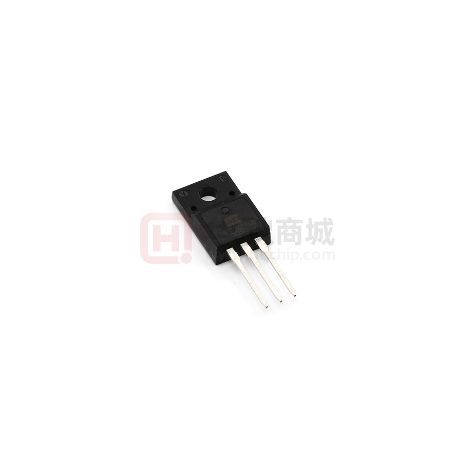
HFF20N65
650V N-Channel MOSFETs
withstand high energy pulse in the avalanche and
Features
650V,20A, RDS(ON) =0.35Ω@VGS = 10V
Improved dv/dt capability
Fast switching
100% EAS Guaranteed
Green Device Available
commutation mode. These devices are well suited
for high efficiency fast switching applications.
Product Summary
Applications
Networking
Load Switch
LED applications
Quick Charger
General Description
These N-Channel enhancement mode power field
effect transistors are using trench DMOS
BVDSS
650V
technology. This advanced technology has been
RDSON
0.35ohm
ID
20A
especially tailored to minimize on-state resistance,
provide superior switching performance, and
Absolute Maximum Ratings Tc =25℃ unless otherwise noted
Parameter
Symbol
Rating
Unit
Drain-Source Voltage
VDS
650
V
Gate-Source Voltage
VGS
±30
V
ID@Tc=25℃
20
A
ID@Tc=100℃
12.5
A
IDM
80
A
Single Pulse Avalanche Energy
EAS
1300
mJ
Single Pulse Avalanche Current
IAS
20
A
Power Dissipation-
Derate above 25℃
0.31
W/℃
Power Dissipation
TC=25℃
45
TJ
-55 to 150
W
℃
TSTG
-55 to 150
℃
Continuous Drain Current
Pulsed Drain Current
Operating Junction Temperature
Storage Temperature
Thermal Resistance
Parameter
Symbol
Min.
Typ.
Max.
Unit
Thermal resistance, junction - case
RthJC
---
---
2.6
℃/W
Thermal Resistance Junction to ambient
RthJA
---
---
65
℃/W
Soldering temperature, wave soldering for 10s
Tsold
---
---
265
℃
1
�HFF20N65
650V N-Channel MOSFETs
Electronic Characteristics TJ =25℃ unless otherwise noted
Off Characteristics
Parameter
Condition
Drain-Source Breakdown Voltage
VGS =0V, ID =250uA
Drain-Source Leakage Current
Gate- Source Leakage Current
Symbol
Min.
Typ.
Max.
Unit
BVDSS
650
700
---
V
---
---
1
---
---
10
IGSS
---
---
±100
nA
Symbol
Min.
Typ.
Max.
Unit
VDS=650V, VGS =0V
IDSS
VDS=520V, VGS =0V
VGS=±30V, VDS =0V
uA
On Characteristics
Parameter
Condition
Static Drain-source On Resistance
VGS=10V, ID=5A
RDS(ON)
---
0.3
0.35
Ω
Gate Threshold Voltage
VGS =VDS, ID=250uA
2.0
3.0
4.0
V
Forward Transconductance
VDS =40V, ID=10A
VGS(TH)
gFS
---
3.4
---
S
Symbol
Min.
Typ.
Max.
Unit
Dynamic and switching Characteristics
Parameter
Condition
Total Gate Charge
VDS=400V
Qg
---
58
---
Gate-Source Charge
VGS=10V
Qgs
---
13
---
Gate-Drain Charge
ID=20A
Qgd
---
23
---
Turn-On Delay Time
VDD=250V
Td(on)
---
36
---
Rise Time
VGS=10V
Tr
---
74
---
Turn-Off Delay Time
RG=10Ω
Td(off)
---
78
---
Fall Time
ID=20A
Tf
---
58
---
Input capacitance
VDS=25V
Ciss
---
2900
---
Output capacitance
VGS=0V
Coss
---
310
---
Reverse transfer capacitance
F=1MHz
Crss
---
20
---
Gate resistance
VDS=0V,VGS=0V,F=1MHz
Rg
---
2.5
---
Ω
Symbol
Min.
Typ.
Max.
Unit
nC
ns
F
P
Drain-Source Diode Characteristics and Maximum Ratings
Parameter
Condition
Diode Forward Voltage
VGS=0V,IS=10A
VSD
---
0.7
1.4
V
Reverse Recovery Time
IF=10A, dI/dt=40A/μs,
VDS=100V
trr
---
491
---
nS
Qrr
---
2296
---
nC
Reverse Recovery Charge
Note:
1. Repetitive Rating: Pulsed width limited by maximum junction temperature.
2. VDD=650V, VGS=10V, L=1mH,IAS=10A.,RG=25 ,Starting TJ=25℃.
3. The data tested by pulsed, pulse width ≦ 300us, duty cycle ≦ 2%.
4. Essentially independent of operating temperature.
2
�HFF20N65
650V N-Channel MOSFETs
Figure 1 Maximum Forward Bias Safe Operating Area
Figure 2 Maximum Power dissipation vs Case Temperature
Figure 4 Typical Output Characteristics
Figure 3 Maximum Continuous Drain Current vs Case Temperature
Figure 4 Typical Output Characteristics
Figure 5 Maximum Effective Thermal Impedance , Junction to Case
3
�HFF20N65
650V N-Channel MOSFETs
Figure 6
Figure 7 Typical Body Diode Transfer Characteristics
TypicalTransfer Characteristics
Figure 8 Typical Capacitance vs Drain to Source Voltage
4
Figure 9 Typical Gate Charge vs Gate to Source Voltage
�HFF20N65
650V N-Channel MOSFETs
TO-220F PACKAGE INFORMATION
Symbol
Dimensions In Millimeters
Dimensions In Inches
MAX
MIN
MAX
MIN
A
10.460
9.860
0.412
0.388
A1
7.100
6.900
0.280
0.272
A2
3.500
3.100
0.138
0.122
A3
9.900
9.500
0.390
0.374
B1
16.170
15.570
0.637
0.613
B2
4.900
4.500
0.193
0.177
B3
6.880
6.480
0.271
0.255
C
3.500
3.100
0.138
0.122
C1
12.870
12.270
0.507
0.483
C2
13.380
12.580
0.527
0.495
D
2.590
2.490
0.102
0.098
D1
1.470
1.070
0.058
0.042
D2
0.900
0.700
0.035
0.028
E1
2.740
2.340
0.108
0.092
E3
0.600
0.400
0.024
0.016
E4
2.960
2.560
0.117
0.101
DIA
Φ1.5 TYP.
deep0.1 TYP.
Φ0.059 TYP.
deep0.004 TYP.
5
�
很抱歉,暂时无法提供与“HFF20N65”相匹配的价格&库存,您可以联系我们找货
免费人工找货