MMBT5551
2N7002
AO3400
SI2305
2N7002
N-Channel Enhancement Mode Field Effect Transistor
Description
These N-channel enhancement mode field effect transis-tors
are produced using ON Semiconductor's proprietary, high cell
density, DMOS technology.These products have been designed to
minimize on-state resistance while providing rugged, reliable, and
fast switching performance.They can be used in most applications
requiring up to 400 mA DC and can deliver pulsed currents up to 2
A. These products are particularly suited for low-voltage, low-current applications, such as small servo motor control, power
MOSFET gate drivers, and other switching appli-cations.
SOT-23
D
2. SOURCE
3. DRAIN
MARKING: 7002
G
S
Features
•
•
•
•
1. GATE
High Density Cell Design for Low RDS(ON)
Voltage Controlled Small Signal Switch
Rugged and Reliable
High Saturation Current Capability
Absolute Maximum Ratings
Symbol
Parameter
Value
Unit
VDSS
Drain-to-Source Voltage
60
V
VDGR
VGSS
Drain-Gate Voltage (RGS ≤ 1 MΩ )
Gate-Source Voltage - Continuous
60
±20
±40
V
V
115
800
200
mA
mW
1.6
-55 to 150
300
mW/°C
°C
°C
ID
PD
TJ, TSTG
TL
Gate-Source Voltage - Non Repetitive (tp < 50 S)
Maximum Drain Current - Continuous
Maximum Drain Current - Pulsed
Maximum Power Dissipation Derated above 25°C
Operating and Storage Temperature Range
Maximum Lead Temperature for Soldering Purposes, 1/16inch from Case for 10 Seconds
Thermal Characteristics
Values are at TC = 25°C unless otherwise noted.
Parameter
RJA
www.tw-gmc.com
Thermal Resistance, Junction to Ambient
1
Value
Unit
625
°C/W
�MMBT5551
2N7002
AO3400
SI2305
Electrical Characteristics
Values are at TC = 25°C unless otherwise noted.
Symbol
Parameter
Off Characteristics
Conditions
BVDSS
Drain-Source Breakdown Voltage VGS = 0 V, ID = 10 A
IDSS
Zero Gate Voltage Drain Current VDS = 60 V, VGS = 0 V
Min.
Typ.
Max.
60
Unit
V
1
A
VDS = 60 V, VGS = 0 V, TC =
125°C
0.5
mA
IGSSF
Gate - Body Leakage, Forward
VGS = 20 V, VDS = 0 V
100
nA
IGSSR
Gate - Body Leakage, Reverse
VGS = -20 V, VDS = 0 V
-100
nA
Electrical Characteristics (Continued)
Symbol
Parameter
On Characteristics
Conditions
VGS(th)
Gate Threshold Voltage
VDS = VGS, ID = 250 A
RDS(ON)
Static Drain-Source OnResistance
VDS(ON)
Drain-Source On-Voltage
ID(ON)
On-State Drain Current
gFS
Forward Transconductance
Min.
Typ.
Max.
Unit
2.1
2.5
V
VGS = 10 V, ID = 500 mA
1.2
7.5
VGS = 10 V,
ID = 500 mA, TC = 100°C
1.7
13.5
VGS = 10 V,
ID = 500 mA
0.6
3.75
VGS = 5.0 V, ID = 50 mA
0.09
1.5
VGS = 10 V, VDS 2 VDS(on)
VDS 2VDS(ON), ID = 200 mA
1
V
500
2700
mA
80
320
mS
Dynamic Characteristics
Ciss
Coss
Input Capacitance
Output Capacitance
Crss
Reverse Transfer Capacitance
ton
Turn-On Time
toff
VDS = 25 V, VGS = 0 V, f =
1.0 MHz
20
11
50
25
4
5
pF
VDD = 30 V, RL = 150Ω ID =
200 mA, VGS= 10 V, RGEN
= 25Ω
20
ns
Turn-Off Time
VDD = 30 V, RL = 150 ID =
200 mA, VGS= 10 V, RGEN
= 25Ω
Drain-Source Diode Characteristics and Maximum Ratings
20
ns
IS
Maximum Continuous Drain-Source Diode Forward Current
115
mA
ISM
Maximum Pulsed Drain-Source Diode Forward Current
0.8
A
VSD
Drain-Source Diode
Forward Voltage
1.2
V
VGS = 0 V,
IS = 400 mA(1)
Note:
1. Pulse test : Pulse Width ≤ 300 μs, Duty Cycel ≤ 2 %.
www.tw-gmc.com
1
2
0.88
�MMBT5551
2N7002
AO3400
SI2305
Typical Characteristics
3
9.0
8.0
1 .5
RDS(on) , NORMALIZED
DRAIN-SOURCE ON-RESISTANCE
VGS = 10V
7.0
6.0
1
5.0
0 .5
4.0
V GS =4.0V
4 .5
5 .0
2 .5
6 .0
2
7 .0
8 .0
1 .5
9 .0
10
1
I
D
, DRAIN-SOURCE CURRENT (A)
2
3.0
0
1
2
3
V DS , DRAIN-SOURCE VOLTAGE (V
4
0 .5
5
0 .8
1 .2
I D , DRA IN CURRENT (A)
1 .6
2
2
3
V GS = 10V
RDS(on) , NORMALIZED
I D = 500m A
1.5
1.25
1
0.75
V GS
2 .5
TJ = 1 2 5 ° C
2
1 .5
25°C
1
-55°C
0 .5
0.5
-5 0
-2 5
0
25
50
75
100
TJ , JUNCTION T EMPERATURE (°C)
125
0
150
Figure 3. On-Resistance Variation
with Temperature
0
0 .4
0 .8
1 .2
I D , DRAIN CURRENT (A)
1 .6
2
Figure 4. On-Resistance Variation with Drain
Current and Temperature
2
T J = -55°C
25°C
1.6
Vth , N250$/,=(D
WK9�����1250$/,=('
*$7(�6285&(�7+5(6+2/'�92/7$*(
1 .1
VDS = 10 V
,����
D , DRAIN CURRENT (A)
0 .4
Figure 2. On-Resistance Variation with Gate
Voltage and Drain Current
1.75
125°C
1.2
0.8
0.4
0
0
Figure 1. On-Region Characteristics
DRAIN-SOURCE ON-RESISTANCE
RDS(on) , NORMALIZED
DRAIN-SOURCE ON-RESISTANCE
0
0
2
V
GS
4
6
8
, GATE TO SOURCE VOLTAGE (V
Figure 5. Transfer Characteristics
www.tw-gmc.com
I D = 1 mA
1
0 .9 5
0 .9
0 .8 5
0 .8
-50
10
V DS = VGS
1 .0 5
-25
0
25
50
75
100
TJ , JUNCTION TEM PERATURE (°C)
Figure 6. Gate Threshold Variation with
Temperature
1
3
125
150
�MMBT5551
2N7002
AO3400
SI2305
Typical Characteristics
2
I D = 250µA
1.05
1.025
1
0.975
0.95
0.925
-50
-25
0
25
50
75
100
TJ , JUNCTION TEM PERATURE (°C)
125
150
0 .5
25°C
0 .0 5
-5 5 ° C
0 .0 1
0 .0 0 5
0 .0 0 1
0 .2
0 .4
V SD
0 .6
0 .8
1
1 .2
, BODY DIODE FORW A RD VOLTAGE (V)
1 .4
10
60
V DS = 2 5 V
VGS , GA E-SOURCE VOLTAGE (V)
40
C iss
CAPACITANCE (pF)
TJ = 1 2 5 ° C
0 .1
Figure 8. Body Diode Forward Voltage Variation with
Figure 7. Breakdown Voltage Variation
with Temperature
20
C oss
10
5
C rss
f = 1 MHz
2
1
V GS = 0V
1
IS , REVERSE DRAIN CURRENT (A)
BVDSS , NORMALIZED
DRAIN-SOURCE BREAKDOWN VOLTAGE
1.1
1.075
V GS = 0V
1
2
VDS
3
5
10
20
, DRAIN TO SOURCE VOLTAGE (V)
30
8
6
I D =5 0 0 m A
4
2
0
50
Figure 9. Capacitance Characteristics
280m A
0
0 .4
0 .8
t on
t d(on)
R GEN
V OUT
Output, Vout
tf
90%
10%
10%
90%
DUT
G
2
t off
t d(off)
90%
Input, Vin
50%
50%
10%
S
Pulse Width
Figure 11.�6ZLWFKLQJ�7HVW�&LUFXLW
www.tw-gmc.com
tr
RL
D
VGS
1 .6
1 .2
Figure 10. Gate Charge Characteristics
VDD
V IN
0 .8
1 .2
Q g , GATE CHARGE (nC)
115m A
Figure 12. Switching Waveforms
1
4
Inverted
�MMBT5551
2N7002
AO3400
SI2305
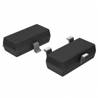
PACKAGE OUTLINE
Plastic surface mounted package; 3 leads
www.tw-gmc.com
SOT-23
1
5
�