WPM1480
WPM1480
Http://www.sh-willsemi.com
Single P-Channel, -20 V, -1.5 A,Power Mosfet
Description
3
The WPM1480 uses advanced trench technology and design to
provide excellent RDS(ON) with low gate charge. This device is
suitable for use in DC-DC conversion applications. Standard
Product WPM1480 is Pb-free.
1
2
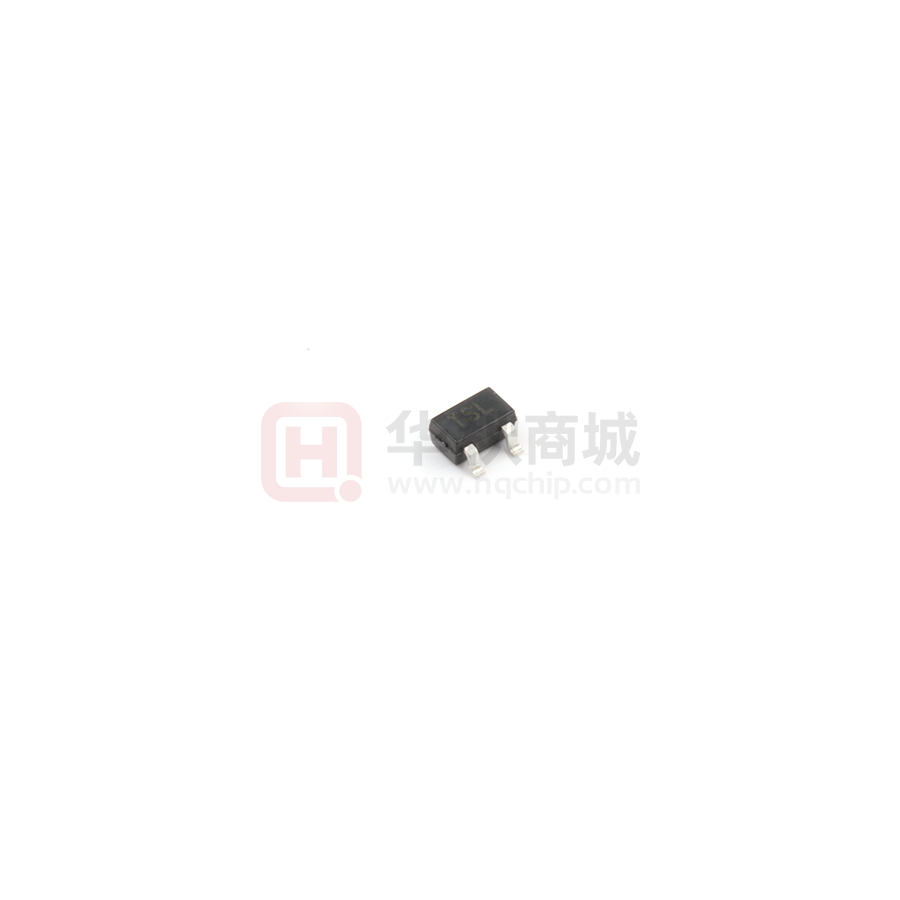
SC−70/SOT−323
Features
9�%5�'66�
�20 V
5'6�RQ��7\S�
110 m¡ @ �4.5 V
150 m¡ @ �2.5 V
P−Channel MOSFET
S
Application
G
z
Li-Ion Battery Charging
z
High Side DC-DC Conversion Circuits
z
High Side Drive for Small Brushless DC Motors
z
Power Management in Portable, Battery Powered Products
D
Absolute Maximum Ratings (TA=25 unless otherwise specified)
3DUDPHWHU�
6\PERO�
VDS
Drain-Source voltage
VGS
Gate-Source Voltage
Steady-State TA=25ć
ID
Continuous
Drain
Steady-State TA=70ć
CurrentA
TA=25ć
t ̰5s
IDM
Pulse Drain Current B
Tp=10us
PD
Power Dissipation B
TA=25ć
TA=70ć
TJ
Operating Junction Temperature Range
Tstg
Storage Temperature Range
9DOXH 8QLWV
-20
V
±8
V
-1.4
A
-1.1
-1.5
-3.0
A
0.29
W
0.19
-55~150 ć
Drain
3
TS M
2
1
Gate
Source
TS = Specific Device Code
M= Date Code
Order information
3DUW�1XPEHU�
WPM1480-3/TR
Will Semiconductor Ltd.
3DUW�1XPEHU�
SOT-323/SC-70
1
6KLSSLQJ�
3000Tape&Reel
2015/08/25 – Rev. 1.4
�WPM1480
Electrical Characteristics
OFF
Symbol
BVDSS
Parameter
Drain-Source Voltage
Test conditions
ID=-250�A, VGS=0V
IDSS
Zero Gate Voltage Drain Current
IGSS
Gate-body Leakage Current
VDS=0V, VGS=f8V
Min. Typ. Max. Units
-20
V
-1
�A
-5
�A
±100 nA
Parameter
Gate Threshold Voltage
Test conditions
VDS=VGS, ID=-250A
VGS= -4.5V, ID= -1.0A
VGS= -2.5V, ID= -0.5A
VGS= -1.8V, ID= -0.3A
Min. Typ. Max. Units
-0.4 -0.6 -1.0
V
110 255 m �
150 355 m �
190 405 m �
VDS= -16V, VGS=0V
TC=25ć
TC=55ć
ON
Symbol
VGS(th)
RDS(ON) Static Drain-Source On resistance
Dynamic
Symbol
gFS
Ciss
Coss
Crss
Rg
Parameter
Transconductance
Input Capacitance
Output Capacitance
Reverse Transfer Capacitance
Gate Resistance
Test conditions
VDS= -10V, ID = -1A
VDS=0V, VGS=0V, f=1MHz
Min. Typ. Max. Units
4
6
S
480
pF
58
pF
pF
51
12
�
Test conditions
Min. Typ. Max. Units
VDS= -10V, VGS=0V, f=1MHz
Switching
Symbol
Parameter
Qg
Total Gate Charge
Qgs
Gate Source Charge
Qgd
Gate Drain Charge
tD(on)
Turn-On Delay Time
tr
Turn-On Rise Time
tD(off)
Turn-Off Delay Time
tf
Turn-Off Fall Time
6.5
VGS= -4.5V, ID = -1.2A, VDS= -10V
VGS= -4.5V, VDS = -10V,
ID= -1.2A, RGEN=6�
0.3
nC
nC
0.7
8.0
nC
6.0
ns
42
ns
7.0
ns
ns
Source Drain Diode
Symbol
Parameter
VSD
Diode Forward Voltage
Is
Maximum Body-diode Continuous Current
trr
Body-diode Reverse Recovery Time
Qrr
Body-diode Reverse Recovery Charge
Will Semiconductor Ltd.
Test conditions
IS= -1A, VGS=0V
Is= -1.0A, di/dt=100A/�s
2
Min. Typ. Max. Units
-0.79 -1.5
V
-1
A
30
ns
12
nC
2015/08/25 – Rev. 1.4
�WPM1480
Thermal Characteristic
Symbol
Parameter
R�JA
Junction to Ambient A
R�JL
Junction to Lead C
Typ.
250
345
80
t � 5�s
Steady-State
Steady-State
Max.
375
430
100
Unit.
ć/W
ć/W
ć/W
A: Surface�mounted on FR4 board using 1ͳsq pad size (Cu area = 1.127 in sq [1 oz] including traces).
B: Repetitive rating, pulse width limited by junction temperature.
C: The R�JA is the sum of the thermal impedence from junction to lead R�JL and lead to ambient
Typical Performance Characteristis
4
TJ = 25°C
VGS = −6 V to −3 V
VGS = −2.4 V
−2.2 V
−2 V
−ID, DRAIN CURRENT (AMPS)
−ID, DRAIN CURRENT (AMPS)
4
3
−1.8 V
2
−1.6 V
1
−1.4 V
VDS ≥ −10 V
3
2
TC = −55°C
1
25°C
100°C
−1.2 V
0
1
2
3
4
5
6
7
0
0.5
8
−VDS, DRAIN−TO−SOURCE VOLTAGE (VOLTS)
1
1.5
2
2.5
−VGS, GATE−TO−SOURCE VOLTAGE (VOLTS)
Figure 1. On−Region Characteristics
Figure 2. Transfer Characteristics
RDS(on), DRAIN−TO−SOURCE RESISTANCE (W)
RDS(on), DRAIN−TO−SOURCE RESISTANCE (W)
0
0.5
ID = −1.0 A
TJ = 25°C
0.4
0.3
0.2
0.1
0
1
3
5
2
4
−VGS, GATE−TO−SOURCE VOLTAGE (VOLTS)
6
0.225
TJ = 25°C
0.2
0.175
VGS = −2.5 V
0.15
0.125
VGS = −4.5 V
0.1
0.075
0.5
1.5
2.5
3.5
−ID, DRAIN CURRENT (AMPS)
Figure 4. On−Resistance vs. Drain Current and
Gate Voltage
Figure 3. On−Resistance vs. Gate−to−Source
Voltage
Will Semiconductor Ltd.
3
3
2015/08/25 – Rev. 1.4
�WPM1480
10000
ID = −1.0 A
VGS = −4.5 V
VGS = 0 V
−IDSS, LEAKAGE (nA)
1.4
1.2
1
1000
10
−25
0
25
50
75
100
125
150
6
4
8
10
12
14
16
18
20
−VDS, DRAIN−TO−SOURCE VOLTAGE (VOLTS)
Figure 5. On−Resistance Variation with
Temperature
Figure 6. Drain−to−Source Leakage Current
vs. Voltage
VGS=0V
F=1MHz
Ciss
450
300
150
0
2
−TJ, JUNCTION TEMPERATURE (°C)
600
Coss
0
Crss
10
5
15
15
5
QT
−VGS
−VDS
4
12
9
3
QGS
QGD
6
2
1
0
3
ID = −1.0 A
TJ = 25°C
0
1
2
3
4
0
20
-VDS-Drain-to-source Voltage(V)
Figure 7. Capacitance Variation
QG, TOTAL GATE CHARGE (nC)
Figure 8. Gate−to−Source and
Drain−to−Source Voltage vs. Total Charge
2.5
−IS, SOURCE CURRENT (AMPS)
1000
VDD = −10 V
ID = −1.2 A
VGS = −4.5 V
100
t, TIME (ns)
TJ = 100°C
100
−VDS, DRAIN−TO−SOURCE VOLTAGE (V)
0.6
−50
C-Capacitance(pF)
TJ = 150°C
0.8
−VGS, GATE−TO−SOURCE VOLTAGE (V)
RDS(on), DRAIN−TO−SOURCE
RESISTANCE (NORMALIZED)
1.6
td(OFF)
tf
tr
td(ON)
10
10
2
1.5
1
0.5
0
0.3
1
1
VGS = 0 V
TJ = 25°C
100
0.5
0.7
0.9
RG, GATE RESISTANCE (W)
−VSD, SOURCE−TO−DRAIN VOLTAGE (V)
Figure 9. Resistive Switching Time Variation
vs. Gate Resistance
Figure 10. Diode Forward Voltage vs. Current
Will Semiconductor Ltd.
4
2015/08/25 – Rev. 1.4
�WPM1480
㺘 എ⍱✺䈅傼ᶑԦ
ᰐ䫵⭥䭰ӗ૱
എ⍱✺ᶑԦ
ກሱփᓖt2.5 mm
ᡆກሱփփ〟
t350 mm3
ກሱփᓖ< 2.5 mm
фກሱփփ〟
< 350 mm3
ᓖкॷ䙏⦷
3 °C/second max.
亴✝ᓖ
-վ (Ts(min))
-儈 m(Ts(ax))
-ᰦ䰤 (վࡠ儈) (ts)
150 °C
200 °C
60-180 seconds
Ӿ亴✝ᓖTs(max)ࡠ㔤
ᤱᓖTL
- ॷ䙏⦷
3 °C/second max.
Time maintained above:
- ᓖ (TL)
- ᰦ䰤(tL)
217 °C
60-150 seconds
⌒ጠᓖ (Tp)
245+0/-5 °C
260+0/-5 °C
㔤ᤱ൘⌒ጠᓖⲴᰦ䰤
Temperature (tp)
10-30seconds
20-40seconds
䱽䙏⦷
6 °C/second max.
Ӿ 25 ǂCࡠ⌒ጠᓖⲴ
ᰦ䰤
8 minutes max.
⌘˖ᡰᴹⲴᓖ䜭ᱟᤷṧ૱к䜘ກሱփ㺘䶒ⲴᓖDŽ
Welding temperature curve
Will Semiconductor Ltd.
5
2015/08/25 – Rev. 1.4
�WPM1480
Packaging Information
SOT-323/SC-70 Package Outline Dimension
A
L
NOTES:
1. DIMENSIONING AND TOLERANCING PER ANSI
Y14.5M, 1982.
2. CONTROLLING DIMENSION: INCH.
3
B
S
1
2
D
G
0.05 (0.002)
J
N
C
INCHES
MIN
MAX
0.071
0.087
0.045
0.053
0.032
0.040
0.012
0.016
0.047
0.055
0.000
0.004
0.004
0.010
0.017 REF
0.026 BSC
0.028 REF
0.079
0.095
MILLIMETERS
MIN
MAX
1.80
2.20
1.15
1.35
0.80
1.00
0.30
0.40
1.20
1.40
0.00
0.10
0.10
0.25
0.425 REF
0.650 BSC
0.700 REF
2.00
2.40
STYLE 8:
PIN 1. GATE
2. SOURCE
3. DRAIN
K
H
DIM
A
B
C
D
G
H
J
K
L
N
S
SOLDERING FOOTPRINT
0.65
0.025
0.65
0.025
1.9
0.075
0.9
0.035
0.7
0.028
Will Semiconductor Ltd.
6
2015/08/25 – Rev. 1.4
�
很抱歉,暂时无法提供与“WPM1480-3/TR”相匹配的价格&库存,您可以联系我们找货
免费人工找货- 国内价格
- 5+0.67986
- 50+0.57100
- 150+0.51657
- 500+0.47574
- 国内价格
- 5+0.31360
- 20+0.30800
- 100+0.29680
- 国内价格
- 1+0.62260
- 200+0.40150
- 1500+0.34980
- 3000+0.30800