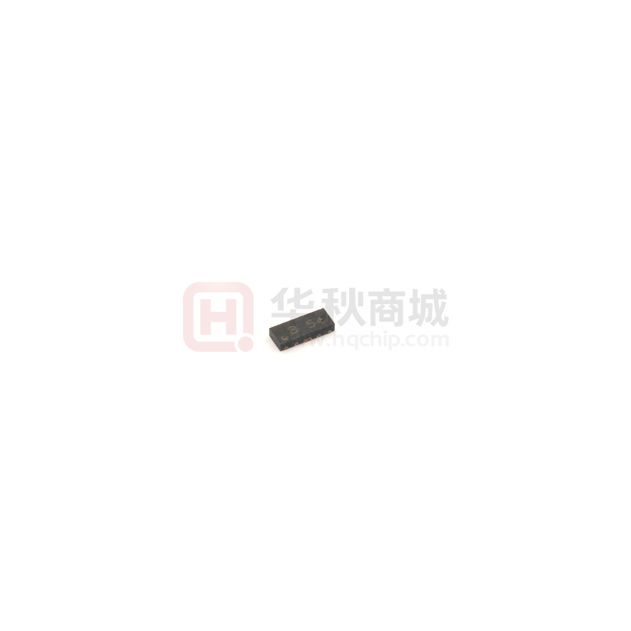
UBQ10A05L04HI
Electrostatic Discharged Protection Devices (ESD) Data Sheet
Description
UBQ10A05L04HI is a ultra low capacitance TVS array designed to
protect high speed data interfaces. This series has been specifically
designed to protect sensitive components which are connected to
high-speed data and transmission lines from over-voltage caused
by electrostatic discharge (ESD), cable discharge events (CDE),
and electrical fast transients (EFT). It has a typical capacitance of
only 0.3pF between I/O pins. This allows it to be used on circuits
operating in excess of 3GHz without signal attenuation. They may
be used to meet the ESD immunity requirements of IEC61000-4-2.
They are designed for easy PCB layout by allowing the traces to
run straight through the device. The combination of small size, low
capacitance, and high level of ESD protection makes them a flexible
solution for applications such as HDMI, UDI, Display PortTM, MDDI,
Serial ATA and Infiniband circuits.
Features
1
2
3
4
5
10
9
8
7
6
Pin Configuration
TMDS D2+
1
IEC61000-4-2 ESD 20kV Air, 20kV contact compliance
QFN-10 (2.5×1.0×0.5mm) surface mount package
Protects four I/O lines
Working voltage: 5V
Low leakage current
Low operating and clamping voltages
Solid-state silicon avalanche technology
Lead Free/RoHS compliant
Solder reflow temperature: Pure Tin-Sn, 260~270℃
Flammability rating UL 94V-0
Meets MSL level 1, per J-STD-020
Marking: B 54
10
●
●
●
●
●
●
●
●
●
●
●
●
TMDS D2-
TMDS D2-
GND
Applications
Revision:ESD-UBQ10A05L04HI -001(A1)
TMDS D1+
TMDS D1+
TMDS D1-
TMDS D1-
TMDS D0+
TMDS D0-
GND
1/5
1
High Definition Multimedia Interface (HDMI 1.4)
Digital Visual Interface (DVI)
Unified Display Interface (UDI)
Display Port Interface
MDDI Ports
PCI Express
Serial ATA
GND
10
●
●
●
●
●
●
●
TMDS D2+
TMDS D0+
TMDS D0-
GND
TMDS CK+
TMDS CK+
TMDS CK-
TMDS CK-
http://brightking.pulseelectronics.com
�UBQ10A05L04HI
Maximum Ratings
Rating
Symbol
Value
Unit
IPP
5
A
Peak Pulse Current (tp=8/20μs)
ESD voltage (Contact discharge)
±20
VESD
kV
ESD voltage (Air discharge)
±20
Storage & operating temperature range
TSTG ,TJ
℃
-55~+150
Electrical Characteristics (TJ=25℃)
Parameter
Reverse stand-off voltage
Reverse breakdown voltage
Symbol
Condition
Min.
Typ.
VRWM
Max.
Unit
5
V
VBR
IBR=1mA
Reverse leakage current
IR
VR=5V
Each I/O pin
1
μA
Clamping voltage (tp=8/20μs)
VC
IPP=1A
9.8
V
Clamping voltage (tp=8/20μs)
VC
IPP=4A
15
V
Off state junction capacitance
Revision:ESD-UBQ10A05L04HI -001(A1)
6
V
0Vdc,f=1MHz
I/O pin to GND
0.6
pF
0Vdc,f=1MHz
Between I/O pins
0.3
pF
CJ
2/5
http://brightking.pulseelectronics.com
�UBQ10A05L04HI
ESD Protection Standards
IEC61000-4-2
Interfaces of consumer electronic equipment are widely specified according to the International
Electrotechnical Commission standard IEC61000-4-2. This standard is not targeted towards
particular devices but towards general equipment, systems and subsystems that may be involved
in electrostatic discharge. consists of a 150pF capacitor and a 330Ω series resistor representing
the counterpart to the Device Under Test (DUT).
330Ω
50MΩ to 100MΩ
v
high-voltage
generator
150pF
DUT
001aaf202
Test circuit according IEC61000-4-2
IPP
100%
90%
10%
tr=0.7ns to 1ns
t
30ns
60ns
ESD surge according IEC61000-4-2
Revision:ESD-UBQ10A05L04HI -001(A1)
3/5
http://brightking.pulseelectronics.com
�UBQ10A05L04HI
Recommended Soldering Conditions
Reflow Soldering
Critical Zone
TL to TP
tP
TP
Ramp-up
TL
tL
Temperature
TS max
TS min
Ramp-down
tS
Preheat
25
t 25℃ to Peak
Time
Recommended Conditions
Profile Feature
Pb-Free Assembly
Average ramp-up rate (TL to TP)
3℃/second max.
Preheat
-Temperature Min (TS min)
-Temperature Max (TS max)
-Time (min to max) (ts)
150℃
200℃
60-180 seconds
TS max to TL
-Ramp-up Rate
3℃/second max.
Time maintained above:
-Temperature (TL)
-Time (tL)
217℃
60-150 seconds
Peak Temperature (TP)
260℃
Time within 5℃ of actual Peak Temperature (tP)
Ramp-down Rate
6℃/second max.
Time 25℃ to Peak Temperature
Revision:ESD-UBQ10A05L04HI -001(A1)
20-40 seconds
8 minutes max.
4/5
http://brightking.pulseelectronics.com
�UBQ10A05L04HI
Dimensions (QFN-10)
Dimension
D
Symbol
1
E
L
10
e
b2
b1
Millimeters
Inches
Min.
Nom.
Max.
Min.
Nom.
Max.
A
0.45
0.55
0.65
0.018
0.022
0.026
A1
-
0.03
0.05
-
0.001
0.002
A
A2
A2
A1
1.00
0.675
1.55
0.20
0.875
0.50
Recommended Soldering Pad Layout
0.005REF
b1
0.15
0.20
0.25
0.006
0.008
0.010
b2
0.35
0.40
0.45
0.014
0.016
0.018
D
2.40
2.50
2.60
0.094
0.098
0.102
E
0.90
1.00
1.10
0.035
0.039
0.043
e
0.20
0.40
0.13REF
L
0.50BSC
0.30
0.38
0.020BSC
0.43
0.012
0.015
0.017
Packaging
Tape
Pin Code
P0
P1
P2
K
F
B
W
E
øD0
A
øD1
t
Reel
D2
D
Revision:ESD-UBQ10A05L04HI -001(A1)
W1
5/5
Symbol
Dimension (mm)
W
8.00±0.30
P0
4.00±0.10
P1
4.00±0.10
P2
2.00±0.10
D0
Φ1.55±0.10
D1
Φ0.80±0.05
E
1.75±0.10
F
3.50±0.10
A
1.22±0.10
B
2.70±0.10
K
0.70±0.05
t
0.25±0.05
D
Φ178.0±2.0
D2
Φ13.0
W1
9.5
Quantity: 3000PCS
http://brightking.pulseelectronics.com
�
很抱歉,暂时无法提供与“UBQ10A05L04HI”相匹配的价格&库存,您可以联系我们找货
免费人工找货- 国内价格
- 1+0.39930
- 200+0.25740
- 1500+0.22330
- 3000+0.19800
- 国内价格
- 10+0.26649
- 50+0.24609
- 200+0.22909
- 600+0.21210
- 1500+0.19850
- 3000+0.19000
- 国内价格
- 10+0.39580
- 100+0.30810
- 300+0.26540
- 3000+0.23340
- 国内价格
- 20+1.06520
- 100+0.63550
- 800+0.44480
- 3000+0.31770
- 6000+0.30190
- 30000+0.27960
- 国内价格
- 10+0.39734
- 100+0.31148
- 300+0.26860
- 3000+0.23642
